

Page 1
www.fairchildsemi.com
RC4156/RC4157
High Performance Quad Operational Amplifiers
Features
• Unity gain bandwidth for RC4156 – 3.5 MHz
• Unity gain bandwidth for RC4157 – 19 MHz
• High slew rate for RC4156 – 1.6 V/µS
• High slew rate for RC4157 – 8.0V/µS
Description
The RC4156 and RC4157 are monolithic integrated circuits,
consisting of four independent high performance operational
amplifiers constructed with an advanced epitaxial process.
These amplifiers feature improved AC performance which
far exceeds that of the 741 type amplifiers. Also featured are
• Low noise voltage – 1.4 µVRMS
• Indefinite short circuit protection
• No crossover distortion
excellent input characteristics and low noise, making this
device the optimum choice for audio, active filter and instrumentation applications. The RC4157 is a decompensated
version of the RC4156 and is AC stable in gain configurations of -5 or greater.
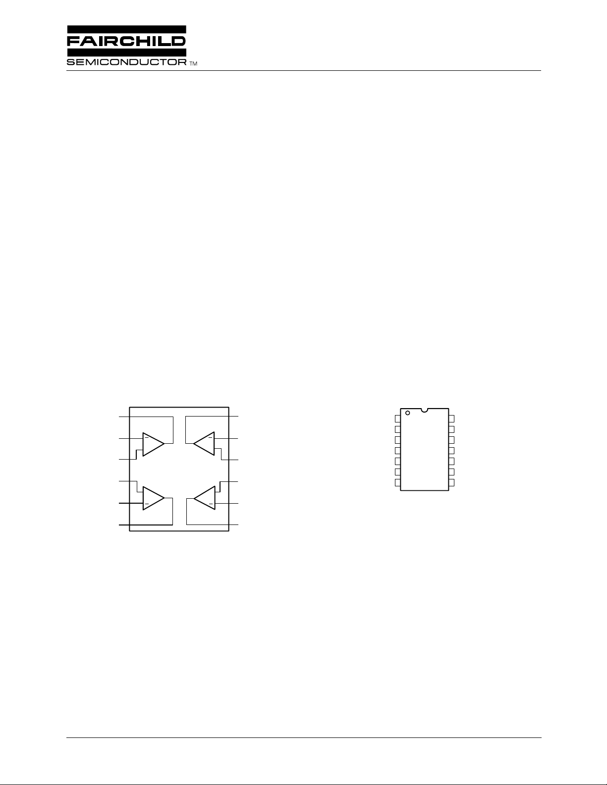
Block Diagram
Output (A)
–Input (A)
+Input (A)
+Input (B)
–Input (B)
Output (B)
A
+
+
B
D
+
+
C
65-3463-01
Output (D)
–Input (D)
+Input (D)
+Input (C)
–Input (C)
Output (C)
Pin Assignments
+V
1
2
3
4
S
5
6
7
Output (A)
–Input (A)
+Input (A)
+Input (B)
–Input (B)
Output (B)
14
13
12
11
10
65-3463-02
9
8
Output (D)
–Input (D)
+Input (D)
–V
S
+Input (C)
–Input (C)
Output (C)
REV. 1.0.1 6/13/01
Page 2
PRODUCT SPECIFICATION RC4156/RC4157
Absolute Maximum Ratings
(beyond which the device may be damaged)
Parameter Min Typ Max Units
Supply Voltage ±20 V
Input Voltage
Differential Input Voltage 30 V
Output Short Circuit Duration
< 50°C SOIC 300 mW
P
DTA
Operating Temperature RC4156/RC4157 0 70 °C
Storage Temperature -65 150 °C
Junction Temperature SOIC, PDIP 125 °C
Lead Soldering Temperature
(60 seconds)
For T
A
Notes:
1. Functional operation under any of these conditions is NOT implied. Performance and reliability are guaranteed only if
Operating Conditions are not exceeded.
2. For supply voltages less than ±15V, the absolute maximum input voltage is equal to the supply voltage.
3. Short circuit to ground on one amplifier only.
2
3
> 50°C Derate at SOIC 5.0 mW/°C
1
±15 V
Indefinite
PDIP 468 mW
DIP 300 °C
SOIC 260 °C
PDIP 6.25 mW/°C
Operating Conditions
Parameter Min Typ Max Units
θ
JC
θ
JA
Thermal resistance 60 °C/W
Thermal resistance SOIC 200 °C/W
PDIP 160 °C/W
Electrical Characteristics
(VS = ±15V, RC = 0°C ≤ TA ≤ +70°C)
RC4156/4157
Parameters Test Conditions Min Typ Max Units
Input Offset Voltage RS ≤ 10 kΩ 6.5 mV
Input Offset Current 100 nA
Input Bias Current 400 nA
Large Signal Voltage Gain RL ≥ 2 kΩ,V
Output Voltage Swing RL ≥ 2 kΩ ±10 V
Supply Current 10 mA
Average Input Offset Voltage Drift 5.0 µV/°C
±10V 15 V/mV
OUT
2 REV. 1.0.1 6/13/01
Page 3

RC4156/RC4157 PRODUCT SPECIFICATION
Electrical Characteristics
(VS = ±15V and TA = +25°C unless otherwise noted)
RC4156/4157
UnitsParameters Test Conditions Min Typ Max
Input Offset Voltage R
Input Offset Current 30 50 nA
Input Bias Current 60 300 nA
Input Resistance 0.5 MΩ
Large Signal Voltage Gain R
Output Voltage Swing R
Input Voltage Range ±12 ±14 V
Output Resistance 230 Ω
Short Circuit Current 25 mA
Common Mode Rejection Ratio RS ≤ 10 kΩ 80 dB
Power Supply Rejection Ratio RS ≤ 10 kΩ 80 dB
Supply Current (All Amplifiers) RL = ∞ 5.0 7.0 mA
Transient Response (4156)
Rise Time 60 nS
Overshoot 25 %
Slew Rate 1.3 1.6 V/µS
Unity Gain Bandwidth (4156) 2.8 3.5 MHz
Phase Margin (4156) RL = 2 kΩ, CL = 50 pF 50 %
Transient Response (4157) AV = -5
Rise Time 50 nS
Overshoot 25 %
Slew Rate 6.5 8.0 V/µS
Unity Gain Bandwidth (4157) AV = -5 15 19 MHz
Phase Margin (4157) AV = -5, RL = 2 kΩ,
Power Bandwidth V
Input Noise Voltage
1
Input Noise Current F = 20 Hz to 20 kHz 15 pA
Channel Separation 108 dB
Note:
1. Sample tested only.
≤ 10 kΩ 1.0 5.0 mV
S
≥ 2 kΩ, V
L
≥ 10 kΩ ±12 ±14 V
L
±10V 25 100 V/mV
OUT
RL ≥ 2 kΩ ±10 ±13 V
50 %
CL = 50 pF
OUT
= 20V
p-p
20 25 kHz
F = 20 Hz to 20 kHz 1.4 5.0 µV
RMS
RMS
REV. 1.0.1 6/13/01 3
Page 4
PRODUCT SPECIFICATION RC4156/RC4157
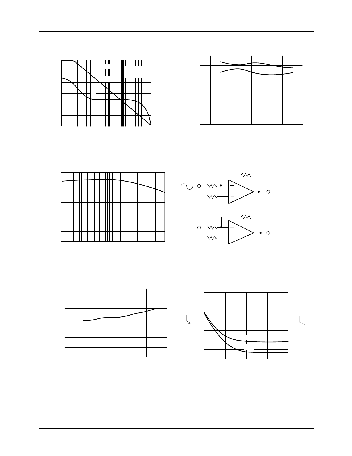
Typical Performance Characteristics
140
110
100
(dB)
VOL
A
-10
90
80
70
60
50
40
30
20
10
4156
A
VOL
R = 2K
L
C = 55 pF
L
0
45
Φ
90
Φ (Deg)
135
0
10
100
1K 10K 100K
1
1M
10M
180
65-0738
F (Hz)
120
100
80
60
PSRR (dB)
40
20
0
-100
-50
-V
S
0
TA (°C)
+V
S
65-0740
+50 +100 +150-25 +25 +75 +125-75
Figure 1. Open Loop Gain, Phase vs. Frequency Figure 2. PSRR vs. Temperature
2
3
6
5
100K
4156/57
100K
4156/57
1
7
V
OUT1
C.S. = 20 log ( )
V
100 V
OUT2
V
OUT2
65-0739
OUT1
-140
-120
1K
-100
-80
-60
CS (dB)
-40
1K
1K
-20
0
10 100 1K 10K 100K
1K
F (Hz)
Figure 3. Channel Separation vs. Frequency
1.3
35
1.2
1.1
1.0
0.9
0.8
Transient Response
(Normalized to +25°C)
0.7
0.6
-100 -50
65-0741
0 +50 +100 +150-75 -25 +25 +75 +125
TA (°C)
30
25
20
15
(nV Hz )
n
e
10
5
e
n
I
N
0
10 100 1K 10K 100K
F (Hz)
Figure 4. Transient Response vs. Temperature Figure 5. Input Noise Voltage, Current
Density vs. Frequency
1.4
1.2
1.0
0.8
0.6
0.4
0.2
0
(pA Hz )
N
I
65-0742
4 REV. 1.0.1 6/13/01
Page 5

RC4156/RC4157 PRODUCT SPECIFICATION
Typical Performance Characteristics (continued)
1.3
1.1
1.2
1.1
1.0
0.9
SR,BW
0.8
(Normalized to +25°C)
0.7
0.6
-100
-50 0 +50 +100
TA (°C)
65-0743
+150
1.0
0.9
SR, BW
0.8
(Normalized to ±15V)
0.7
SR and
BW
0
±2 ±5 ±10 ±15 ±20
±VS (V)
Figure 6. Slew Rate, Bandwidth vs. Temperature Figure 7. Slew Rate, Bandwidth vs. Supply Voltage
30
V
= 28V VS = ±15V
(V)
30
10
OUT P-P
V
OUT P-P
V
OUT P-P
= 18V VS = ±10V
= 8V VS = ±5V
25
20
(V)
15
OUT P-P
1.0
V
4156
(Voltage Follower)
R = Open
L
C = 50 pF
L
0.1
100 1K 10K
F (Hz)
100K
65-0746
1M
OUT P-P
V
100
10
05
0
1K
RL ( )
10K 100K
Ω
BW
65-0744
65-0749
Figure 8. Output Voltage Swing vs. Frequency Figure 9. Output Voltage Swing vs. Load Resistance
70
60
50
40
30
ΦM (Deg)
20
10
0
10 100
ΦM
BW
1K
4156
10K 100K
7
6
5
4
3
2
1
0
BW (MHz)
65-0745
CL (pF)
Figure 10. Small Signal Phase Margin,
Unity Gain Bandwidth vs. Load Capacitance
REV. 1.0.1 6/13/01 5
Page 6

PRODUCT SPECIFICATION RC4156/RC4157
Typical Performance Characteristics (continued)
140
120
100
80
(nA)
OS
60
, I
B
I
40
20
0-
-100 -75
Figure 11. Input Bias, Offset Current vs. Temperature Figure 12. CMRR vs. Temperature
-25 0 +25 +50 +75 +100
-50
TA (°C)
I
B
I
OS
Applications
The RC4156 and RC4157 quad operational amplifiers can be
used in almost any 741 application and will provide superior
performance. The higher unity gain bandwidth and slew rate
make it ideal for applications requiring good frequency
response, such as active filter circuits, oscillators and audio
amplifiers.
The following applications have been selected to illustrate
the advantages of using the Fairchild Semiconductor
RC4156 and RC4157 quad operational amplifiers.
Triangle and Square Wave Generator
The circuit of Figure 13 uses a positive feedback loop closed
around a combined comparator and integrator. When power
is applied the output of the comparator will switch to one of
two states, to the maximum positive or maximum negative
voltage. This applies a peak input signal to the integrator,
and the integrator output will ramp either down or up, opposite of the input signal. When the integrator output (which is
connected to the comparator input) reaches a threshold set by
R1 and R2, the comparator will switch to the opposite polarity. This cycle will repeat endlessly, the integrator charging
+125+150
140
120
100
80
60
CMRR (dB)
40
20
65-0747
0
-100 -75
-25 0 +25 +50 +75 +100
-50
TA (°C)
positive then negative, and the comparator switching in a
square wave fashion.
The amplitude of V
is adjusted by varying R1. For best
2
operation, it is recommended that R1 and VR be set to obtain
a triangle wave at V2 with ±12V amplitude. This will then
allow A3 and A4 to be used for independent adjustment of
output-offset and amplitude over a wide range.
The triangle wave frequency is set by C0, R0, and the maximum output voltages of the comparator. A more symmetrical
waveform can be generated by adding a back-to-back Zener
diode pair as shown in Figure 14.
An asymmetric triangle wave is needed in some applications.
Adding diodes as shown by the dashed lines is a way to vary
the positive and negative slopes independently.
The frequency range can be very wide and the circuit will
function well up to about 10 kHz. The square wave transition time at V
is less than 21 µS when using the RC4156.
1
65-0748
+125+150
6 REV. 1.0.1 6/13/01
Page 7

RC4156/RC4157 PRODUCT SPECIFICATION
+12V
20K
8
(+)
Amplitude
Adjust
V4
Triangle
Wave
Output
30K
1K
+15V
V 0.12V~
R
2
3
~
4156/57
A
20K
R1
R2
20K
1
5K
V1
Square Wave
Output
R0
100K
*
10K
6
4156/57
5
C0
B
-12V
R4
1K
V2
7
R3
20K
9
10
1K
+15V
4
4156/57
C
11
-15V
Comparator
* Optional – asymmetric ramp slopes
Integrator
+15V
-15V
Figure 13. Triangle and Square Wave Generator
R1
Figure 14. Triangle Generator—Symmetrical Output Option
Active Filters
The introduction of low-cost quad op amps has had a strong
impact on active filter design. The complex multiplefeedback, single op amp filter circuits have been rendered
obsolete for most applications. State-variable active-filter
circuits using three to four op amps per section offer many
advantages over the single op amp circuits. They are relatively insensitive to the passive-component tolerances and
variations. The Q, gain, and natural frequency can be independently adjusted. Hybrid construction is very practical
because resistor and capacitor values are relatively low and
the filter parameters are determined by resistance ratios
rather than by single resistors. A generalized circuit diagram
of the 2-pole state-variable active filter is shown in Figure
15. The particular input connections and component-values
can be calculated for specific applications. An important feature of the state-variable filter is that it can be inverting or
non-inverting and can simultaneously provide three outputs:
5K
5K
13
12
Output
Offset
4156/57
D
14
V3
65-0750
10K
65-2051
lowpass, bandpass, and highpass. A notch filter can be realized by adding one summing op amp.
The RC4156 was designed and characterized for use in
active filter circuits. Frequency response is fully specified
with minimum values for unity-gain bandwidth, slew-rate,
and full-power response. Maximum noise is specified.
Output swing is excellent with no distortion or clipping. The
RC4156 provides full, undistorted response up to 20 kHz
and is ideal for use in high-performance audio and telecommunication equipment.
In the state-variable filter circuit, one amplifier performs a
summing function and the other two act as integrators. The
choice of passive component values is arbitrary, but must be
consistent with the amplifier operating range and input signal
REV. 1.0.1 6/13/01 7
Page 8

PRODUCT SPECIFICATION RC4156/RC4157
Ts()
a
2
s2a1sa
0
++
s
2
b1sb
0
++
------------------------------------=
Q
ω
0
b
0
------=
R5
100K
R4
10K
V1
R3*
2
4156/57
R7*
3
R6
100K
R8*
V
N
* Input connections are chosen for inverting or non-inverting response. Values of
R3,R7,R8 determine gain and Q.
** Values of R1 and R2 determine natural frequency.
1
A
V
Highpass
Ouput
Figure 15. 2-Pole State-Variable Active Filter
characteristics. The values shown for C1, C2, R4, R5 and R6
are arbitrary. Pre-selecting their values will simplify the filter
tuning procedures, but other values can be used if necessary.
The generalized transfer function for the state-variable active
filter is:
9
10
C2
1000 pF
4156/57
C
8
V
LP
Lowpass
Output
65-0751
C1
1000 pF
7
V
BP
Bandpass
Output
R2**
R1**
HP
6
4156/57
5
B
The input configuration determines the polarity (inverting or
non-inverting), and the output selection determines the type
of filter response (lowpass, bandpass, or highpass).
Notch and all-pass configurations can be implemented by
adding another summing amplifier.
Filter response is conventionally described in terms of a natural frequency ω0 in radians/sec, and Q, the quality of the
complex pole pair. The filter parameters ω0 and Q relate to
the coefficients in T(s) as:
ω
0
and
b0=
R3R5
--------------------R3 R5+
----------------------------------R3R5
R4
---------------------+
R3 R5+
V
s()
HP
R3R4
--------------------R3 R4+
----------------------------------R3R4
R5
---------------------+
R3 R4+
V
LP
Equation 1.
Bandpass filters are of particular importance in audio and
telecommunication equipment. A design approach to bandpass filters will be shown as an example of the state-variable
configuration.
Design Example Bandpass Filter
For the bandpass active filter (Figure 16) the input signal is
applied through R3 to the inverting input of the summing
amplifier and the output is taken from the first integrator
(VBP). The summing amplifier will maintain equal voltage at
the inverting and non-inverting inputs (see Equation 1).
R4R5
--------------------R4 R5+
-----------------------------------
s()
R3
R4R5
---------------------+
R4 R5+
V
IN
s()
R7
--------------------R6 R7+
VBPs()+++
8 REV. 1.0.1 6/13/01
Page 9

RC4156/RC4157 PRODUCT SPECIFICATION
VBPs()
1
R1C1S
------------------
VHPs()–=
ω
0
0.1ω1ω
2
=
Q
1
10
5
R7
--------+
1.1
10
4
R3
--------+
----------------------
ω
0
=
Trim
Gain
and Q
R5
100K
R4
R3
V
IN
R7
10K
2
1
3
RC4156/57
A
Set Center Frequency
R6
100K
Figure 16. Bandpass Active Filter
These equations can be combined to obtain the transfer function:
1
-----------------R2C2S
1
---------------
S⋅
R1C1
1
---------------
S
R1C1
VBPs()–=
R4
-------
------------------------------
R5
R1C1R2C2
V
BP
-----------------V
IN
s()
s()
and
VLPs()
R4
-------
-------------------------------------------------------------------------------------------------------------------------------------------------------=
R7
2
---------------------
S
++
R6 R7+
1
R4
------R5
R3
R4
-------++
R3
1
6
5
RC4156/57
C1
1000 pF
7
B
C2
1000 pF
9
R2R1
10
V
BP
8
RC4156/57
C
65-0752
Defining 1/R1C1 as ω1, 1/R2C2 as ω2, and substituting in
the assigned values for R4, R5, and R6, then the transfer
function simplifies to:
4
10
--------
ω
s⋅
VBPs()
-----------------V
s()
IN
----------------------------------------------------------------------=
S
2
1.1
----------------------
1
R3
10
--------+
10
--------+
R7
R3
1
4
ω
5
1
s
-------------++
1
ω
1ω2
This is now in a convenient form to look at the centerfrequency ω0 and filter Q.
ω0109–0.1R1R2=
and
The frequency responses for various values of Q are shown
in Figure 17.
0
-10
-20
-30
(dB)
-40
-50
-60
0.1 1.0 10
Q = 0.5
Q = 1.0
Q = 2.0
Q = 5.0
Q = 10
Q = 20
Q = 50
Q = 100
65-0753
ω
ω
o
1
ω
ω
o
V
BP
=
V
IN
1 -
ω
ω
o
Figure 17. Bandpass Transfer Characteristics Normalized
for Unity Gain and Frequency
Q
2
2
1
+
Q
2
ω
ω
o
REV. 1.0.1 6/13/01 9
Page 10

PRODUCT SPECIFICATION RC4156/RC4157
These equations suggest a tuning sequence where ω is first
trimmed via R1 or R2, then Q is trimmed by varying R7
and/or R3. An important advantage of the state-variable
bandpass filter is that Q can be varied without affecting
center frequency ω
.
0
This analysis has assumed ideal op amps operating within
their linear range, which is a valid design approach for a
reasonable range of ω
and Q. At extremes of ω0 and at high
0
values of Q, the op amp parameters become significant. A
rigorous analysis is very complex, but some factors are particularly important in designing active filters.
1. The passive component values should be chosen such
that all op amps are operating within their linear region
for the anticipated range of input signals. Slew rate, output current rating, and common-mode input range must
be considered. For the integrators, the current through
the feedback capacitor (I = C dV/dt) should be included
in the output current computations.
Schematic Diagram (1/4 shown)
2. From the equation for Q, it should seem that infinite Q
could be obtained by making R7 zero. But as R7 is made
small, the Q becomes limited by the op amp gain at the
frequency of interest. The effective closed-loop gain is
being increased directly as R7 is made smaller, and the
ratio of open-loop gain to closed-loop gain is becoming
less. The gain and phase error of the filter at high Q is
very dependent on the op amp open-loop gain at w
.
0
3. The attenuation at extremes of frequency is limited by
the op amp gain and unity-gain bandwidth. For integrators, the finite open-loop op amp gain limits the accuracy at the low-end. The open-loop roll-off of gain limits
the filter attenuation at high frequency.
The RC4156 quad operational amplifier has much better frequency response than a conventional 741 circuit and is ideal
for active filter use. Natural frequencies of up to 10 kHz are
readily achieved and up to 20 kHz is practical for some configurations. Q can range up to 50 with very good accuracy
and up to 500 with reasonable response. The extra gain of the
RC4156 at high frequencies gives the quad op amp an extra
margin of performance in active-filter circuits.
(1,7,8,14)
Outputs
F1
(4)
+V
(11)
-V
s
s
R1
4900
(2,6,9,13)
- Input
+ Input
(3,5,10,12)
65-0735
Q8
Q4
Q2
R3
18K
Q7
Q5
Q9
Q10
Q3
R4
22K
D2
C1
R9
30
R5
30K
Q13
Q11
Q15
Q12
Q16
Q17
Q14
R6
20
R7
20
R8
150
Q1
Next
Amplifier
Q6
R2
10K
To
D1
10 REV. 1.0.1 6/13/01
Page 11

RC4156/RC4157 PRODUCT SPECIFICATION
Mechanical Dimensions (continued)
14-Lead Plastic DIP Package
Symbol
A — .210 — 5.33
A1 .015 — .38 —
A2 .115 2.93
B .014 .36
B1 .045 .070 1.14 1.78
C .008 .015 .20 .38
D .725 .795 18.42 20.19
D1 .005 — .13 —
E
E1
e
eB — .430 — 10.92
L
N
E1
Inches
Min. Max. Min. Max.
.195 4.95
.022 .56
.300 .325 7.62 8.26
.240 .280 6.10 7.11
.100 BSC 2.54 BSC
.115 .200 2.92 5.08
14 14 5
D
7
Millimeters
1
Notes
4
2
2
Notes:
1.
Dimensioning and tolerancing per ANSI Y14.5M-1982.
2.
"D" and "E1" do not include mold flashing. Mold flash or protrusions
shall not exceed .010 inch (0.25mm).
3.
Terminal numbers are shown for reference only.
4.
"C" dimension does not include solder finish thickness.
5.
Symbol "N" is the maximum number of terminals.
8
D1
e
A
A1
B1
14
E
C
L
B
eB
REV. 1.0.1 6/13/01 11
Page 12

PRODUCT SPECIFICATION RC4156/RC4157
Mechanical Dimensions (continued)
14-Lead SOIC Package
Symbol
A .053 .069 1.35 1.75
A1 .004 .010 0.10 0.25
B .013 0.33
C .008 .010 0.19 0.25
D .336 .345 8.54 8.76
E .150 .158 3.81 4.01
e
H
h
L .016 .050 0.40 1.27
N14 14
α
ccc .004 0.10——
14 8
Inches
Min. Max. Min. Max.
.020 0.51
.050 BSC 1.27 BSC
.228 .244 5.79 6.20
.010 .020 0.25 0.50
0° 8° 0° 8°
Millimeters
EH
17
Notes
5
2
2
3
6
Notes:
1.
Dimensioning and tolerancing per ANSI Y14.5M-1982.
2.
"D" and "E" do not include mold flash. Mold flash or protrusions
shall not exceed .010 inch (0.25mm).
3.
"L" is the length of terminal for soldering to a substrate.
4.
Terminal numbers are shown for reference only.
5.
"C" dimension does not include solder finish thickness.
6.
Symbol "N" is the maximum number of terminals.
D
A
e
A1
SEATING
B
PLANE
– C –
LEAD COPLANARITY
ccc C
α
h x 45°
C
L
12 REV. 1.0.1 6/13/01
Page 13

PRODUCT SPECIFICATION RC4156/RC4157
Ordering Information
Product Number Temperature Range Screening Package Package Marking
RC4156N 0° to 70°C Commercial 14 Pin Plastic DIP RC4156N
RC4157N 0° to 70°C Commercial 14 Pin Plastic DIP RC4157N
RC4156M 0° to 70°C Commercial 14 Pin Wide SOIC RC4156M
RC4157M 0° to 70°C Commercial 14 Pin Wide SOIC RC4157M
DISCLAIMER
FAIRCHILD SEMICONDUCTOR RESERVES THE RIGHT TO MAKE CHANGES WITHOUT FURTHER NOTICE TO
ANY PRODUCTS HEREIN TO IMPROVE RELIABILITY, FUNCTION OR DESIGN. FAIRCHILD DOES NOT ASSUME
ANY LIABILITY ARISING OUT OF THE APPLICATION OR USE OF ANY PRODUCT OR CIRCUIT DESCRIBED HEREIN;
NEITHER DOES IT CONVEY ANY LICENSE UNDER ITS PATENT RIGHTS, NOR THE RIGHTS OF OTHERS.
LIFE SUPPORT POLICY
FAIRCHILD’S PRODUCTS ARE NOT AUTHORIZED FOR USE AS CRITICAL COMPONENTS IN LIFE SUPPORT DEVICES
OR SYSTEMS WITHOUT THE EXPRESS WRITTEN APPROVAL OF THE PRESIDENT OF FAIRCHILD SEMICONDUCTOR
CORPORATION. As used herein:
1. Life support devices or systems are devices or systems
which, (a) are intended for surgical implant into the body,
or (b) support or sustain life, and (c) whose failure to
perform when properly used in accordance with
instructions for use provided in the labeling, can be
reasonably expected to result in a significant injury of the
user.
2. A critical component in any component of a life support
device or system whose failure to perform can be
reasonably expected to cause the failure of the life support
device or system, or to affect its safety or effectiveness.
www.fairchildsemi.com
6/13/01 0.0m 003
© 2001 Fairchild Semiconductor Corporation
Stock#DS30004841
 Loading...