

Datasheet PIC32MX534F064H, PIC32MX564F064H, PIC32MX564F128H, PIC32MX575F256H, PIC32MX575F512H Datasheet
...
PIC32MX5XX/6XX/7XX
Family Data Sheet
High-Performance, USB, CAN and Ethernet
32-bit Flash Microcontrollers
© 2009-2011 Microchip Technology Inc. DS61156G
Note the following details of the code protection feature on Microchip devices:
• Microchip products meet the specification contained in their particular Microchip Data Sheet.
• Microchip believes that its family of products is one of the most secure families of its kind on the market today, when used in the
intended manner and under normal conditions.
• There are dishonest and possibly illegal methods used to breach the code protection feature. All of these methods, to our
knowledge, require using the Microchip products in a manner outside the operating specifications contained in Microchip’s Data
Sheets. Most likely, the person doing so is engaged in theft of intellectual property.
• Microchip is willing to work with the customer who is concerned about the integrity of their code.
• Neither Microchip nor any other semiconductor manufacturer can guarantee the security of their code. Code protection does not
mean that we are guaranteeing the product as “unbreakable.”
Code protection is constantly evolving. We at Microchip are committed to continuously improving the code protection features of our
products. Attempts to break Microchip’s code protection feature may be a violation of the Digital Millennium Copyright Act. If such acts
allow unauthorized access to your software or other copyrighted work, you may have a right to sue for relief under that Act.
Information contained in this publication regarding device
applications and the like is provided only for your convenience
and may be superseded by updates. It is your responsibility to
ensure that your application meets with your specifications.
MICROCHIP MAKES NO REPRESENTATIONS OR
WARRANTIES OF ANY KIND WHETHER EXPRESS OR
IMPLIED, WRITTEN OR ORAL, STATUTORY OR
OTHERWISE, RELATED TO THE INFORMATION,
INCLUDING BUT NOT LIMITED TO ITS CONDITION,
QUALITY, PERFORMANCE, MERCHANTABILITY OR
FITNESS FOR PURPOSE. Microchip disclaims all liability
arising from this information and its use. Use of Microchip
devices in life support and/or safety applications is entirely at
the buyer’s risk, and the buyer agrees to defend, indemnify and
hold harmless Microchip from any and all damages, claims,
suits, or expenses resulting from such use. No licenses are
conveyed, implicitly or otherwise, under any Microchip
intellectual property rights.
Trademarks
The Microchip name and logo, the Microchip logo, dsPIC,
K
EELOQ, KEELOQ logo, MPLAB, PIC, PICmicro, PICSTART,
32
PIC
logo, rfPIC and UNI/O are registered trademarks of
Microchip Technology Incorporated in the U.S.A. and other
countries.
FilterLab, Hampshire, HI-TECH C, Linear Active Thermistor,
MXDEV, MXLAB, SEEVAL and The Embedded Control
Solutions Company are registered trademarks of Microchip
Technology Incorporated in the U.S.A.
Analog-for-the-Digital Age, Application Maestro, CodeGuard,
dsPICDEM, dsPICDEM.net, dsPICworks, dsSPEAK, ECAN,
ECONOMONITOR, FanSense, HI-TIDE, In-Circuit Serial
Programming, ICSP, Mindi, MiWi, MPASM, MPLAB Certified
logo, MPLIB, MPLINK, mTouch, Omniscient Code
Generation, PICC, PICC-18, PICDEM, PICDEM.net, PICkit,
PICtail, REAL ICE, rfLAB, Select Mode, Total Endurance,
TSHARC, UniWinDriver, WiperLock and ZENA are
trademarks of Microchip Technology Incorporated in the
U.S.A. and other countries.
SQTP is a service mark of Microchip Technology Incorporated
in the U.S.A.
All other trademarks mentioned herein are property of their
respective companies.
© 2009-2011, Microchip Technology Incorporated, Printed in
the U.S.A., All Rights Reserved.
Printed on recycled paper.
ISBN: 978-1-61341-150-6
Microchip received ISO/TS-16949:2002 certification for its worldwide
headquarters, design and wafer fabrication facilities in Chandler and
Tempe, Arizona; Gresham, Oregon and design centers in California
and India. The Company’s quality system processes and procedures
are for its PIC
devices, Serial EEPROMs, microperipherals, nonvolatile memory and
analog products. In addition, Microchip’s quality system for the design
and manufacture of development systems is ISO 9001:2000 certified.
®
MCUs and dsPIC® DSCs, KEELOQ
®
code hopping
DS61156G-page 2 © 2009-2011 Microchip Technology Inc.

PIC32MX5XX/6XX/7XX
High-Performance, USB, CAN and Ethernet
32-bit Flash Microcontrollers
High-Performance 32-bit RISC CPU:
•MIPS32® M4K® 32-bit core with 5-stage pipeline
• 80 MHz maximum frequency
• 1.56 DMIPS/MHz (Dhrystone 2.1) performance
at zero Wait state Flash access
• Single-cycle multiply and high-performance divide
unit
• MIPS16e
• Two sets of 32 core register files (32-bit) to reduce
interrupt latency
• Prefetch Cache module to speed execution from
Flash
®
mode for up to 40% smaller code size
Microcontroller Features:
• Operating voltage range of 2.3V to 3.6V
• 64K to 512K Flash memory (plus an
additional 12 KB of Boot Flash)
• 16K to 128K SRAM memory
• Pin-compatible with most PIC24/dsPIC
devices
• Multiple power management modes
• Multiple interrupt vectors with individually
programmable priority
• Fail-Safe Clock Monitor mode
• Configurable Watchdog Timer with on-chip
Low-Power RC oscillator for reliable operation
®
DSC
Peripheral Features:
• Atomic SET, CLEAR and INVERT operation on
select peripheral registers
• Up to 8-channels of hardware DMA with automatic
data size detection
• USB 2.0-compliant full-speed device and
On-The-Go (OTG) controller:
- Dedicated DMA channels
• 10/100 Mbps Ethernet MAC with MII and RMII
interface:
- Dedicated DMA channels
• CAN module:
- 2.0B Active with DeviceNet™ addressing
support
- Dedicated DMA channels
• 3 MHz to 25 MHz crystal oscillator
Peripheral Features (Continued):
• Internal 8 MHz and 32 kHz oscillators
• Six UART modules with:
- RS-232, RS-485 and LIN support
-IrDA
• Up to four SPI modules
• Up to five I
• Separate PLLs for CPU and USB clocks
• Parallel Master and Slave Port (PMP/PSP) with
8-bit and 16-bit data, and up to 16 address lines
• Hardware Real-Time Clock and Calendar (RTCC)
• Five 16-bit Timers/Counters (two 16-bit pairs
combine to create two 32-bit timers)
• Five Capture inputs
• Five Compare/PWM outputs
• Five external interrupt pins
• High-speed I/O pins capable of toggling at up
to 80 MHz
• High-current sink/source (18 mA/18 mA) on
all I/O pins
• Configurable open-drain output on digital I/O pins
®
with on-chip hardware encoder and
decoder
2
C™ modules
Debug Features:
• Two programming and debugging Interfaces:
- 2-wire interface with unintrusive access and
real-time data exchange with application
- 4-wire MIPS
Action Group (JTAG) interface
• Unintrusive hardware-based instruction trace
• IEEE Standard 1149.2 compatible (JTAG)
boundary scan
®
standard enhanced Joint Test
Analog Features:
• Up to 16-channel, 10-bit Analog-to-Digital
Converter:
- 1 Msps conversion rate
- Conversion available during Sleep and Idle
• Two Analog Comparators
© 2009-2011 Microchip Technology Inc. DS61156G-page 3

PIC32MX5XX/6XX/7XX
TABLE 1: PIC32 USB AND CAN – FEATURES
USB and CAN
(3)
SPI
(3)
2
C™
I
(Channels)
Comparators
10-bit 1 Msps ADC
Device
Pins
Program Memory (KB)
PIC32MX534F064H 64 64 + 12
PIC32MX564F064H 64 64 + 12
PIC32MX564F128H 64 128 + 12
PIC32MX575F256H 64 256 + 12
PIC32MX575F512H 64 512 + 12
PIC32MX534F064L 100 64 + 12
PIC32MX564F064L 100 64 + 12
PIC32MX564F128L 100 128 + 12
PIC32MX575F256L 100 256 + 12
PIC32MX575F512L 100 512 + 12
(2,3)
USB
Data Memory (KB)
CAN
DMA Channels
UART
Dedicated)
(Programmable/
Timers/Capture/Compare
(1)
16 1 1 5/5/5 4/4 6 3 4 16 2 Yes Yes No
(1)
32 1 1 5/5/5 4/4 6 3 4 16 2 Yes Yes No
(1)
32 1 1 5/5/5 4/4 6 3 4 16 2 Yes Yes No
(1)
64 1 1 5/5/5 8/4 6 3 4 16 2 Yes Yes No
(1)
64 1 1 5/5/5 8/4 6 3 4 16 2 Yes Yes No
(1)
16 1 1 5/5/5 4/4 6 4 5 16 2 Yes Yes Yes
(1)
32 1 1 5/5/5 4/4 6 4 5 16 2 Yes Yes Yes
(1)
32 1 1 5/5/5 4/4 6 4 5 16 2 Yes Yes Yes
(1)
64 1 1 5/5/5 8/4 6 4 5 16 2 Yes Yes Yes
(1)
64 1 1 5/5/5 8/4 6 4 5 16 2 Yes Yes Yes
Legend: PF, PT = TQFP MR = QFN BG = XBGA
Note 1: This device features 12 KB boot Flash memory.
2: CTS and RTS pins may not be available for all UART modules. Refer to the “Pin Diagrams” section for more
information.
3: Some pins between the UART, SPI and I
2
C modules may be shared. Refer to the “Pin Diagrams” section for more
information.
4: Refer to Section 32.0 “Packaging Information” for more information.
PMP/PSP
JTAG
(4)
Trace
Packages
PT,
MR
PT,
MR
PT,
MR
PT,
MR
PT,
MR
PT,
PF,
BG
PT,
PF,
BG
PT,
PF,
BG
PT,
PF,
BG
PT,
PF,
BG
DS61156G-page 4 © 2009-2011 Microchip Technology Inc.

TABLE 2: PIC32 USB AND ETHERNET – FEATURES
USB and Ethernet
PIC32MX5XX/6XX/7XX
(3)
SPI
(3)
2
C™
I
(Channels)
10-bit 1 Msps ADC
Comparators
Device
Pins
Program Memory (KB)
PIC32MX664F064H 64 64 + 12
PIC32MX664F128H 64 128 + 12
PIC32MX675F256H 64 256 + 12
PIC32MX675F512H 64 512 + 12
PIC32MX695F512H 64 512 + 12
PIC32MX664F064L 100 64 + 12
PIC32MX664F128L 100 128 + 12
PIC32MX675F256L 100 256 + 12
PIC32MX675F512L 100 512 + 12
PIC32MX695F512L 100
512 + 12
(2,3)
USB
Ethernet
Data Memory (KB)
DMA Channels
UART
Dedicated)
(Programmable/
Timers/Capture/Compare
(1)
32 1 1 5/5/5 4/4 6 3 4 16 2 Yes Yes No
(1)
32 1 1 5/5/5 4/4 6 3 4 16 2 Yes Yes No
(1)
64 1 1 5/5/5 8/4 6 3 4 16 2 Yes Yes No
(1)
64 1 1 5/5/5 8/4 6 3 4 16 2 Yes Yes No
(1)
128 1 1 5/5/5 8/4 6 3 4 16 2 Yes Yes No
(1)
32 1 1 5/5/5 4/4 6 4 5 16 2 Yes Yes Yes
(1)
32 1 1 5/5/5 4/4 6 4 5 16 2 Yes Yes Yes
(1)
64 1 1 5/5/5 8/4 6 4 5 16 2 Yes Yes Yes
(1)
64 1 1 5/5/5 8/4 6 4 5 16 2 Yes Yes Yes
(1)
128 1 1 5/5/5 8/4 6 4 5 16 2 Yes Yes Yes
Legend: PF, PT = TQFP MR = QFN BG = XBGA
Note 1: This device features 12 KB boot Flash memory.
2: CTS and RTS pins may not be available for all UART modules. Refer to the “Pin Diagrams” section for more
information.
3: Some pins between the UART, SPI and I
2
C modules may be shared. Refer to the “Pin Diagrams” section for more
information.
4: Refer to Section 32.0 “Packaging Information” for more information.
JTAG
PMP/PSP
(4)
Trace
Packages
PT,
MR
PT,
MR
PT,
MR
PT,
MR
PT,
MR
PT,
PF,
BG
PT,
PF,
BG
PT,
PF,
BG
PT,
PF,
BG
PT,
PF,
BG
© 2009-2011 Microchip Technology Inc. DS61156G-page 5

PIC32MX5XX/6XX/7XX
TABLE 3: PIC32 USB, ETHERNET AND CAN – FEATURES
USB, Ethernet and CAN
(3)
SPI
(3)
2
C™
I
(Channels)
Comparators
10-bit 1 Msps ADC
Device
Pins
Program Memory (KB)
PIC32MX764F128H 64 128 + 12
PIC32MX775F256H 64 256 + 12
PIC32MX775F512H 64 512 + 12
PIC32MX795F512H 64 512 + 12
PIC32MX764F128L 100 128 + 12
PIC32MX775F256L 100 256 + 12
PIC32MX775F512L 100 512 + 12
PIC32MX795F512L 100 512 + 12
(2,3)
USB
Data Memory (KB)
CAN
Ethernet
DMA Channels
UART
Dedicated)
(Programmable/
Timers/Capture/Compare
(1)
32 1 1 1 5/5/5 4/6 6 3 4 16 2 Yes Yes No
(1)
64 1 1 2 5/5/5 8/8 6 3 4 16 2 Yes Yes No
(1)
64 1 1 2 5/5/5 8/8 6 3 4 16 2 Yes Yes No
(1)
128 1 1 2 5/5/5 8/8 6 3 4 16 2 Yes Yes No
(1)
32 1 1 1 5/5/5 4/6 6 4 5 16 2 Yes Yes Yes
(1)
64 1 1 2 5/5/5 8/8 6 4 5 16 2 Yes Yes Yes
(1)
64 1 1 2 5/5/5 8/8 6 4 5 16 2 Yes Yes Yes
(1)
128 1 1 2 5/5/5 8/8 6 4 5 16 2 Yes Yes Yes
Legend: PF, PT = TQFP MR = QFN BG = XBGA
Note 1: This device features 12 KB boot Flash memory.
2: CTS and RTS pins may not be available for all UART modules. Refer to the “Pin Diagrams” section for more
information.
3: Some pins between the UART, SPI and I
2
C modules may be shared. Refer to the “Pin Diagrams” section for more
information.
4: Refer to Section 32.0 “Packaging Information” for more information.
PMP/PSP
JTAG
(4)
Trace
Packages
PT,
MR
PT,
MR
PT,
MR
PT,
MR
PT,
PF,
BG
PT,
PF,
BG
PT,
PF,
BG
PT,
PF,
BG
DS61156G-page 6 © 2009-2011 Microchip Technology Inc.
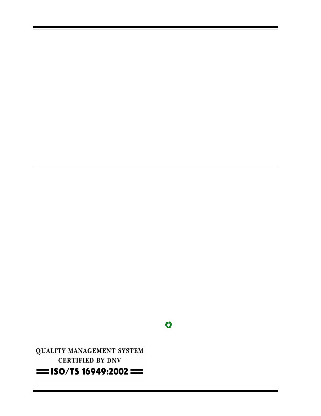
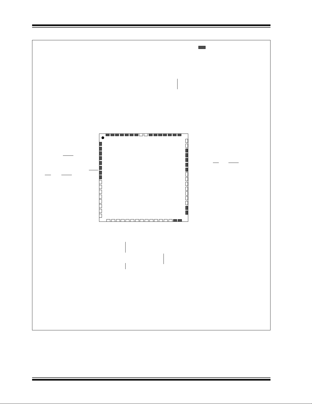
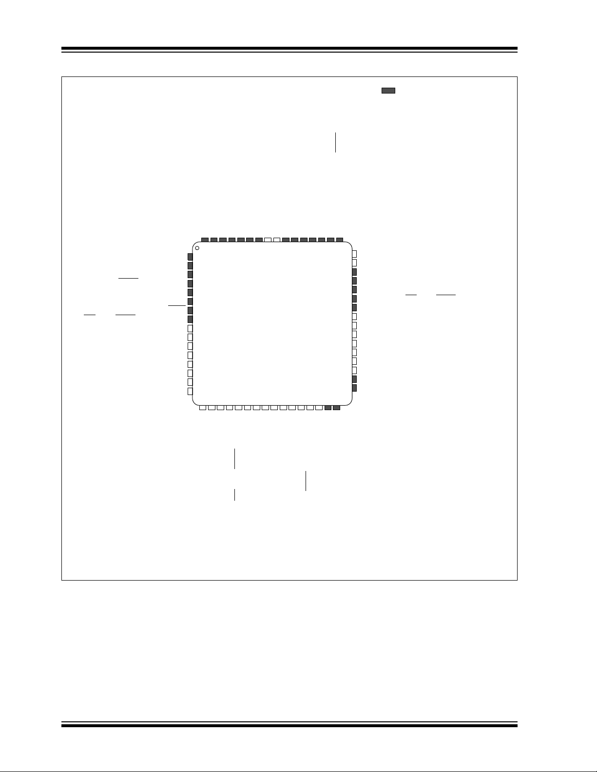
Pin Diagrams
64-Pin QFN
(1)
= Pins are up to 5V tolerant
Note 1: The metal plane at the bottom of the device is not connected to any pins and is recommended to be
connected to V
SS externally.
PIC32MX575F256H
PMD5/RE5
PMD6/RE6
PMD7/RE7
SCK2/U6TX/U3RTS
/PMA5/CN8/RG6
V
DD
AN5/C1IN+/VBUSON/CN7/RB5
AN4/C1IN-/CN6/RB4
AN3/C2IN+/CN5/RB3
AN2/C2IN-/CN4/RB2
SDA4/SDI2/U3RX/PMA4/CN9/RG7
SCL4/SDO2/U3TX/PMA3/CN10/RG8
PGEC1/AN1/V
REF-/CVREF-/CN3/RB1
PGED1/AN0/V
REF+/CVREF+/PMA6/CN2/RB0
SS2
/U6RX/U3CTS/PMA2/CN11/RG9
MCLR
VSS
64 63 62 61 60 59 58 57 56 55
22 23 24 25 26 27 28 29 30 31
3
40
39
38
37
36
35
34
33
4
5
7
8
9
10
11
1
2
42
41
6
32
43
54
14
15
16
12
13
17
18 19 20 21
45
44
47
46
48
53
52 51 50 49
AVDD
AN8/SS4/U5RX/U2CTS/C1OUT/RB8
AN9/C2OUT/PMA7/RB9
TMS/AN10/CV
REFOUT/PMA13/RB10
TDO/AN11/PMA12/RB11
V
DD
PGEC2/AN6/OCFA/RB6
PGED2/AN7/RB7
AC1RX/SCL5/SDO4/U2TX/PMA8/CN18/RF5
AC1TX/SDA5/SDI4/U2RX/PMA9/CN17/RF4
TCK/AN12/PMA11/RB12
TDI/AN13/PMA10/RB13
AN14/SCK4/U5TX/U2RTS
/PMALH/PMA1/RB14
AN15/OCFB/PMALL/PMA0/CN12/RB15
V
SS
AVSS
CN15/RD6
PMRD/CN14/RD5
OC5/IC5/PMWR/CN13/RD4
SCL3/SDO3/U1TX/OC4/RD3
SDA3/SDI3/U1RX/OC3/RD2
SCK3/U4TX/U1RTS
/OC2/RD1
PMD4/RE4
PMD3/RE3
PMD2/RE2
PMD1/RE1
C1RX/RF0
V
CAP/VCORE
PMD0/RE0
C1TX/RF1
CN16/RD7
V
DD
SOSCI/CN1/RC13
OC1/INT0/RD0
SCL1/IC3/PMCS2/PMA15/INT3/RD10
SS3
/U4RX/U1CTS/SDA1/IC2/INT2/RD9
RTCC/IC1/INT1/RD8
IC4/PMCS1/PMA14/INT4/RD11
OSC2/CLKO/RC15
OSC1/CLKI/RC12
V
DD
D+/RG2
V
USB
VBUS
USBID/RF3
D-/RG3
SOSCO/T1CK/CN0/RC14
Vss
PIC32MX575F512H
PIC32MX534F064H
PIC32MX564F064H
PIC32MX564F128H
PIC32MX5XX/6XX/7XX
© 2009-2011 Microchip Technology Inc. DS61156G-page 7
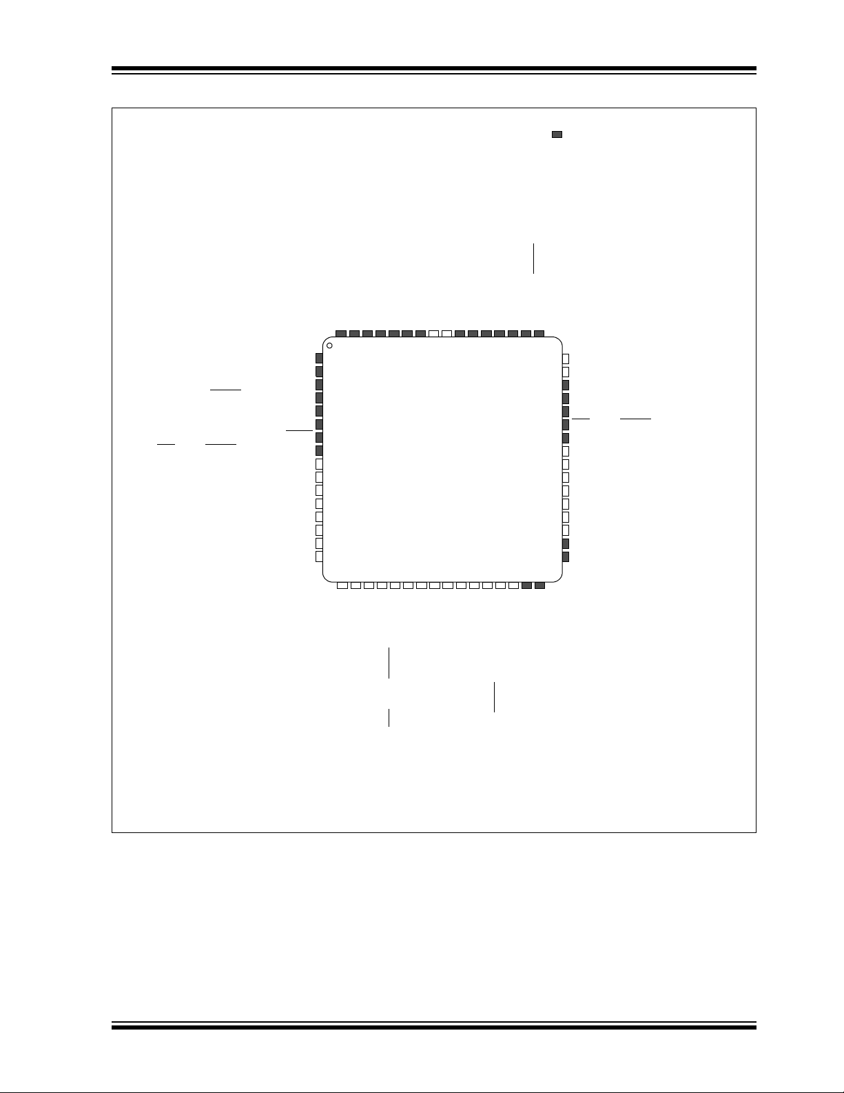
PIC32MX5XX/6XX/7XX
64-Pin QFN
(1)
= Pins are up to 5V tolerant
PIC32MX675F512H
PIC32MX695F512H
PIC32MX675F256H
22 23 24 25 26 27 28 29 30 31
40
39
38
37
36
35
34
33
42
41
32
43
17
18 19 20 21
45
44
47
46
48
AV
DD
AN8/SS4/U5RX/U2CTS/C1OUT/RB8
AN9/C2OUT/PMA7/RB9
TMS/AN10/CV
REFOUT
/PMA13/RB10
TDO/AN11/PMA12/RB11
V
DD
PGEC2/AN6/OCFA/RB6
PGED2/AN7/RB7
SCL5/SDO4/U2TX/PMA8/CN18/RF5
SDA5/SDI4/U2RX/PMA9/CN17/RF4
TCK/AN12/PMA11/RB12
TDI/AN13/PMA10/ RB13
AN14/SCK4/U5TX/U2RTSU2RTS
/PMALH/PMA1/RB14
AN15/EMDC/AEMDC/OCFB/PMALL/PMA0/CN12/RB15
V
SS
AV
SS
SOSCI/CN1/RC13
OC1/INT0/RD0
ECOL/AECRSDV/SCL1/IC3/PMCS2/PMA15/INT3/RD10
AERXD0/ETXD2/SS3
/U4RX/U1CTS/SDA1/IC2/INT2/RD9
RTCC/AERXD1/ETXD3/IC1/INT1/RD8
ECRS/AEREFCLK/IC4/PMCS1/PMA14/INT4/RD11
OSC2/CLKO/RC15
OSC1/CLKI/RC12
V
DD
D+/RG2
V
USB
V
BUS
USBID/RF3
D-/RG3
SOSCO/T1CK/CN0/RC14
Vss
ETXEN/PMD5/RE5
ETXD0/PMD6/RE6
ETXD1/PMD7/RE7
SCK2/U6TX/U3RTS
/PMA5/CN8/RG6
V
DD
AN5/C1IN+/V
BUSON
/CN7/RB5
AN4/C1IN-/CN6/RB4
AN3/C2IN+/CN5/ RB3
AN2/C2IN-/CN4/RB2
SDA4/SDI2/U3RX/PMA4/CN9/RG7
SCL4/SDO2/U3TX/PMA3/CN10/RG8
PGEC1/AN1/V
REF
-/CV
REF
-/CN3/RB1
PGED1/AN0/V
REF
+/CV
REF
+/PMA6/CN2/RB0
SS2
/U6RX/U3CTS/PMA2/CN11/RG9
MCLR
V
SS
64 63 62 61 60 59 58 57 56 55
3
4
5
7
8
9
10
11
1
2
6
54
14
15
16
12
13
53
52 51 50 49
AETXEN/ETXERR/CN15/RD6
PMRD/CN14/RD5
OC5/IC5/PMWR/CN13/RD4
SCL3/SDO3/U1TX/OC4/RD3
SDA3/SDI3/U1RX/OC3/RD2
EMDIO/AEMDIO/SCK3/U4TX/U1RTS
/OC2/RD1
ERXERR/PMD4/RE4
ERXCLK/EREFCLK/PMD3/RE3
ERXDV/ECRSDV/PMD2/RE2
ERXD0/PMD1/RE1
AETXD1/ERXD3/RF0
V
CAP
/V
CORE
ERXD1/PMD0/RE0
AETXD0/ERXD2/RF1
ETXCLK/AERXERR/CN16/RD7
V
DD
Note 1: The metal plane at the bottom of the device is not connected to any pins and is recommended to be
connected to VSS externally.
PIC32MX664F064H
PIC32MX664F128H
Pin Diagrams (Continued)
DS61156G-page 8 © 2009-2011 Microchip Technology Inc.
Pin Diagrams (Continued)
64-Pin QFN
(1)
= Pins are up to 5V tolerant
ETXEN/PMD5/RE5
ETXD0/PMD6/RE6
ETXD1/PMD7/RE7
SCK2/U6TX/U3RTS/PMA5/CN8/RG6
V
DD
AN5/C1IN+/V
BUSON
/CN7/RB5
AN4/C1IN-/CN6/RB4
AN3/C2IN+/CN5/ RB3
AN2/C2IN-/CN4/RB2
SDA4/SDI2/U3RX/PMA4/CN9/RG7
SCL4/SDO2/U3TX/PMA3/CN10/RG8
PGEC1/AN1/V
REF
-/CV
REF
-/CN3/RB1
PGED1/AN0/V
REF
+/CV
REF
+/PMA6/CN2/RB0
SS2
/U6RX/U3CTS/PMA2/CN11/RG9
MCLR
V
SS
64 63 62 61 60 59 58 57 56 55
3
4
5
7
8
9
10
11
1
2
6
54
14
15
16
12
13
53
52 51 50 49
AETXEN/ETXERR/CN15/RD6
PMRD/CN14/RD5
OC5/IC5/PMWR/CN13/RD4
SCL3/SDO3/U1TX/OC4/RD3
SDA3/SDI3/U1RX/ OC3/RD2
EMDIO/AEMDIO/SCK3/U4TX/U1RTS
/OC2/RD1
ERXERR/PMD4/RE4
ERXCLK/EREFCLKPMD3/RE3
ERXDV/ECRSDV/PMD2/RE2
ERXD0/PMD1/RE1
C1RX/AETXD1/ERXD3/RF0
V
CAP
/V
CORE
ERXD1/PMD0/RE0
C1TX/AETXD0/ERXD2/RF1
ETXCLK/AERXERR/CN16/RD7
V
DD
PIC32MX795F512H
PIC32MX775F256H
PIC32MX775F512H
22 23 24 25 26 27 28 29 30 31
40
39
38
37
36
35
34
33
42
41
32
43
17
18 19 20 21
45
44
47
46
48
AV
DD
AN8/C2TX/SS4/U5RX/U2CTS/C1OUT/RB8
AN9/C2OUT/PMA7/RB9
TMS/AN10/CV
REFOUT
/PMA13/RB10
TD O/A N11 /PM A12 /R B11
V
DD
PGEC2/AN6/OCFA/RB6
PGED2/AN7/RB7
AC1RX/SCL5/SDO4/U2TX/PMA8/CN18/RF5
AC1TX/SDA5/SDI4/U2RX/PMA9/CN17/RF4
TCK/AN12/PMA11/RB12
TDI/AN13/PMA10/RB13
AN14/C2RX/SCK4/U5TX/U2RTS
/PMALH/PMA1/RB14
AN15/EMDC/AEMDC/OCFB/PMALL/PMA0/CN12/RB15
V
SS
AV
SS
SOSCI/CN1/RC13
OC1/INT0/RD0
ECOL/AECRSDV/SCL1/IC3/PMCS2/PMA15/INT3/RD10
AERXD0/ETXD2/SS3
/U4RX/U1CTS/SDA1/IC2/INT2/RD9
RTCC/AERXD1/ETXD3/I C1/INT1/RD8
ECRS/AEREFCLK/IC4/PMCS1/PMA14/INT4/RD11
OSC2/CLKO/RC15
OSC1/CLKI/RC12
V
DD
D+/RG2
V
USB
V
BUS
USBID/RF3
D-/RG3
SOSCO/T1CK/CN0/RC14
Vss
Note 1: The metal plane at the bottom of the device is not connected to any pins and is recommended to be
connected to V
SS externally.
PIC32MX5XX/6XX/7XX
© 2009-2011 Microchip Technology Inc. DS61156G-page 9
PIC32MX5XX/6XX/7XX
64-Pin QFN
(1)
= Pins are up to 5V tolerant
ETXEN/PMD5/RE5
ETXD0/PMD6/RE6
ETXD1/PMD7/RE7
SCK2/U6TX/U3RTS/PMA5/CN8/RG6
V
DD
AN5/C1IN+/V
BUSON
/CN7/RB5
AN4/C1IN-/CN6/RB4
AN3/C2IN+/CN5/ RB3
AN2/C2IN-/CN4/RB2
SDA4/SDI2/U3RX/PMA4/CN9/RG7
SCL4/SDO2/U3TX/PMA3/CN10/RG8
PGEC1/AN1/V
REF
-/CV
REF
-/CN3/RB1
PGED1/AN0/V
REF
+/CV
REF
+/PMA6/CN2/RB0
SS2
/U6RX/U3CTS/PMA2/CN11/RG9
MCLR
V
SS
64 63 62 61 60 59 58 57 56 55
3
4
5
7
8
9
10
11
1
2
6
54
14
15
16
12
13
53
52 51 50 49
AETXEN/ETXERR/CN15/RD6
PMRD/CN14/RD5
OC5/IC5/PMWR/CN13/RD4
SCL3/SDO3/U1TX/OC4/RD3
SDA3/SDI3/U1RX/OC3/RD2
EMDIO/AEMDIO/SCK3/U4TX/U1RTS
/OC2/RD1
ERXERR/PMD4/RE4
ERXCLK/EREFCLKPMD3/RE3
ERXDV/ECRSDV/PMD2/RE2
ERXD0/PMD1/RE1
C1RX/AETXD1/ERXD3/RF0
V
CAP
/V
CORE
ERXD1/PMD0/RE0
C1TX/AETXD0/ERXD2/RF1
ETXCLK/AERXERR/CN16/RD7
V
DD
PIC32MX764F128H
22 23 24 25 26 27 28 29 30 31
40
39
38
37
36
35
34
33
42
41
32
43
17
18 19 20 21
45
44
47
46
48
AV
DD
AN8/SS4/U5RX/U2CTS/C1OUT/RB8
AN9/C2OUT/PMA7/RB9
TMS/AN10/CV
REFOUT
/PMA13/RB10
TDO/AN11/PMA12/RB11
V
DD
PGEC2/AN6/OCFA/RB6
PGED2/AN7/RB7
AC1RX/SCL5/SDO4/U2TX/PMA8/CN18/RF5
AC1TX/SDA5/SDI4/U2RX/PMA9/CN17/RF4
TCK/AN12/PMA11/RB12
TDI/AN13/PMA10/RB13
AN14/SCK4/U5TX/U2RTS
/PMALH/PMA1/RB14
AN15/EMDC/AEMDC/OCFB/PMALL/PMA0/CN12/RB15
V
SS
AV
SS
SOSCI/CN1/RC13
OC1/INT0/RD0
ECOL/AECRSDV/SCL1/IC3/PMCS2/PMA15/INT3/RD10
AERXD0/ETXD2/SS3
/U4RX/U1CTS/SDA1/IC2/INT2/RD9
RTCC/AERXD1/ETXD3/IC1/INT1/RD8
ECRS/AEREFCLK/IC4/PMCS1/PMA14/INT4/RD11
OSC2/CLKO/RC15
OSC1/CLKI/RC12
V
DD
D+/RG2
V
USB
V
BUS
USBID/RF3
D-/RG3
SOSCO/T1CK/CN0/RC14
Vss
Note 1: The metal plane at the bottom of the device is not connected to any pins and is recommended to be
connected to VSS externally.
Pin Diagrams (Continued)
DS61156G-page 10 © 2009-2011 Microchip Technology Inc.
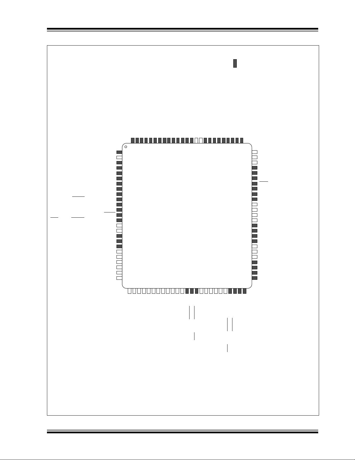
Pin Diagrams (Continued)
64-Pin TQFP
= Pins are up to 5V tolerant
PIC32MX575F256H
PMD5/RE5
PMD6/RE6
PMD7/RE7
SCK2/U6TX/U3RTS
/PMA5/CN8/RG6
V
DD
AN5/C1IN+/V
BUSON
/CN7/RB5
AN4/C1IN-/CN6/RB4
AN3/C2IN+/CN5/RB3
AN2/C2IN-/CN4/RB2
SDA4/SDI2/U3RX/PMA4/CN9/RG7
SCL4/SDO2/U3TX/PMA3/CN10/RG8
PGEC1/AN1/V
REF
-/CV
REF
-/CN3/RB1
PGED1/AN0/V
REF
+/CV
REF
+/PMA6/CN2/RB0
SS2
/U6RX/U3CTS/PMA2/CN11/RG9
MCLR
V
SS
64 63 62 61 60 59 58 57 56 55
22 23 24 25 26 27 28 29 30 31
3
40
39
38
37
36
35
34
33
4
5
7
8
9
10
11
1
2
42
41
6
32
43
54
14
15
16
12
13
17
18 19 20 21
45
44
47
46
48
53
52 51 50 49
AV
DD
AN8/SS4/U5RX/U2CTS/C1OUT/RB8
AN9/C2OUT/PMA7/RB9
TMS/AN10/CV
REFOUT
/PMA13/RB10
TDO/AN11/PMA12/RB11
V
DD
PGEC2/AN6/OCFA/RB6
PGED2/AN7/RB7
AC1RX/SCL5/SDO4/U2TX/PMA8/CN18/RF5
AC1TX/SDA5/SDI4/U2RX/PMA9/CN17/RF4
TCK/AN12/PMA11/RB12
TDI/AN13/PMA10/RB13
AN14/SCK4/U5TX/U2RTS
/PMALH/PMA1/RB14
AN15/OCFB/PMALL/PMA0/CN12/RB15
V
SS
AV
SS
CN15/RD6
PMRD/CN14/RD5
OC5/IC5/PMWR/CN13/RD4
SCL3/SDO3/U1TX/OC4/RD3
SDA3/SDI3/U1RX/OC3/RD2
SCK3/U4TX/U1RTS
/OC2/RD1
PMD4/RE4
PMD3/RE3
PMD2/RE2
PMD1/RE1
C1RX/RF0
V
CAP
/V
CORE
PMD0/RE0
C1TX/RF1
CN16/RD7
V
DD
SOSCI/CN1/RC13
OC1/INT0/RD0
SCL1/IC3/PMCS2/PMA15/INT3/RD10
SS3
/U4RX/U1CTS/SDA1/IC2/INT2/RD9
RTCC/IC1/INT1/RD8
IC4/PMCS1/PMA14/INT4/RD11
OSC2/CLKO/RC15
OSC1/CLKI/RC12
V
DD
D+/RG2
V
USB
V
BUS
USBID/RF3
D-/RG3
SOSCO/T1CK/CN0/RC14
Vss
PIC32MX575F512H
PIC32MX534F064H
PIC32MX564F064H
PIC32MX564F128H
PIC32MX5XX/6XX/7XX
© 2009-2011 Microchip Technology Inc. DS61156G-page 11
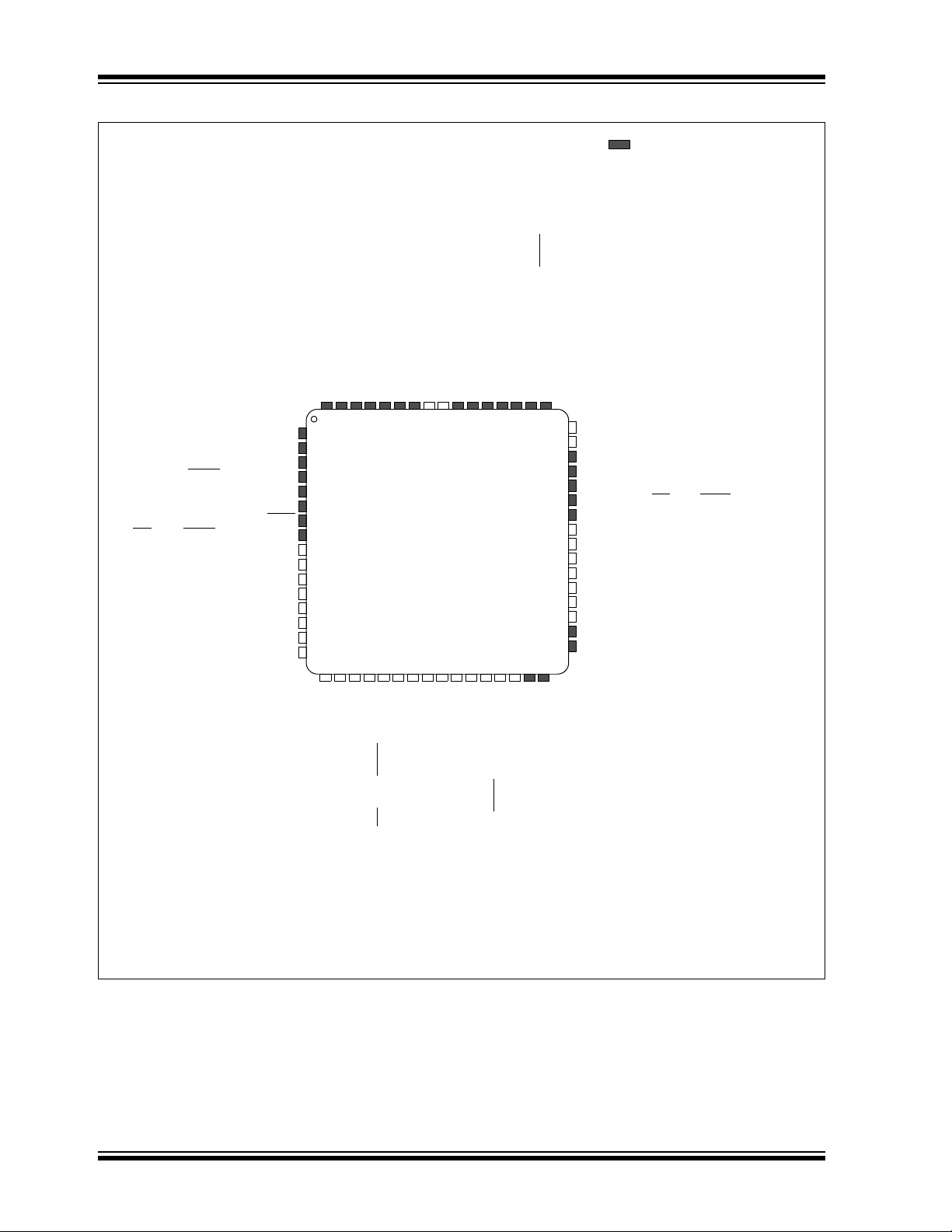
PIC32MX5XX/6XX/7XX
64-Pin TQFP
= Pins are up to 5V tolerant
PIC32MX675F512H
PIC32MX695F512H
PIC32MX675F256H
ETXEN/PMD5/RE5
ETXD0/PMD6/RE6
ETXD1/PMD7/RE7
SCK2/U6TX/U3RTS
/PMA5/CN8/RG6
V
DD
AN5/C1IN+/V
BUSON
/CN7/RB5
AN4/C1IN-/CN6/RB4
AN3/C2IN+/CN5/RB3
AN2/C2IN-/CN4/RB2
SDA4/SDI2/U3RX/PMA4/CN9/RG7
SCL4/SDO2/U3TX/PMA3/CN10/RG8
PGEC1/AN1/V
REF
-/CV
REF
-/CN3/RB1
PGED1/AN0/V
REF
+/CV
REF
+/PMA6/CN2/RB0
SS2
/U6RX/U3CTS/PMA2/CN11/RG9
MCLR
V
SS
64 63 62 61 60 59 58 57 56 55
3
4
5
7
8
9
10
11
1
2
6
54
14
15
16
12
13
53
52 51 50 49
AETXEN/ETXERR/CN15/RD6
PMRD/CN14/RD5
OC5/IC5/PMWR/CN13/RD4
SCL3/SDO3/U1TX/OC4/RD3
SDA3/SDI3/U1RX/ OC3/RD2
EMDIO/AEMDIO/SCK3/U4TX/U1RTS
/OC2/RD1
ERXERR/PMD4/RE4
ERXCLK/EREFCLK/PMD3/RE3
ERXDV/ECRSDV/PMD2/RE2
ERXD0/PMD1/RE1
AETXD1/ERXD3/RF0
V
CAP
/V
CORE
ERXD1/PMD0/RE0
AETXD0/ERXD2/RF1
ETXCLK/AERXERR/CN16/RD7
V
DD
22 23 24 25 26 27 28 29 30 31
40
39
38
37
36
35
34
33
42
41
32
43
17
18 19 20 21
45
44
47
46
48
AV
DD
AN8/SS4/U5RX/U2CTS/C1OUT/RB8
AN9/C2OUT/PMA7/RB9
TMS/AN10/CV
REFOUT
/PMA13/RB10
TDO/AN11/PMA12/RB11
V
DD
PGEC2/AN6/OCFA/RB6
PGED2/AN7/RB7
SCL5/SDO4/U2TX/PMA8/CN18/RF5
SDA5/SDI4/U2RX/PMA9/CN17/RF4
TCK/AN12/PMA11/RB12
TDI/AN13/PMA10/RB13
AN14/SCK4/U5TX/ U2RTS
/PMALH/PMA1/RB14
AN15/EMDC/AEMDC/OCFB/PMALL/PMA0/CN12/RB15
V
SS
AV
SS
SOSCI/CN1/RC13
OC1/INT0/RD0
ECOL/AECRSDV/SCL1/IC3/PMCS2/PMA15/INT3/RD10
AERXD0/ETXD2/SS3
/U4RX/U1CTS/SDA1/IC2/INT2/RD9
RTCC/AERXD1/ETXD3/I C1/INT1/RD8
ECRS/AEREFCLK/IC4/PMCS1/PMA14/INT4/RD11
OSC2/CLKO/RC15
OSC1/CLKI/RC12
V
DD
D+/RG2
V
USB
V
BUS
USBID/RF3
D-/RG3
SOSCO/T1CK/CN0/RC14
Vss
PIC32MX664F064H
PIC32MX664F128H
Pin Diagrams (Continued)
DS61156G-page 12 © 2009-2011 Microchip Technology Inc.
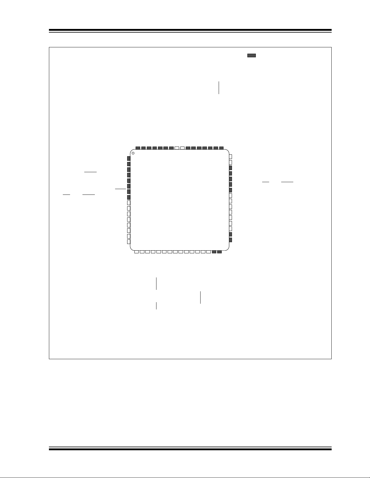
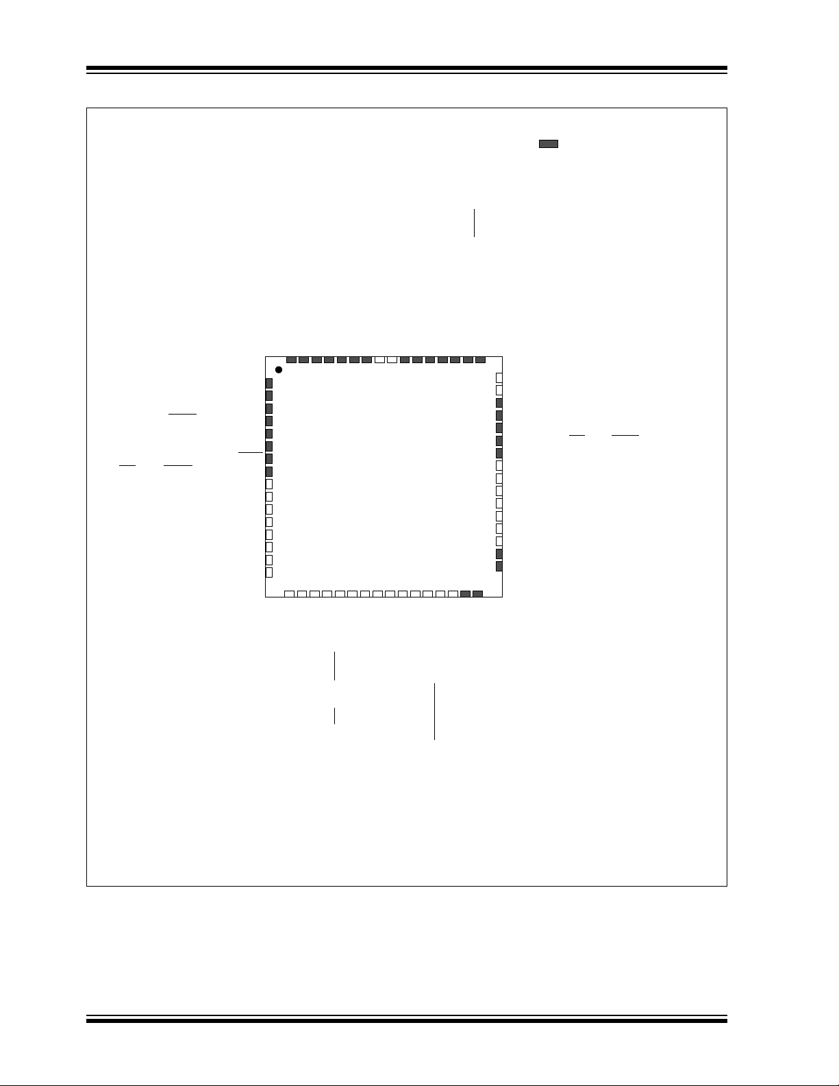
Pin Diagrams (Continued)
64-Pin TQFP
= Pins are up to 5V tolerant
PIC32MX795F512H
PIC32MX775F256H
PIC32MX775F512H
ETXEN/PMD5/RE5
ETXD0/PMD6/RE6
ETXD1/PMD7/RE7
SCK2/U6TX/U3RTS
/PMA5/CN8/RG6
V
DD
AN5/C1IN+/V
BUSON
/CN7/RB5
AN4/C1IN-/CN6/RB4
AN3/C2IN+/CN5/RB3
AN2/C2IN-/CN4/RB2
SDA4/SDI2/U3RX/PMA4/CN9/RG7
SCL4/SDO2/U3TX/PMA3/CN10/RG8
PGEC1/AN1/V
REF
-/CV
REF
-/CN3/RB1
PGED1/AN0/V
REF
+/CV
REF
+/PMA6/CN2/RB0
SS2
/U6RX/U3CTS/PMA2/CN11/RG9
MCLR
V
SS
64 63 62 61 60 59 58 57 56 55
3
4
5
7
8
9
10
11
1
2
6
54
14
15
16
12
13
53
52 51 50 49
AETXEN/ETXERR/CN15/RD6
PMRD/CN14/RD5
OC5/IC5/PMWR/CN13/RD4
SCL3/SDO3/U1TX/OC4/RD3
SDA3/SDI3/U1RX/OC3/RD2
EMDIO/AEMDIO/SCK3/U4TX/U1RTS
/OC2/RD1
ERXERR/PMD4/RE4
ERXCLK/EREFCLK/PMD3/RE3
ERXDV/ECRSDV/PMD2/RE2
ERXD0/PMD1/RE1
C1RX/AETXD1/ERXD3/RF0
V
CAP
/V
CORE
ERXD1/PMD0/RE0
C1TX/AETXD0/ERXD2/RF1
ETXCLK/AERXERR/CN16/RD7
V
DD
22 23 24 25 26 27 28 29 30 31
40
39
38
37
36
35
34
33
42
41
32
43
17
18 19 20 21
45
44
47
46
48
AV
DD
AN8/C2TX/SS4/U5RX/U2CTS/C1OUT/RB8
AN9/C2OUT/PMA7/RB9
TMS/AN10/CV
REFOUT
/PMA13/RB10
TDO/AN11/PMA12/RB11
V
DD
PGEC2/AN6/OCFA/RB6
PGED2/AN7/RB7
AC1RX/SCL5/SDO4/U2TX/PMA8/CN18/RF5
AC1TX/SDA5/SDI4/U2RX/PMA9/CN17/RF4
TCK/AN12/PMA11/RB12
TDI/AN13/PMA10/RB13
AN14/C2RX/SCK4/U5TX/U2RTS
/PMALH/PMA1/RB14
AN15/EMDC/AEMDC/OCFB/PMALL/PMA0/CN12/RB15
V
SS
AV
SS
SOSCI/CN1/RC13
OC1/INT0/RD0
ECOL/AECRSDV/SCL1/IC3/PMCS2/PMA15/INT3/RD10
AERXD0/ETXD2/SS3/U4RX/U1CTS/SDA1/IC2/INT2/RD9
RTCC/AERXD1/ETXD3/I C1/INT1/RD8
ECRS/AEREFCLK/IC4/PMCS1/PMA14/I NT4/RD11
OSC2/CLKO/RC15
OSC1/CLKI/RC12
V
DD
D+/RG2
V
USB
V
BUS
USBID/RF3
D-/RG3
SOSCO/T1CK/CN0/RC14
Vss
PIC32MX5XX/6XX/7XX
© 2009-2011 Microchip Technology Inc. DS61156G-page 13
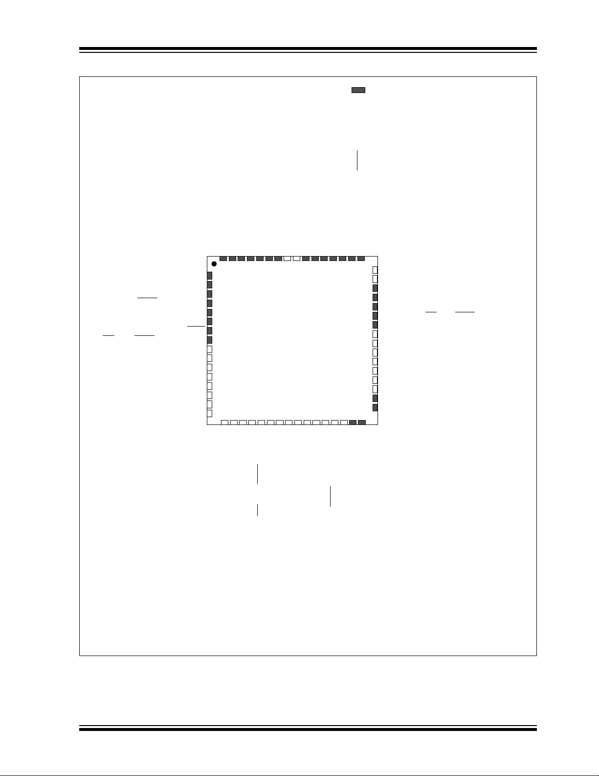
PIC32MX5XX/6XX/7XX
64-Pin TQFP
= Pins are up to 5V tolerant
PIC32MX764F128H
ETXEN/PMD5/RE5
ETXD0/PMD6/RE6
ETXD1/PMD7/RE7
SCK2/U6TX/U3RTS
/PMA5/CN8/RG6
V
DD
AN5/C1IN+/V
BUSON
/CN7/RB5
AN4/C1IN-/CN6/RB4
AN3/C2IN+/CN5/RB3
AN2/C2IN-/CN4/RB2
SDA4/SDI2/U3RX/PMA4/CN9/RG7
SCL4/SDO2/U3TX/PMA3/CN10/RG8
PGEC1/AN1/V
REF
-/CV
REF
-/CN3/RB1
PGED1/AN0/V
REF
+/CV
REF
+/PMA6/CN2/RB0
SS2
/U6RX/U3CTS/PMA2/CN11/RG9
MCLR
V
SS
64 63 62 61 60 59 58 57 56 55
3
4
5
7
8
9
10
11
1
2
6
54
14
15
16
12
13
53
52 51 50 49
AETXEN/ETXERR/CN15/RD6
PMRD/CN14/RD5
OC5/IC5/PMWR/CN13/RD4
SCL3/SDO3/U1TX/OC4/RD3
SDA3/SDI3/U1RXU1RX/OC3/RD2
EMDIO/AEMDIO/SCK3/U4TX/U1RTS
/OC2/RD1
ERXERR/PMD4/RE4
ERXCLK/EREFCLK/PMD3/RE3
ERXDV/ECRSDV/PMD2/RE2
ERXD0/PMD1/RE1
C1RX/AETXD1/ERXD3/RF0
V
CAP
/V
CORE
ERXD1/PMD0/RE0
C1TX/AETXD0/ERXD2/RF1
ETXCLK/AERXERR/CN16/RD7
V
DD
22 23 24 25 26 27 28 29 30 31
40
39
38
37
36
35
34
33
42
41
32
43
17
18 19 20 21
45
44
47
46
48
AV
DD
AN8/SS4/U5RX/U2CTS/C1OUT/RB8
AN9/C2OUT/PMA7/RB9
TMS/AN10/CV
REFOUT
/PMA13/RB10
TDO/AN11/PMA12/RB11
V
DD
PGEC2/AN6/OCFA/RB6
PGED2/AN7/RB7
AC1RX/SCL5/SDO4/U2TX/PMA8/CN18/RF5
AC1TX/SDA5/SDI4/U2RX/PMA9/CN17/RF4
TCK/AN12/PMA11/RB12
TDI/AN13/PMA10/RB13
AN14/SCK4/U5TX/U2RTS
/PMALH/PMA1/RB14
AN15/EMDC/AEMDC/OCFB/PMALL/PMA0/CN12/RB15
V
SS
AV
SS
SOSCI/CN1/RC13
OC1/INT0/RD0
ECOL/AECRSDV/SCL1/IC3/PMCS2/PMA15/INT3/RD10
AERXD0/ETXD2/SS3/U4RX/U1CTS/SDA1/IC2/INT2/RD9
RTCC/AERXD1/ETXD3/I C1/INT1/RD8
ECRS/AEREFCLK/IC4/PMCS1/PMA14/I NT4/RD11
OSC2/CLKO/RC15
OSC1/CLKI/RC12
V
DD
D+/RG2
V
USB
V
BUS
USBID/RF3
D-/RG3
SOSCO/T1CK/CN0/RC14
Vss
Pin Diagrams (Continued)
DS61156G-page 14 © 2009-2011 Microchip Technology Inc.
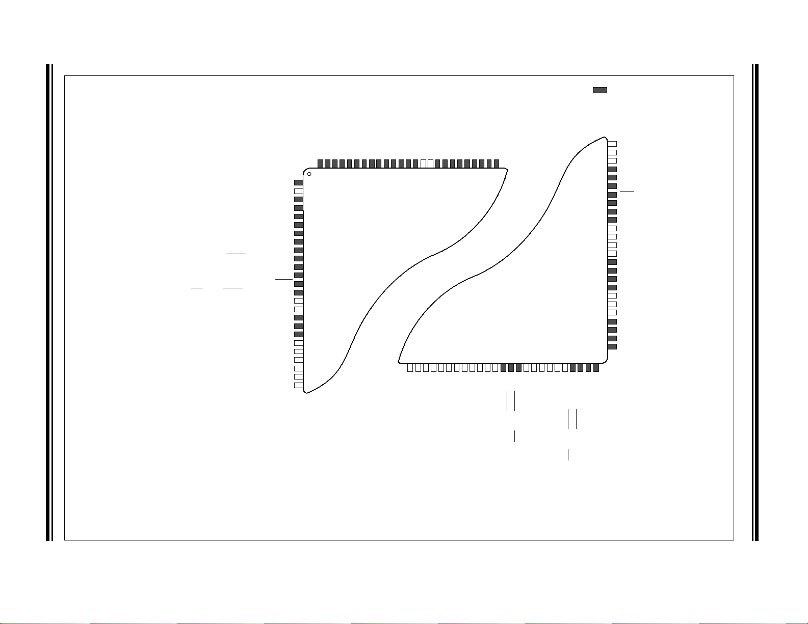
Pin Diagrams (Continued)
PMRD/CN14/RD5
OC5/PMWR/CN13/RD4
PMD13/CN19/RD13
IC5/PMD12/RD12
OC4/RD3
OC3/RD2
OC2/RD1
TRD3/RA7
TRCLK/RA6
PMD2/RE2
TRD0/RG13
TRD1/RG12
TRD2/RG14
PMD1/RE1
PMD0/RE0
PMD8/RG0
PMD4/RE4
PMD3/RE3
C1RX/PMD11/RF0
SOSCI/CN1/RC13
SDO1/OC1/INT0/RD0
SCK1/IC3/PMCS2/PMA15/RD10
SS1/
IC2
/RD9
RTCC/IC1/RD8
IC4/PMCS1/PMA14/RD11
SDA1/INT4/RA15
SCL1/INT3/RA14
OSC2/CLKO/RC15
OSC1/CLKI/RC12
V
DD
D+/RG2
V
USB
V
BUS
SCL3/SDO3/U1TX/RF8
D-/RG3
SDA3/SDI3/U1RX/RF2
USBID/RF3
V
SS
SOSCO/T1CK/CN0/RC14
V
REF
+/CV
REF
+/PMA6/RA10
V
REF
-/CV
REF
-/PMA7/RA9
AV
DD
AV
SS
AN8/C1OUT/RB8
AN9/C2OUT/RB9
AN10/CV
REFOUT
/PMA13/RB10
AN11/PMA12/RB11
V
DD
AC1RX/SS4/U5RX/U2CTS/RF12
AC1TX/SCK4/U5TX/U2RTS
/RF13
SS3
/U4RX/U1CTS/CN20/RD14
SCK3/U4TX/U1RTS
/CN21/RD15
V
DD
V
SS
PGEC2/AN6/OCFA/RB6
PGED2/AN7/RB7
SCL5/SDO4/U2TX/PMA8/CN18/RF5
SDA5/SDI4/U2RX/PMA9/CN17/RF4
PMD5/RE5
PMD6/RE6
PMD7/RE7
T2CK/RC1
T3CK/RC2
T4CK/RC3
T5CK/SDI1/RC4
SCK2/U6TX/U3RTS
/PMA5/CN8/RG6
V
DD
TMS/RA0
INT1/RE8
INT2/RE9
AN5/C1IN+/V
BUSON
/CN7/RB5
AN4/C1IN-/CN6/RB4
AN3/C2IN+/CN5/RB3
AN2/C2IN-/CN4/RB2
SDA4/SDI2/U3RX/PMA4/CN9/RG7
SCL4/SDO2/U3TX/PMA3/CN10/RG8
PGEC1/AN1/CN3/RB1
PGED1/AN0/CN2/RB0
V
DD
RG15
SS2
/U6RX/U3CTS
/PMA2/CN11/RG9
MCLR
AN12/PMA11/RB12
AN13/PMA10/RB13
AN14/PMALH/PMA1/RB14
AN15/OCFB/PMALL/PMA0/CN12/RB15
PMD9/RG1
C1TX/PMD10/RF1
V
DD
PMD14/CN15/RD6
TDO/RA5
SDA2/RA3
SCL2/RA2
V
SS
V
SS
V
SS
V
CAP
/V
CORE
TDI/RA4
TCK/RA1
100-Pin TQFP
PMD15/CN16/RD7
= Pins are up to 5V tolerant
20
2
3
4
5
6
7
8
9
10
11
12
13
14
15
16
65
64
63
62
61
60
59
56
45
44
43
42
41
40
39
2829303132333435363738
17
18
19
21
22
1
72
71
70
69
68
67
66
75
74
73
58
57
24
23
25
27
464748
49
55
54
53
52
51
50
26
PIC32MX575F512L
92949391908988878685848382818079789576
77
969897
99
100
PIC32MX575F256L
PIC32MX534F064L
PIC32MX564F064L
PIC32MX564F128L
PIC32MX5XX/6XX/7XX
© 2009-2011 Microchip Technology Inc. DS61156G-page 15
DS61156G-page 16 © 2009-2011 Microchip Technology Inc.
100-Pin TQFP
PIC32MX675F512L
PIC32MX695F512L
PIC32MX675F256L
= Pins are up to 5V tolerant
PMRD/CN14/RD5
OC5/PMWR/CN13/RD4
ETXD3/PMD13/CN19/RD13
ETXD2/IC5/PMD12/RD12
OC4/RD3
OC3/RD2
OC2/RD1
TRD3/RA7
TRCLK/RA6
PMD2/RE2
TRD0/RG13
TRD1/RG12
TRD2/RG14
PMD1/RE1
PMD0/RE0
PMD8/RG0
PMD4/RE4
PMD3/RE3
ETXD1/PMD11/RF0
PMD5/RE5
PMD6/RE6
PMD7/RE7
T2CK/RC1
T3CK/RC2
T4CK/RC3
T5CK/SDI1/RC4
ECOL/SCK2/U6TX/U3RTS
/PMA5/CN8/RG6
V
DD
TMS/RA0
AERXD0/INT1/RE8
AERXD1/INT2/RE9
AN5/C1IN+/V
BUSON
/CN7/RB5
AN4/C1IN-/CN6/RB4
AN3/C2IN+/CN5/RB3
AN2/C2IN-/CN4/RB2
ECRS/SDA4/SDI2/U3RX/PMA4/CN9/RG7
ERXDV/AERXDV/ECRSDV/AECRSDV/SCL4/SDO2/U3TX/PMA3/CN10/RG8
PGEC1/AN1/CN3/RB1
PGED1/AN0/CN2/RB0
V
DD
AERXERR/RG15
ERXCLK/AERXCLK/EREFCLK/AEREFCLK/SS2
/U6RX/U3CTS/PMA2/CN11/RG9
MCLR
ETXERR/PMD9/RG1
ETXD0/PMD10/RF1
VDDETXEN/PMD14/CN15/RD6
V
SS
V
CAP
/V
DDCORE
ETXCLK/PMD15/CN16/RD7
20
2
3
4
5
6
7
8
9
10
11
12
13
14
15
16
17
18
19
21
22
1
24
23
25
92949391908988878685848382818079789576
77
969897
99
100
SOSCI/CN1/RC13
SDO1/OC1/INT0/RD0
SS1/
IC2/RD9
RTCC/EMDIO/AEMDIO/IC1/RD8
EMDC/AEMDC/IC4/PMCS1/PMA14/RD11
AETXEN/SDA1/INT4/RA15
AETXCLK/SCL1/INT3/RA14
OSC2/CLKO/RC15
OSC1/CLKI/RC12
V
DD
D+/RG2
V
USB
V
BUS
SCL3/SDO3/U1TX/RF8
D-/RG3
SDA3/SDI3/U1RX/RF2
USBID/RF3
V
SS
SOSCO/T1CK/CN0/RC14
V
REF
+/CV
REF
+/AERXD3/PMA6/RA10
V
REF
-/CV
REF
-/AERXD2/PMA7/RA9
AV
DD
AV
SS
AN8/C1OUT/RB8
AN9/C2OUT/RB9
AN10/CV
REFOUT
/PMA13/RB10
AN11/ERXERR/AETXERR/PMA12/RB11
V
DD
SS4/U5RX/U2CTS/RF12
SCK4/U5TX/U2RTS
/RF13
AETXD0/SS3
/U4RX/U1CTS/CN20/RD14
AETXD1/SCK3/U4TX/U1RTS
/CN21/RD15
V
DD
V
SS
PGED2/AN7/RB7
SCL5/SDO4/U2TX/PMA8/CN18/RF5
SDA5/SDI4/U2RX/PMA9/CN17/RF4
AN12/ERXD0/AECRS/PMA11/RB12
AN13/ERXD1/AECOL/PMA10/RB13
AN14/ERXD2/AETXD3/PMALH/PMA1/RB14
AN15/ERXD3/AETXD2/OCFB/PMALL/PMA0/CN12/RB15
TDO/RA5
SDA2/RA3
SCL2/RA2
V
SS
V
SS
TDI/RA4
TCK/RA1
65
64
63
62
61
60
59
56
45
44
43
42
41
40
39
2829303132333435363738
72
71
70
69
68
67
66
75
74
73
58
57
27
464748
49
55
54
53
52
51
50
SCK1/IC3/PMCS2/PMA15/RD10
PIC32MX664F064L
PIC32MX664F128L
PGEC2/AN6/OCFA/RB6
26
Pin Diagrams (Continued)
PIC32MX5XX/6XX/7XX
© 2009-2011 Microchip Technology Inc. DS61156G-page 17
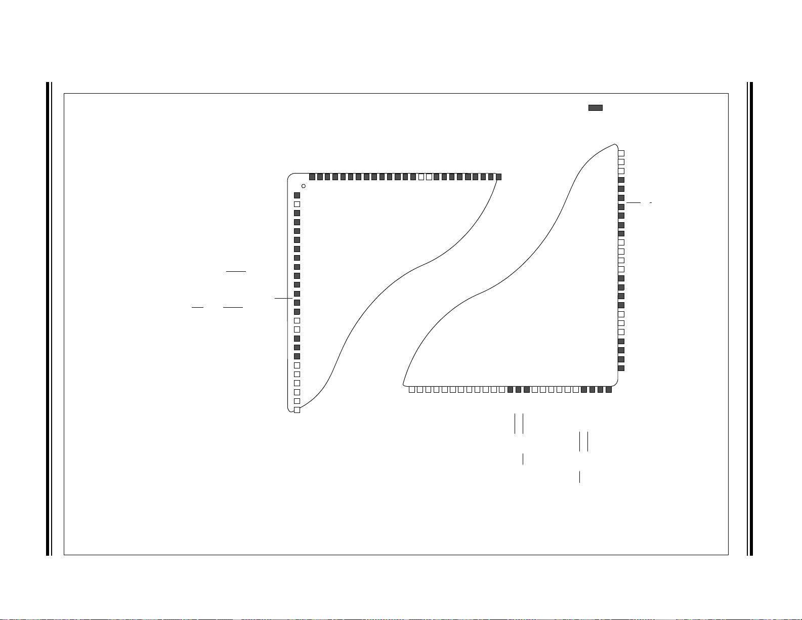
100-Pin TQFP
= Pins are up to 5V tolerant
PIC32MX795F512L
PIC32MX775F256L
PIC32MX775F512L
PMRD/CN14/RD5
OC5/PMWR/CN13/RD4
ETXD3/PMD13/CN19/RD13
ETXD2/IC5/PMD12/RD12
OC4/RD3
OC3/RD2
OC2/RD1
TRD3/RA7
TRCLK/RA6
PMD2/RE2
TRD0/RG13
TRD1/RG12
TRD2/RG14
PMD1/RE1
PMD0/RE0
C2RX/PMD8/RG0
PMD4/RE4
PMD3/RE3
C1RX/ETXD1/PMD11/RF0
PMD5/RE5
PMD6/RE6
PMD7/RE7
T2CK/RC1
T3CK/AC2TX/RC2
T4CK/AC2RX/RC3
T5CK/SDI1/RC4
ECOL/SCK2/U6TX/U3RTS
/PMA5/CN8/RG6
V
DD
TMS/RA0
AERXD0/INT1/RE8
AERXD1/INT2/RE9
AN5/C1IN+/V
BUSON
/CN7/RB5
AN4/C1IN-/CN6/RB4
AN3/C2IN+/CN5/RB3
AN2/C2IN-/CN4/RB2
ECRS/SDA4/SDI2/U3RX/PMA4/CN9/RG7
ERXDV/AERXDV/ECRSDV/AECRSDV/SCL4/SDO2/U3TX/PMA3/CN10/RG8
PGEC1/AN1/CN3/RB1
PGED1/AN0/CN2/RB0
V
DD
AERXERR/RG15
ERXCLK/AERXCLK/EREFCLK/AEREFCLK/SS2
/U6RX/U3CTS/PMA2/CN11/RG9
MCLR
C2TX/ETXERR/PMD9/RG1
C1TX/ETXD0/PMD10/RF1
VDDETXEN/PMD14/CN15/RD6
V
SS
V
CAP
/V
DDCORE
ETXCLK/PMD15/CN16/RD7
20
2
3
4
5
6
7
8
9
10
11
12
13
14
15
16
17
18
19
21
22
1
24
23
25
92949391908988878685848382818079789576
77
969897
99
100
SOSCI/CN1/RC13
SDO1/OC1/INT0/RD0
SCK1/IC3/PMCS2/PMA15/RD10
SS1/
IC2/RD9
RTCC/EMDIO/AEMDIO/IC1/RD8
EMDC/AEMDC/IC4/PMCS1/PMA14/RD1
AETXEN/SDA1/INT4/RA15
AETXCLK/SCL1/INT3/RA14
OSC2/CLKO/RC15
OSC1/CLKI/RC12
V
DD
D+/RG2
V
USB
V
BUS
SCL3/SDO3/U1TX/RF8
D-/RG3
SDA3/SDI3/U1RX/RF2
USBID/RF3
V
SS
SOSCO/T1CK/CN0/RC14
V
REF
+/CV
REF
+/AERXD3/PMA6/RA10
V
REF
-/CV
REF
-/AERXD2/PMA7/RA9
AV
DD
AV
SS
AN8/C1OUT/RB8
AN9/C2OUT/RB9
AN10/CV
REFOUT
/PMA13/RB10
AN11/ERXERR/AETXERR/PMA12/RB11
V
DD
AC1RX/SS4/U5RX/U2CTS/RF12
AC1TX/SCK4/U5TX/U2RTS
/RF13
AETXD0/SS3
/U4RX/U1CTS/CN20/RD14
AETXD1/SCK3/U4TX/U1RTS
/CN21/RD15
V
DD
V
SS
PGEC2/AN6/OCFA/RB6
PGED2/AN7/RB7
SCL5/SDO4/U2TX/PMA8/CN18/RF5
SDA5/SDI4/U2RX/PMA9/CN17/RF4
AN12/ERXD0/AECRS/PMA11/RB12
AN13/ERXD1/AECOL/PMA10/RB13
AN14/ERXD2/AETXD3/PMALH/PMA1/RB14
AN15/ERXD3/AETXD2/OCFB/PMALL/PMA0/CN12/RB15
TDO/RA5
SDA2/RA3
SCL2/RA2
V
SS
V
SS
TDI/RA4
TCK/RA1
65
64
63
62
61
60
59
56
45
44
43
42
41
40
39
2829303132333435363738
72
71
70
69
68
67
66
75
74
73
58
57
27
464748
49
55
54
53
52
51
50
26
Pin Diagrams (Continued)
PIC32MX5XX/6XX/7XX
DS61156G-page 18 © 2009-2011 Microchip Technology Inc.
100-Pin TQFP
= Pins are up to 5V tolerant
PIC32MX764F128L
PMRD/CN14/RD5
OC5/PMWR/CN13/RD4
ETXD3/PMD13/CN19/RD13
ETXD2/IC5/PMD12/RD12
OC4/RD3
OC3/RD2
OC2/RD1
TRD3/RA7
TRCLK/RA6
PMD2/RE2
TRD0/RG13
TRD1/RG12
TRD2/RG14
PMD1/RE1
PMD0/RE0
PMD8/RG0
PMD4/RE4
PMD3/RE3
C1RX/ETXD1/PMD11/RF0
PMD5/RE5
PMD6/RE6
PMD7/RE7
T2CK/RC1
T3CK/RC2
T4CK/RC3
T5CK/SDI1/RC4
ECOL/SCK2/U6TX/U3RTS
/PMA5/CN8/RG6
V
DD
TMS/RA0
AERXD0/INT1/RE8
AERXD1/INT2/RE9
AN5/C1IN+/V
BUSON
/CN7/RB5
AN4/C1IN-/CN6/RB4
AN3/C2IN+/CN5/RB3
AN2/C2IN-/CN4/RB2
ECRS/SDA4/SDI2/U3RX/PMA4/CN9/RG7
ERXDV/AERXDV/ECRSDV/AECRSDV/SCL4/SDO2/U3TX/PMA3/CN10/RG8
PGEC1/AN1/CN3/RB1
PGED1/AN0/CN2/RB0
V
DD
AERXERR/RG15
ERXCLK/AERXCLK/EREFCLK/AEREFCLK/SS2
/U6RX/U3CTS/PMA2/CN11/RG9
MCLR
ETXERR/PMD9/RG1
C1TX/ETXD0/PMD10/RF1
VDDETXEN/PMD14/CN15/RD6
V
SS
V
CAP
/V
DDCORE
ETXCLK/PMD15/CN16/RD7
20
2
3
4
5
6
7
8
9
10
11
12
13
14
15
16
17
18
19
21
22
1
24
23
25
92949391908988878685848382818079789576
77
969897
99
100
SOSCI/CN1/RC13
SDO1/OC1/INT0/RD0
SCK1/IC3/PMCS2/PMA15/RD10
SS1/
IC2/RD9
RTCC/EMDIO/AEMDIO/IC1/RD8
EMDC/AEMDC/IC4/PMCS1/PMA14/RD1
AETXEN/SDA1/INT4/RA15
AETXCLK/SCL1/INT3/RA14
OSC2/CLKO/RC15
OSC1/CLKI/RC12
V
DD
D+/RG2
V
USB
V
BUS
SCL3/SDO3/U1TX/RF8
D-/RG3
SDA3/SDI3/U1RX/RF2
USBID/RF3
V
SS
SOSCO/T1CK/CN0/RC14
V
REF
+/CV
REF
+/AERXD3/PMA6/RA10
V
REF
-/CV
REF
-/AERXD2/PMA7/RA9
AV
DD
AV
SS
AN8/C1OUT/RB8
AN9/C2OUT/RB9
AN10/CV
REFOUT
/PMA13/RB10
AN11/ERXERR/AETXERR/PMA12/RB11
V
DD
AC1RX/SS4/U5RX/U2CTS/RF12
AC1TX/SCK4/U5TX/U2RTS
/RF13
AETXD0/SS3
/U4RX/U1CTS/CN20/RD14
AETXD1/SCK3/U4TX/U1RTS
/CN21/RD15
V
DD
V
SS
PGEC2/AN6/OCFA/RB6
PGED2/AN7/RB7
SCL5/SDO4/U2TX/PMA8/CN18/RF5
SDA5/SDI4/U2RX/PMA9/CN17/RF4
AN12/ERXD0/AECRS/PMA11/RB12
AN13/ERXD1/AECOL/PMA10/RB13
AN14/ERXD2/AETXD3/PMALH/PMA1/RB14
AN15/ERXD3/AETXD2/OCFB/PMALL/PMA0/CN12/RB15
TDO/RA5
SDA2/RA3
SCL2/RA2
V
SS
V
SS
TDI/RA4
TCK/RA1
65
64
63
62
61
60
59
56
45
44
43
42
41
40
39
2829303132333435363738
72
71
70
69
68
67
66
75
74
73
58
57
27
464748
49
55
54
53
52
51
50
26
Pin Diagrams (Continued)
PIC32MX5XX/6XX/7XX
Pin Diagrams (Continued)
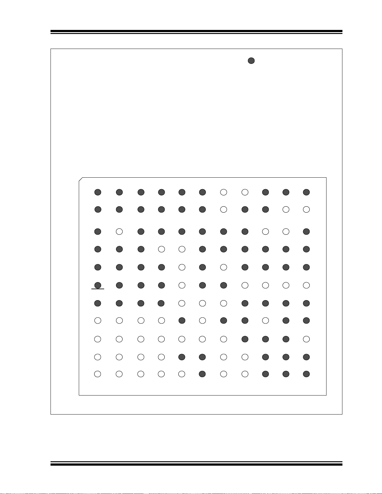
121-Pin XBGA
(1)
1234567891011
A
RE4 RE3 RG13 RE0 RG0 RF1 VDD VSS RD12 RD2 RD1
B
NC RG15 RE2 RE1 RA7 RF0 VCAP/
V
CORE
RD5 RD3 VSS RC14
C
RE6 VDD RG12 RG14 RA6 NC RD7 RD4 VDD RC13 RD11
D
RC1 RE7 RE5 VSS VSS NC RD6 RD13 RD0 NC RD10
E
RC4 RC3 RG6 RC2 VDD RG1 VSS RA15 RD8 RD9 RA14
F
MCLR RG8 RG9 RG7 VSS NC NC VDD RC12 VSS RC15
G
RE8 RE9 RA0 NC VDD VSS VSS NC RA5 RA3 RA4
H
RB5 RB4 VSS VDD NC VDD NC VBUS VUSB RG2 RA2
J
RB3 RB2 RB7 AVDD RB11 RA1 RB12 NC NC RF8 RG3
K
RB1 RB0 RA10 RB8 NC RF12 RB14 VDD RD15 RF3 RF2
L
RB6 RA9 AVSS RB9 RB10
RF13
RB13 RB15 RD14 RF4 RF5
PIC32MX575F256L
Note 1: Refer to Table 4, Tab l e 5 and Ta bl e 6 for full pin names.
= Pins are up to 5V tolerant
PIC32MX795F512L
PIC32MX575F512L
PIC32MX675F512L
PIC32MX695F512L
PIC32MX675F256L
PIC32MX775F256L
PIC32MX775F512L
PIC32MX534F064L
PIC32MX564F064L
PIC32MX564F128L
PIC32MX664F064L
PIC32MX664F128L
PIC32MX764F128L
PIC32MX5XX/6XX/7XX
© 2009-2011 Microchip Technology Inc. DS61156G-page 19
PIC32MX5XX/6XX/7XX
TABLE 4: PIN NAMES: PIC32MX534F064L, PIC32MX564F064L, PIC32MX564F128L,
PIC32MX575F256L AND PIC32MX575F512L DEVICES
Pin
Number
Full Pin Name
A1 PMD4/RE4 E8 SDA1/INT4/RA15
A2 PMD3/RE3 E9 RTCC/IC1/RD8
A3 TRD0/RG13 E10 SS1
A4 PMD0/RE0 E11 SCL1/INT3/RA14
A5 PMD8/RG0 F1 MCLR
A6 C1TX/PMD10/RF1 F2 SCL4/SDO2/U3TX/PMA3/CN10/RG8
A7 V
A8 V
DD F3 SS2/U6RX/U3CTS/PMA2/CN11/RG9
SS F4 SDA4/SDI2/U3RX/PMA4/CN9/RG7
A9 IC5/PMD12/RD12 F5 V
A10 OC3/RD2 F6 No Connect (NC)
A11 OC2/RD1 F7 No Connect (NC)
B1 No Connect (NC) F8 V
B2 RG15 F9 OSC1/CLKI/RC12
B3 PMD2/RE2 F10 V
B4 PMD1/RE1 F11 OSC2/CLKO/RC15
B5 TRD3/RA7 G1 INT1/RE8
B6 C1RX/PMD11/RF0 G2 INT2/RE9
B7 V
CAP/VCORE G3 TMS/RA0
B8 PMRD/CN14/RD5 G4 No Connect (NC)
B9 OC4/RD3 G5 V
B10 VSS G6 VSS
B11 SOSCO/T1CK/CN0/RC14 G7 VSS
C1 PMD6/RE6 G8 No Connect (NC)
C2 V
DD G9 TDO/RA5
C3 TRD1/RG12 G10 SDA2/RA3
C4 TRD2/RG14 G11 TDI/RA4
C5 TRCLK/RA6 H1 AN5/C1IN+/V
C6 No Connect (NC) H2 AN4/C1IN-/CN6/RB4
C7 PMD15/CN16/RD7 H3 V
C8 OC5/PMWR/CN13/RD4 H4 VDD
C9 VDD H5 No Connect (NC)
C10 SOSCI/CN1/RC13 H6 V
C11 IC4/PMCS1/PMA14/RD11 H7 No Connect (NC)
D1 T2CK/RC1 H8 V
D2 PMD7/RE7 H9 VUSB
D3 PMD5/RE5 H10 D+/RG2
D4 V
D5 V
SS H11 SCL2/RA2
SS J1 AN3/C2IN+/CN5/RB3
D6 No Connect (NC) J2 AN2/C2IN-/CN4/RB2
D7 PMD14/CN15/RD6 J3 PGED2/AN7/RB7
D8 PMD13/CN19/RD13 J4 AV
D9 SDO1/OC1/INT0/RD0 J5 AN11/PMA12/RB11
D10 No Connect (NC) J6 TCK/RA1
D11 SCK1/IC3/PMCS2/PMA15/RD10 J7 AN12/PMA11/RB12
E1 T5CK/SDI1/RC4 J8 No Connect (NC)
E2 T4CK/RC3 J9 No Connect (NC)
E3 SCK2/U6TXU6TX/U3RTS
/PMA5/CN8/RG6 J10 SCL3/SDO3/U1TX/RF8
E4 T3CK/RC2 J11 D-/RG3
E5 V
DD K1 PGEC1/AN1/CN3/RB1
E6 PMD9/RG1 K2 PGED1/AN0/CN2/RB0
E7 V
SS K3 VREF+/CVREF+/PMA6/RA10
Pin
Number
Full Pin Name
/IC2/RD9
SS
DD
SS
DD
BUSON/CN7/RB5
SS
DD
BUS
DD
DS61156G-page 20 © 2009-2011 Microchip Technology Inc.

PIC32MX5XX/6XX/7XX
TABLE 4: PIN NAMES: PIC32MX534F064L, PIC32MX564F064L, PIC32MX564F128L,
PIC32MX575F256L AND PIC32MX575F512L DEVICES (CONTINUED)
Pin
Number
K4 AN8/C1OUT/RB8 L3 AVSS
K5 No Connect (NC) L4 AN9/C2OUT/RB9
K6 AC1RX/SS4
K7 AN14/PMALH/PMA1/RB14 L6 AC1TX/SCK4/U5TX/U2RTS
K8 V
K9 SCK3/U4TX/U1RTS
K10 USBID/RF3 L9 SS3
K11 SDA3/SDI3/U1RX/RF2 L10 SDA5/SDI4/U2RX/PMA9/CN17/RF4
L1 PGEC2/AN6/OCFA/RB6 L11 SCL5/SDO4/U2TX/PMA8/CN18/RF5
L2 V
DD L7 AN13/PMA10/RB13
REF-/CVREF-/PMA7/RA9
Full Pin Name
/U5RX/U2CTS/RF12 L5 AN10/CVREFOUT/PMA13/RB10
/CN21/RD15 L8 AN15/OCFB/PMALL/PMA0/CN12/RB15
Pin
Number
Full Pin Name
/RF13
/U4RX/U1CTS/CN20/RD14
© 2009-2011 Microchip Technology Inc. DS61156G-page 21
PIC32MX5XX/6XX/7XX
TABLE 5: PIN NAMES: PIC32MX664F064L, PIC32MX664F128L, PIC32MX675F256L,
PIC32MX675F512L AND PIC32MX695F512L DEVICES
Pin
Number
Full Pin Name
A1 PMD4/RE4 E8 AETXEN/SDA1/INT4/RA15
A2 PMD3/RE3 E9 RTCC/EMDIO/AEMDIO/IC1/RD8
A3 TRD0/RG13 E10 SS1
A4 PMD0/RE0 E11 AETXCLK/SCL1/INT3/RA14
A5 PMD8/RG0 F1 MCLR
A6 ETXD0/PMD10/RF1 F2 ERXDV/AERXDV/ECRSDV/AECRSDV//SCL4/SDO2/
DD F3 ERXCLK/AERXCLK/EREFCLK/AEREFCLK//SS2/U6RX/
A7 V
SS F4 ECRS/SDA4/SDI2/U3RX/PMA4/CN9/RG7
A8 V
A9 ETXD2/IC5/PMD12/RD12 F5 V
A10 OC3/RD2 F6 No Connect (NC)
A11 OC2/RD1 F7 No Connect (NC)
B1 No Connect (NC) F8 V
B2 AERXERR/RG15 F9 OSC1/CLKI/RC12
B3 PMD2/RE2 F10 V
B4 PMD1/RE1 F11 OSC2/CLKO/RC15
B5 TRD3/RA7 G1 AERXD0/INT1/RE8
B6 ETXD1/PMD11/RF0 G2 AERXD1/INT2/RE9
CAP/VCORE G3 TMS/RA0
B7 V
B8 PMRD/CN14/RD5 G4 No Connect (NC)
B9 OC4/RD3 G5 V
B10 VSS G6 VSS
B11 SOSCO/T1CK/CN0/RC14 G7 VSS
C1 PMD6/RE6 G8 No Connect (NC)
DD G9 TDO/RA5
C2 V
C3 TRD1/RG12 G10 SDA2/RA3
C4 TRD2/RG14 G11 TDI/RA4
C5 TRCLK/RA6 H1 AN5/C1IN+/V
C6 No Connect (NC) H2 AN4/C1IN-/CN6/RB4
C7 ETXCLK/PMD15/CN16/RD7 H3 V
C8 OC5/PMWR/CN13/RD4 H4 VDD
C9 VDD H5 No Connect (NC)
C10 SOSCI/CN1/RC13 H6 V
C11 EMDC/AEMDC/IC4/PMCS1/PMA14/RD11 H7 No Connect (NC)
D1 T2CK/RC1 H8 V
D2 PMD7/RE7 H9 VUSB
D3 PMD5/RE5 H10 D+/RG2
SS H11 SCL2/RA2
D4 V
SS J1 AN3/C2IN+/CN5/RB3
D5 V
D6 No Connect (NC) J2 AN2/C2IN-/CN4/RB2
D7 ETXEN/PMD14/CN15/RD6 J3 PGED2/AN7/RB7
D8 ETXD3/PMD13/CN19/RD13 J4 AV
D9 SDO1/OC1/INT0/RD0 J5 AN11/ERXERR/AETXERR/PMA12/RB11
D10 No Connect (NC) J6 TCK/RA1
D11 SCK1/IC3/PMCS2/PMA15/RD10 J7 AN12/ERXD0/AECRS/PMA11/RB12
E1 T5CK/SDI1/RC4 J8 No Connect (NC)
E2 T4CK/RC3 J9 No Connect (NC)
E3 ECOL/SCK2/U6TX/U3RTS
/PMA5/CN8/RG6 J10 SCL3/SDO3/U1TX/RF8
E4 T3CK/RC2 J11 D-/RG3
DD K1 PGEC1/AN1/CN3/RB1
E5 V
E6 ETXERR/PMD9/RG1 K2 PGED1/AN0/CN2/RB0
SS K3 VREF+/CVREF+/AERXD3/PMA6/RA10
E7 V
Pin
Number
/IC2/RD9
U3TX/PMA3/CN10/RG8
/PMA2/CN11/RG9
U3CTS
SS
DD
SS
DD
BUSON/CN7/RB5
SS
DD
BUS
DD
Full Pin Name
DS61156G-page 22 © 2009-2011 Microchip Technology Inc.
PIC32MX5XX/6XX/7XX
TABLE 5: PIN NAMES: PIC32MX664F064L, PIC32MX664F128L, PIC32MX675F256L,
PIC32MX675F512L AND PIC32MX695F512L DEVICES (CONTINUED)
Pin
Number
K4 AN8/C1OUT/RB8 L3 AVSS
K5 No Connect (NC) L4 AN9/C2OUT/RB9
K6 SS4
K7 AN14/ERXD2/AETXD3/PMALH/PMA1/RB14 L6 SCK4/U5TX/U2RTS
K8 V
K9 AETXD1/SCK3/U4TX/U1RTS
K10 USBID/RF3 L9 AETXD0/SS3
K11 SDA3/SDI3/U1RX/RF2 L10 SDA5/SDI4/U2RX/PMA9/CN17/RF4
L1 PGEC2/AN6/OCFA/RB6 L11 SCL5/SDO4/U2TX/PMA8/CN18/RF5
L2 V
/U5RX/U2CTS/RF12 L5 AN10/CVREFOUT/PMA13/RB10
DD L7 AN13/ERXD1/AECOL/PMA10/RB13
REF-/CVREF-/AERXD2/PMA7/RA9
Full Pin Name
/CN21/RD15 L8 AN15/ERXD3/AETXD2/OCFB/PMALL/PMA0/CN12/RB15
Pin
Number
Full Pin Name
/RF13
/U4RX/U1CTS/CN20/RD14
© 2009-2011 Microchip Technology Inc. DS61156G-page 23

PIC32MX5XX/6XX/7XX
TABLE 6: PIN NAMES: PIC32MX775F256L, PIC32MX775F512L AND
PIC32MX795F512L DEVICES
Pin
Number
Full Pin Name
A1 PMD4/RE4 E8 AETXEN/SDA1/INT4/RA15
A2 PMD3/RE3 E9 RTCC/EMDIO/AEMDIO/IC1/RD8
A3 TRD0/RG13 E10 SS1
A4 PMD0/RE0 E11 AETXCLK/SCL1/INT3/RA14
A5 C2RX/PMD8/RG0 F1 MCLR
A6 C1TX/ETXD0/PMD10/RF1 F2 ERXDV/AERXDV/ECRSDV/AECRSDV/SCL4/SDO2/
DD F3 ERXCLK/AERXCLK/EREFCLK/AEREFCLK/SS2/U6RX/
A7 V
SS F4 ECRS/SDA4/SDI2/U3RX/PMA4/CN9/RG7
A8 V
A9 ETXD2/IC5/PMD12/RD12 F5 V
A10 OC3/RD2 F6 No Connect (NC)
A11 OC2/RD1 F7 No Connect (NC)
B1 No Connect (NC) F8 V
B2 AERXERR/RG15 F9 OSC1/CLKI/RC12
B3 PMD2/RE2 F10 V
B4 PMD1/RE1 F11 OSC2/CLKO/RC15
B5 TRD3/RA7 G1 AERXD0/INT1/RE8
B6 C1RX/ETXD1/PMD11/RF0 G2 AERXD1/INT2/RE9
CAP/VCORE G3 TMS/RA0
B7 V
B8 PMRD/CN14/RD5 G4 No Connect (NC)
B9 OC4/RD3 G5 V
B10 VSS G6 VSS
B11 SOSCO/T1CK/CN0/RC14 G7 VSS
C1 PMD6/RE6 G8 No Connect (NC)
DD G9 TDO/RA5
C2 V
C3 TRD1/RG12 G10 SDA2/RA3
C4 TRD2/RG14 G11 TDI/RA4
C5 TRCLK/RA6 H1 AN5/C1IN+/V
C6 No Connect (NC) H2 AN4/C1IN-/CN6/RB4
C7 ETXCLK/PMD15/CN16/RD7 H3 V
C8 OC5/PMWR/CN13/RD4 H4 VDD
C9 VDD H5 No Connect (NC)
C10 SOSCI/CN1/RC13 H6 V
C11 EMDC/AEMDC/IC4/PMCS1/PMA14/RD11 H7 No Connect (NC)
D1 T2CK/RC1 H8 V
D2 PMD7/RE7 H9 VUSB
D3 PMD5/RE5 H10 D+/RG2
SS H11 SCL2/RA2
D4 V
SS J1 AN3/C2IN+/CN5/RB3
D5 V
D6 No Connect (NC) J2 AN2/C2IN-/CN4/RB2
D7 ETXEN/PMD14/CN15/RD6 J3 PGED2/AN7/RB7
D8 ETXD3/PMD13/CN19/RD13 J4 AV
D9 SDO1/OC1/INT0/RD0 J5 AN11/ERXERR/AETXERR/PMA12/RB11
D10 No Connect (NC) J6 TCK/RA1
D11 SCK1/IC3/PMCS2/PMA15/RD10 J7 AN12/ERXD0/AECRS/PMA11/RB12
E1 T5CK/SDI1/RC4 J8 No Connect (NC)
E2 T4CK/AC2RX/RC3 J9 No Connect (NC)
E3 ECOL/SCK2/U6TX/U3RTS
/PMA5/CN8/RG6 J10 SCL3/SDO3/U1TX/RF8
E4 T3CK/AC2TX/RC2 J11 D-/RG3
DD K1 PGEC1/AN1/CN3/RB1
E5 V
E6 C2TX/ETXERR/PMD9/RG1 K2 PGED1/AN0/CN2/RB0
SS K3 VREF+/CVREF+/AERXD3/PMA6/RA10
E7 V
Pin
Number
/IC2/RD9
U3TX/PMA3/CN10/RG8
/PMA2/CN11/RG9
U3CTS
SS
DD
SS
DD
BUSON/CN7/RB5
SS
DD
BUS
DD
Full Pin Name
DS61156G-page 24 © 2009-2011 Microchip Technology Inc.

PIC32MX5XX/6XX/7XX
TABLE 6: PIN NAMES: PIC32MX775F256L, PIC32MX775F512L AND
PIC32MX795F512L DEVICES (CONTINUED)
Pin
Number
K4 AN8/C1OUT/RB8 L3 AVSS
K5 No Connect (NC) L4 AN9/C2OUT/RB9
K6 AC1RX/SS4
K7 AN14/ERXD2/AETXD3/PMALH/PMA1/RB14 L6 AC1TX/SCK4/U5TX/U2RTS
DD L7 AN13/ERXD1/AECOL/PMA10/RB13
K8 V
K9 AETXD1/SCK3/U4TX/U1RTS
K10 USBID/RF3 L9 AETXD0/SS3
K11 SDA3/SDI3/U1RX/RF2 L10 SDA5/SDI4/U2RX/PMA9/CN17/RF4
L1 PGEC2/AN6/OCFA/RB6 L11 SCL5/SDO4/U2TX/PMA8/CN18/RF5
REF-/CVREF-/AERXD2/PMA7/RA9
L2 V
Full Pin Name
/U5RX/U2CTS/RF12 L5 AN10/CVREFOUT/PMA13/RB10
/CN21/RD15 L8 AN15/ERXD3/AETXD2/OCFB/PMALL/PMA0/CN12/RB15
Pin
Number
Full Pin Name
/U4RX/U1CTS/CN20/RD14
/RF13
© 2009-2011 Microchip Technology Inc. DS61156G-page 25
PIC32MX5XX/6XX/7XX
TABLE 7: PIN NAME: PIC32MX764F128L DEVICE
Pin
Number
Full Pin Name
A1 PMD4/RE4 E8 AETXEN/SDA1/INT4/RA15
A2 PMD3/RE3 E9 RTCC/EMDIO/AEMDIO/IC1/RD8
A3 TRD0/RG13 E10 SS1
A4 PMD0/RE0 E11 AETXCLK/SCL1/INT3/RA14
A5 PMD8/RG0 F1 MCLR
A6 C1TX/ETXD0/PMD10/RF1 F2 ERXDV/AERXDV/ECRSDV/AECRSDV/SCL4/SDO2/
A7 V
DD F3 ERXCLK/AERXCLK/EREFCLK/AEREFCLK/SS2/U6RX/
SS F4 ECRS/SDA4/SDI2/U3RX/PMA4/CN9/RG7
A8 V
A9 ETXD2/IC5/PMD12/RD12 F5 V
A10 OC3/RD2 F6 No Connect (NC)
A11 OC2/RD1 F7 No Connect (NC)
B1 No Connect (NC) F8 V
B2 AERXERR/RG15 F9 OSC1/CLKI/RC12
B3 PMD2/RE2 F10 V
B4 PMD1/RE1 F11 OSC2/CLKO/RC15
B5 TRD3/RA7 G1 AERXD0/INT1/RE8
B6 C1RX/ETXD1/PMD11/RF0 G2 AERXD1/INT2/RE9
CAP/VCORE G3 TMS/RA0
B7 V
B8 PMRD/CN14/RD5 G4 No Connect (NC)
B9 OC4/RD3 G5 V
B10 VSS G6 VSS
B11 SOSCO/T1CK/CN0/RC14 G7 VSS
C1 PMD6/RE6 G8 No Connect (NC)
DD G9 TDO/RA5
C2 V
C3 TRD1/RG12 G10 SDA2/RA3
C4 TRD2/RG14 G11 TDI/RA4
C5 TRCLK/RA6 H1 AN5/C1IN+/V
C6 No Connect (NC) H2 AN4/C1IN-/CN6/RB4
C7 ETXCLK/PMD15/CN16/RD7 H3 V
C8 OC5/PMWR/CN13/RD4 H4 VDD
C9 VDD H5 No Connect (NC)
C10 SOSCI/CN1/RC13 H6 V
C11 EMDC/AEMDC/IC4/PMCS1/PMA14/RD11 H7 No Connect (NC)
D1 T2CK/RC1 H8 V
D2 PMD7/RE7 H9 VUSB
D3 PMD5/RE5 H10 D+/RG2
SS H11 SCL2/RA2
D4 V
SS J1 AN3/C2IN+/CN5/RB3
D5 V
D6 No Connect (NC) J2 AN2/C2IN-/CN4/RB2
D7 ETXEN/PMD14/CN15/RD6 J3 PGED2/AN7/RB7
D8 ETXD3/PMD13/CN19/RD13 J4 AV
D9 SDO1/OC1/INT0/RD0 J5 AN11/ERXERR/AETXERR/PMA12/RB11
D10 No Connect (NC) J6 TCK/RA1
D11 SCK1/IC3/PMCS2/PMA15/RD10 J7 AN12/ERXD0/AECRS/PMA11/RB12
E1 T5CK/SDI1/RC4 J8 No Connect (NC)
E2 T4CK/RC3 J9 No Connect (NC)
E3 ECOL/SCK2/U6TX/U3RTS
/PMA5/CN8/RG6 J10 SCL3/SDO3/U1TX/RF8
E4 T3CK/RC2 J11 D-/RG3
DD K1 PGEC1/AN1/CN3/RB1
E5 V
E6 ETXERR/PMD9/RG1 K2 PGED1/AN0/CN2/RB0
SS K3 VREF+/CVREF+/AERXD3/PMA6/RA10
E7 V
Pin
Number
/IC2/RD9
U3TX/PMA3/CN10/RG8
/PMA2/CN11/RG9
U3CTS
SS
DD
SS
DD
BUSON/CN7/RB5
SS
DD
BUS
DD
Full Pin Name
DS61156G-page 26 © 2009-2011 Microchip Technology Inc.
PIC32MX5XX/6XX/7XX
TABLE 7: PIN NAME: PIC32MX764F128L DEVICE (CONTINUED)
Pin
Number
K4 AN8/C1OUT/RB8 L3 AVSS
K5 No Connect (NC) L4 AN9/C2OUT/RB9
K6 AC1RX/SS4
K7 AN14/ERXD2/AETXD3/PMALH/PMA1/RB14 L6 AC1TX/SCK4/U5TX/U2RTS/RF13
DD L7 AN13/ERXD1/AECOL/PMA10/RB13
K8 V
K9 AETXD1/SCK3/U4TX/U1RTS
K10 USBID/RF3 L9 AETXD0/SS3
K11 SDA3/SDI3/U1RX/RF2 L10 SDA5/SDI4/U2RX/PMA9/CN17/RF4
L1 PGEC2/AN6/OCFA/RB6 L11 SCL5/SDO4/U2TX/PMA8/CN18/RF5
REF-/CVREF-/AERXD2/PMA7/RA9
L2 V
Full Pin Name
/U5RX/U2CTS/RF12 L5 AN10/CVREFOUT/PMA13/RB10
/CN21/RD15 L8 AN15/ERXD3/AETXD2/OCFB/PMALL/PMA0/CN12/RB15
Pin
Number
Full Pin Name
/U4RX/U1CTS/CN20/RD14
© 2009-2011 Microchip Technology Inc. DS61156G-page 27

PIC32MX5XX/6XX/7XX
Table of Contents
1.0 Device Overview ........................................................................................................................................................................ 31
2.0 Guidelines for Getting Started with 32-bit Microcontrollers ........................................................................................................ 43
3.0 CPU............................................................................................................................................................................................ 49
4.0 Memory Organization ................................................................................................................................................................. 55
5.0 Flash Program Memory............................................................................................................................................................ 117
6.0 Resets ...................................................................................................................................................................................... 119
7.0 Interrupt Controller ................................................................................................................................................................... 121
8.0 Oscillator Configuration ............................................................................................................................................................ 125
9.0 Prefetch Cache......................................................................................................................................................................... 127
10.0 Direct Memory Access (DMA) Controller ................................................................................................................................. 129
11.0 USB On-The-Go (OTG)............................................................................................................................................................ 131
12.0 I/O Ports ................................................................................................................................................................................... 133
13.0 Timer1 ...................................................................................................................................................................................... 135
14.0 Timer2/3, Timer4/5 ................................................................................................................................................................... 137
15.0 Input Capture............................................................................................................................................................................ 139
16.0 Output Compare ....................................................................................................................................................................... 141
17.0 Serial Peripheral Interface (SPI)............................................................................................................................................... 143
18.0 Inter-Integrated Circuit™ (I
19.0 Universal Asynchronous Receiver Transmitter (UART) ........................................................................................................... 147
20.0 Parallel Master Port (PMP)....................................................................................................................................................... 149
21.0 Real-Time Clock and Calendar (RTCC) ................................................................................................................................... 151
22.0 10-bit Analog-to-Digital Converter (ADC) ................................................................................................................................. 153
23.0 Controller Area Network (CAN) ................................................................................................................................................ 155
24.0 Ethernet Controller ................................................................................................................................................................... 157
25.0 Comparator .............................................................................................................................................................................. 159
26.0 Comparator Voltage Reference (CV
27.0 Power-Saving Features ........................................................................................................................................................... 163
28.0 Special Features ...................................................................................................................................................................... 165
29.0 Instruction Set .......................................................................................................................................................................... 177
30.0 Development Support............................................................................................................................................................... 179
31.0 Electrical Characteristics .......................................................................................................................................................... 183
32.0 Packaging Information.............................................................................................................................................................. 225
The Microchip Web Site ..................................................................................................................................................................... 253
Customer Change Notification Service .............................................................................................................................................. 253
Customer Support .............................................................................................................................................................................. 253
Reader Response .............................................................................................................................................................................. 254
Product Identification System............................................................................................................................................................. 255
2
C™).............................................................................................................................................. 145
REF).................................................................................................................................. 161
DS61156G-page 28 © 2009-2011 Microchip Technology Inc.

PIC32MX5XX/6XX/7XX
TO OUR VALUED CUSTOMERS
It is our intention to provide our valued customers with the best documentation possible to ensure successful use of
your Microchip products. To this end, we will continue to improve our publications to better suit your needs. Our publications will be refined and enhanced as new volumes and updates are introduced.
If you have any questions or comments regarding this publication, please contact the Marketing Communications
Department via E-mail at docerrors@microchip.com or fax the Reader Response Form in the back of this data
sheet to (480) 792-4150. We welcome your feedback.
Most Current Data Sheet
To obtain the most up-to-date version of this data sheet, please register at our Worldwide Web site at:
http://www.microchip.com
You can determine the version of a data sheet by examining its literature number found on the bottom outside corner
of any page. The last character of the literature number is the version number, (e.g., DS30000A is version A of document DS30000).
Errata
An errata sheet, describing minor operational differences from the data sheet and recommended workarounds, may
exist for current devices. As device/documentation issues become known to us, we will publish an errata sheet. The
errata will specify the revision of silicon and revision of document to which it applies.
To determine if an errata sheet exists for a particular device, please check with one of the following:
• Microchip’s Worldwide Web site; http://www.microchip.com
• Your local Microchip sales office (see last page)
When contacting a sales office, please specify which device, revision of silicon and data sheet (include literature number) you are using.
Customer Notification System
Register on our web site at www.microchip.com to receive the most current information on all of our products.
© 2009-2011 Microchip Technology Inc. DS61156G-page 29

PIC32MX5XX/6XX/7XX
NOTES:
DS61156G-page 30 © 2009-2011 Microchip Technology Inc.

PIC32MX5XX/6XX/7XX
Note 1: Some features are not available on all device variants.
2: BOR functionality is provided when the on-board voltage regulator is enabled.
UART1-6
Comparators
PORTA
PORTD
PORTE
PORTF
PORTG
PORTB
CN1-22
JTAG
Priority
DMAC
ICD
MIPS32® M4K
®
IS DS
EJTAG INT
Bus Matrix
Prefetch
Data RAM
Peripheral Bridge
128
128-bit Wide
Flash
32
32 32
32
32
Peripheral Bus Clocked by PBCLK
Program Flash Memory
Controller
32
Module
32
32
Interrupt
Controller
BSCAN
PORTC
PMP
I2C1-5
SPI1-4
IC1-5
PWM
OC1-5
OSC1/CLKI
OSC2/CLKO
V
DD, VSS
Timing
Generation
MCLR
Power-up
Timer
Oscillator
Start-up Timer
Power-on
Reset
Watchdog
Timer
Brown-out
Reset
Precision
Reference
Band Gap
FRC/LPRC
Oscillators
Regulator
Voltage
VCAP/VCORE
OSC/SOSC
Oscillators
PLL
Dividers
SYSCLK
PBCLK
Peripheral Bus Clocked by SYSCLK
USB
PLL-USB
USBCLK
32
RTCC
10-bit ADC
Timer1-5
32
32
CAN1, CAN2
ETHERNET
32
32
CPU Core
1.0 DEVICE OVERVIEW
Note 1: This data sheet summarizes the features
of the PIC32MX5XX/6XX/7XX family of
devices. It is not intended to be a
comprehensive reference source. To
complement the information in this data
sheet, refer to the related section of the
“PIC32 Family Reference Manual”, which
is available from the Microchip web site
(www.microchip.com/PIC32).
2: Some registers and associated bits
described in this section may not be
available on all devices. Refer to
Section 4.0 “Memory Organization” in
this data sheet for device-specific register
and bit information.
FIGURE 1-1: BLOCK DIAGRAM
(1,2)
This document contains device-specific information for
PIC32MX5XX/6XX/7XX devices.
Figure 1-1 illustrates a general block diagram of the
core and peripheral modules in the
PIC32MX5XX/6XX/7XX family of devices.
Table 1-1 lists the functions of the various pins shown
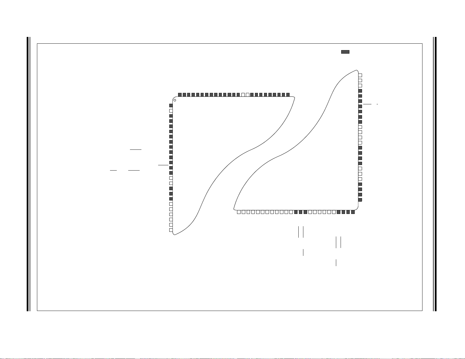
in the pinout diagrams.
© 2009-2011 Microchip Technology Inc. DS61156G-page 31

PIC32MX5XX/6XX/7XX
TABLE 1-1: PINOUT I/O DESCRIPTIONS
Pin Number
Pin Name
AN0 16 25 K2 I Analog Analog input channels.
AN1 15 24 K1 I Analog
AN2 14 23 J2 I Analog
AN3 13 22 J1 I Analog
AN4 12 21 H2 I Analog
AN5 11 20 H1 I Analog
AN6 17 26 L1 I Analog
AN7 18 27 J3 I Analog
AN8 21 32 K4 I Analog
AN9 22 33 L4 I Analog
AN10 23 34 L5 I Analog
AN11 24 35 J5 I Analog
AN12 27 41 J7 I Analog
AN13 28 42 L7 I Analog
AN14 29 43 K7 I Analog
AN15 30 44 L8 I Analog
CLKI 39 63 F9 I ST/CMOS External clock source input. Always associated
CLKO 40 64 F11 O — Oscillator crystal output. Connects to crystal or
OSC1 39 63 F9 I ST/CMOS Oscillator crystal input. ST buffer when
OSC2 40 64 F11 I/O — Oscillator crystal output. Connects to crystal or
SOSCI 47 73 C10 I ST/CMOS 32.768 kHz low-power oscillator crystal input;
SOSCO 48 74 B11 O — 32.768 kHz low-power oscillator crystal output.
Legend: CMOS = CMOS compatible input or output Analog = Analog input P = Power
Note 1: Pin numbers are provided for reference only. See the “Pin Diagrams” section for device pin availability.
2: See Section 24.0 “Ethernet Controller” for more information.
64-Pin
QFN/TQFP
ST = Schmitt Trigger input with CMOS levels O = Output I = Input
TTL = TTL input buffer
100-Pin
TQFP
(1)
121-Pin
XBGA
Pin
Type
Buffer
Type
Description
with OSC1 pin function.
resonator in Crystal Oscillator mode. Optionally
functions as CLKO in RC and EC modes.
Always associated with OSC2 pin function.
configured in RC mode; CMOS otherwise.
resonator in Crystal Oscillator mode. Optionally
functions as CLKO in RC and EC modes.
CMOS otherwise.
DS61156G-page 32 © 2009-2011 Microchip Technology Inc.

PIC32MX5XX/6XX/7XX
TABLE 1-1: PINOUT I/O DESCRIPTIONS (CONTINUED)
Pin Number
Pin Name
CN0 48 74 B11 I ST Change notification inputs.
CN1 47 73 C10 I ST
CN2 16 25 K2 I ST
CN3 15 24 K1 I ST
CN4 14 23 J2 I ST
CN5 13 22 J1 I ST
CN6 12 21 H2 I ST
CN7 11 20 H1 I ST
CN8 4 10 E3 I ST
CN9 5 11 F4 I ST
CN10 6 12 F2 I ST
CN11 8 14 F3 I ST
CN12 30 44 L8 I ST
CN13 52 81 C8 I ST
CN14 53 82 B8 I ST
CN15 54 83 D7 I ST
CN16 55 84 C7 I ST
CN17 31 49 L10 I ST
CN18 32 50 L11 I ST
CN19 — 80 D8 I ST
CN20 — 47 L9 I ST
CN21 — 48 K9 I ST
IC1 42 68 E9 I ST Capture Inputs 1-5
IC2 43 69 E10 I ST
IC3 44 70 D11 I ST
IC4 45 71 C11 I ST
IC5 52 79 A9 I ST
OCFA 17 26 L1 I ST Output Compare Fault A Input
OC1 46 72 D9 O — Output Compare Output 1
OC2 49 76 A11 O — Output Compare Output 2
OC3 50 77 A10 O — Output Compare Output 3
OC4 51 78 B9 O — Output Compare Output 4
OC5 52 81 C8 O — Output Compare Output 5
OCFB 30 44 L8 I ST Output Compare Fault B Input
INT0 46 72 D9 I ST External Interrupt 0
INT1 42 18 G1 I ST External Interrupt 1
INT2 43 19 G2 I ST External Interrupt 2
INT3 44 66 E11 I ST External Interrupt 3
INT4 45 67 E8 I ST External Interrupt 4
Legend: CMOS = CMOS compatible input or output Analog = Analog input P = Power
Note 1: Pin numbers are provided for reference only. See the “Pin Diagrams” section for device pin availability.
2: See Section 24.0 “Ethernet Controller” for more information.
64-Pin
QFN/TQFP
ST = Schmitt Trigger input with CMOS levels O = Output I = Input
TTL = TTL input buffer
100-Pin
TQFP
(1)
121-Pin
XBGA
Pin
Type
Buffer
Type
Description
Can be software programmed for internal weak
pull-ups on all inputs.
© 2009-2011 Microchip Technology Inc. DS61156G-page 33
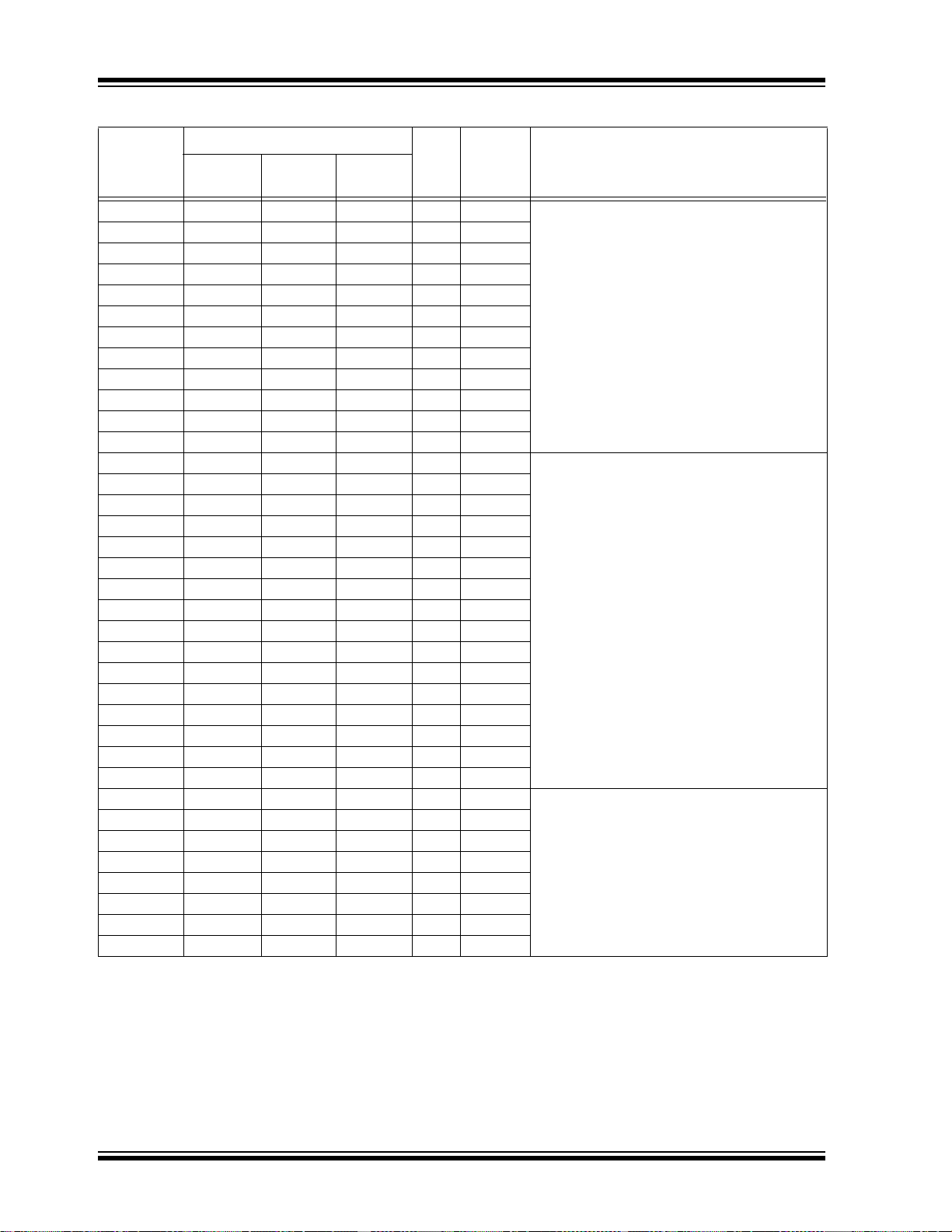
PIC32MX5XX/6XX/7XX
TABLE 1-1: PINOUT I/O DESCRIPTIONS (CONTINUED)
Pin Number
Pin Name
RA0 — 17 G3 I/O ST PORTA is a bidirectional I/O port
RA1 — 38 J6 I/O ST
RA2 — 58 H11 I/O ST
RA3 — 59 G10 I/O ST
RA4 — 60 G11 I/O ST
RA5 — 61 G9 I/O ST
RA6 — 91 C5 I/O ST
RA7 — 92 B5 I/O ST
RA9 — 28 L2 I/O ST
RA10 — 29 K3 I/O ST
RA14 — 66 E11 I/O ST
RA15 — 67 E8 I/O ST
RB0 16 25 K2 I/O ST PORTB is a bidirectional I/O port
RB1 15 24 K1 I/O ST
RB2 14 23 J2 I/O ST
RB3 13 22 J1 I/O ST
RB4 12 21 H2 I/O ST
RB5 11 20 H1 I/O ST
RB6 17 26 L1 I/O ST
RB7 18 27 J3 I/O ST
RB8 21 32 K4 I/O ST
RB9 22 33 L4 I/O ST
RB10 23 34 L5 I/O ST
RB11 24 35 J5 I/O ST
RB12 27 41 J7 I/O ST
RB13 28 42 L7 I/O ST
RB14 29 43 K7 I/O ST
RB15 30 44 L8 I/O ST
RC1 — 6 D1 I/O ST PORTC is a bidirectional I/O port
RC2 — 7 E4 I/O ST
RC3 — 8 E2 I/O ST
RC4 — 9 E1 I/O ST
RC12 39 63 F9 I/O ST
RC13 47 73 C10 I/O ST
RC14 48 74 B11 I/O ST
RC15 40 64 F11 I/O ST
Legend: CMOS = CMOS compatible input or output Analog = Analog input P = Power
Note 1: Pin numbers are provided for reference only. See the “Pin Diagrams” section for device pin availability.
2: See Section 24.0 “Ethernet Controller” for more information.
64-Pin
QFN/TQFP
ST = Schmitt Trigger input with CMOS levels O = Output I = Input
TTL = TTL input buffer
100-Pin
TQFP
(1)
121-Pin
XBGA
Pin
Type
Buffer
Type
Description
DS61156G-page 34 © 2009-2011 Microchip Technology Inc.

PIC32MX5XX/6XX/7XX
TABLE 1-1: PINOUT I/O DESCRIPTIONS (CONTINUED)
Pin Number
Pin Name
RD0 46 72 D9 I/O ST PORTD is a bidirectional I/O port
RD1 49 76 A11 I/O ST
RD2 50 77 A10 I/O ST
RD3 51 78 B9 I/O ST
RD4 52 81 C8 I/O ST
RD5 53 82 B8 I/O ST
RD6 54 83 D7 I/O ST
RD7 55 84 C7 I/O ST
RD8 42 68 E9 I/O ST
RD9 43 69 E10 I/O ST
RD10 44 70 D11 I/O ST
RD11 45 71 C11 I/O ST
RD12 — 79 A9 I/O ST
RD13 — 80 D8 I/O ST
RD14 — 47 L9 I/O ST
RD15 — 48 K9 I/O ST
RE0 60 93 A4 I/O ST PORTE is a bidirectional I/O port
RE1 61 94 B4 I/O ST
RE2 62 98 B3 I/O ST
RE3 63 99 A2 I/O ST
RE4 64 100 A1 I/O ST
RE5 1 3 D3 I/O ST
RE6 2 4 C1 I/O ST
RE7 3 5 D2 I/O ST
RE8 — 18 G1 I/O ST
RE9 — 19 G2 I/O ST
RF0 58 87 B6 I/O ST PORTF is a bidirectional I/O port
RF1 59 88 A6 I/O ST
RF2 — 52 K11 I/O ST
RF3 33 51 K10 I/O ST
RF4 31 49 L10 I/O ST
RF5 32 50 L11 I/O ST
RF8 — 53 J10 I/O ST
RF12 — 40 K6 I/O ST
RF13 — 39 L6 I/O ST
Legend: CMOS = CMOS compatible input or output Analog = Analog input P = Power
Note 1: Pin numbers are provided for reference only. See the “Pin Diagrams” section for device pin availability.
2: See Section 24.0 “Ethernet Controller” for more information.
64-Pin
QFN/TQFP
ST = Schmitt Trigger input with CMOS levels O = Output I = Input
TTL = TTL input buffer
100-Pin
TQFP
(1)
121-Pin
XBGA
Pin
Type
Buffer
Type
Description
© 2009-2011 Microchip Technology Inc. DS61156G-page 35
PIC32MX5XX/6XX/7XX
TABLE 1-1: PINOUT I/O DESCRIPTIONS (CONTINUED)
Pin Number
Pin Name
RG0 — 90 A5 I/O ST PORTG is a bidirectional I/O port
RG1 — 89 E6 I/O ST
RG6 4 10 E3 I/O ST
RG7 5 11 F4 I/O ST
RG8 6 12 F2 I/O ST
RG9 8 14 F3 I/O ST
RG12 — 96 C3 I/O ST
RG13 — 97 A3 I/O ST
RG14 — 95 C4 I/O ST
RG15 — 1 B2 I/O ST
RG2 37 57 H10 I ST PORTG input pins
RG3 36 56 J11 I ST
T1CK 48 74 B11 I ST Timer1 external clock input
T2CK — 6 D1 I ST Timer2 external clock input
T3CK — 7 E4 I ST Timer3 external clock input
T4CK — 8 E2 I ST Timer4 external clock input
T5CK — 9 E1 I ST Timer5 external clock input
U1CTS
U1RTS
U1RX
U1TX
U3CTS
U3RTS
U3RX
U3TX
U2CTS 21 40 K6 I ST UART2 clear to send
U2RTS
U2RX
U2TX
U4RX
U4TX
U6RX
U6TX
U5RX
U5TX
SCK1 — 70 D11 I/O ST Synchronous serial clock input/output for SPI1
SDI1 — 9 E1 I ST SPI1 data in
SDO1 — 72 D9 O — SPI1 data out
Legend: CMOS = CMOS compatible input or output Analog = Analog input P = Power
Note 1: Pin numbers are provided for reference only. See the “Pin Diagrams” section for device pin availability.
2: See Section 24.0 “Ethernet Controller” for more information.
64-Pin
QFN/TQFP
43 47 L9 I ST UART1 clear to send
49 48 K9 O — UART1 ready to send
50 52 K11
51 53 J10
8 14 F3 I ST UART3 clear to send
4 10 E3 O — UART3 ready to send
511F4
612F2
29 39 L6 O — UART2 ready to send
31 49 L10
32 50 L11
43 47 L9
49 48 K9
814F3
410E3
21 40 K6
29 39 L6
ST = Schmitt Trigger input with CMOS levels O = Output I = Input
TTL = TTL input buffer
100-Pin
TQFP
(1)
121-Pin
XBGA
Pin
Type
Buffer
Type
I ST UART1 receive
O — UART1 transmit
I ST UART3 receive
O — UART3 transmit
I ST UART2 receive
O — UART2 transmit
I ST UART4 receive
O — UART4 transmit
I ST UART6 receive
O — UART6 transmit
I ST UART5 receive
O — UART5 transmit
Description
DS61156G-page 36 © 2009-2011 Microchip Technology Inc.

PIC32MX5XX/6XX/7XX
TABLE 1-1: PINOUT I/O DESCRIPTIONS (CONTINUED)
Pin Number
Pin Name
SS1 — 69 E10 I/O ST SPI1 slave synchronization or frame pulse I/O
SCK3 49 48 K9 I/O ST Synchronous serial clock input/output for SPI3
SDI3 50 52 K11 I ST SPI3 data in
SDO3 51 53 J10 O — SPI3 data out
SS3
SCK2 4 10 E3 I/O ST Synchronous serial clock input/output for SPI2
SDI2 5 11 F4 I ST SPI2 data in
SDO2 6 12 F2 O — SPI2 data out
SS2
SCK4 29 39 L6 I/O ST Synchronous serial clock input/output for SPI4
SDI4 31 49 L10 I ST SPI4 data in
SDO4 32 50 L11 O — SPI4 data out
SS4
SCL1 44 66 E11 I/O ST Synchronous serial clock input/output for I2C1
SDA1 43 67 E8 I/O ST Synchronous serial data input/output for I2C1
SCL3 51 53 J10 I/O ST Synchronous serial clock input/output for I2C3
SDA3 50 52 K11 I/O ST Synchronous serial data input/output for I2C3
SCL2 — 58 H11 I/O ST Synchronous serial clock input/output for I2C2
SDA2 — 59 G10 I/O ST Synchronous serial data input/output for I2C2
SCL4 6 12 F2 I/O ST Synchronous serial clock input/output for I2C4
SDA4 5 11 F4 I/O ST Synchronous serial data input/output for I2C4
SCL5 32 50 L11 I/O ST Synchronous serial clock input/output for I2C5
SDA5 31 49 L10 I/O ST Synchronous serial data input/output for I2C5
TMS 23 17 G3 I ST JTAG Test mode select pin
TCK 27 38 J6 I ST JTAG test clock input pin
TDI 28 60 G11 I ST JTAG test data input pin
TDO 24 61 G9 O — JTAG test data output pin
RTCC 42 68 E9 O — Real-Time Clock alarm output
CV
REF- 15 28 L2 I Analog Comparator Voltage Reference (low)
CVREF+ 16 29 K3 I Analog Comparator Voltage Reference (high)
CV
REFOUT 23 34 L5 O Analog Comparator Voltage Reference output
C1IN- 12 21 H2 I Analog Comparator 1 negative input
C1IN+ 11 20 H1 I Analog Comparator 1 positive input
C1OUT 21 32 K4 O — Comparator 1 output
C2IN- 14 23 J2 I Analog Comparator 2 negative input
C2IN+ 13 22 J1 I Analog Comparator 2 positive input
C2OUT 22 33 L4 O — Comparator 2 output
Legend: CMOS = CMOS compatible input or output Analog = Analog input P = Power
Note 1: Pin numbers are provided for reference only. See the “Pin Diagrams” section for device pin availability.
2: See Section 24.0 “Ethernet Controller” for more information.
64-Pin
QFN/TQFP
43 47 L9 I/O ST SPI3 slave synchronization or frame pulse I/O
8 14 F3 I/O ST SPI2 slave synchronization or frame pulse I/O
21 40 K6 I/O ST SPI4 slave synchronization or frame pulse I/O
ST = Schmitt Trigger input with CMOS levels O = Output I = Input
TTL = TTL input buffer
100-Pin
TQFP
(1)
121-Pin
XBGA
Pin
Type
Buffer
Type
Description
© 2009-2011 Microchip Technology Inc. DS61156G-page 37

PIC32MX5XX/6XX/7XX
TABLE 1-1: PINOUT I/O DESCRIPTIONS (CONTINUED)
Pin Number
Pin Name
PMA0 30 44 L8 I/O TTL/ST Parallel Master Port Address bit 0 input
PMA1 29 43 K7 I/O TTL/ST Parallel Master Port Address bit 1 input
PMA2 8 14 F3 O — Parallel Master Port address (Demultiplexed
PMA3 6 12 F2 O —
PMA4 5 11 F4 O —
PMA5 4 10 E3 O —
PMA6 16 29 K3 O —
PMA7 22 28 L2 O —
PMA8 32 50 L11 O —
PMA9 31 49 L10 O —
PMA10 28 42 L7 O —
PMA11 27 41 J7 O —
PMA12 24 35 J5 O —
PMA13 23 34 L5 O —
PMA14 45 71 C11 O —
PMA15 44 70 D11 O —
PMCS1 45 71 C11 O — Parallel Master Port Chip Select 1 strobe
PMCS2 44 70 D11 O — Parallel Master Port Chip Select 2 strobe
PMD0 60 93 A4 I/O TTL/ST Parallel Master Port data (Demultiplexed
PMD1 61 94 B4 I/O TTL/ST
PMD2 62 98 B3 I/O TTL/ST
PMD3 63 99 A2 I/O TTL/ST
PMD4 64 100 A1 I/O TTL/ST
PMD5 1 3 D3 I/O TTL/ST
PMD6 2 4 C1 I/O TTL/ST
PMD7 3 5 D2 I/O TTL/ST
PMD8 — 90 A5 I/O TTL/ST
PMD9 — 89 E6 I/O TTL/ST
PMD10 — 88 A6 I/O TTL/ST
PMD11 — 87 B6 I/O TTL/ST
PMD12 — 79 A9 I/O TTL/ST
PMD13 — 80 D8 I/O TTL/ST
PMD14 — 83 D7 I/O TTL/ST
PMD15 — 84 C7 I/O TTL/ST
Legend: CMOS = CMOS compatible input or output Analog = Analog input P = Power
Note 1: Pin numbers are provided for reference only. See the “Pin Diagrams” section for device pin availability.
2: See Section 24.0 “Ethernet Controller” for more information.
64-Pin
QFN/TQFP
ST = Schmitt Trigger input with CMOS levels O = Output I = Input
TTL = TTL input buffer
100-Pin
TQFP
(1)
121-Pin
XBGA
Pin
Type
Buffer
Type
Description
(Buffered Slave modes) and output (Master
modes)
(Buffered Slave modes) and output (Master
modes)
Master modes)
Master mode) or address/data (Multiplexed
Master modes)
DS61156G-page 38 © 2009-2011 Microchip Technology Inc.

PIC32MX5XX/6XX/7XX
TABLE 1-1: PINOUT I/O DESCRIPTIONS (CONTINUED)
Pin Number
Pin Name
64-Pin
QFN/TQFP
100-Pin
TQFP
PMALL 30 44 L8 O — Parallel Master Port address latch enable
PMALH 29 43 K7 O — Parallel Master Port address latch enable
PMRD 53 82 B8 O — Parallel Master Port read strobe
PMWR 52 81 C8 O — Parallel Master Port write strobe
BUS 34 54 H8 I Analog USB bus power monitor
V
VUSB 35 55 H9 P — USB internal transceiver supply. If the USB
VBUSON 11 20 H1 O — USB Host and OTG bus power control output
D+ 37 57 H10 I/O Analog USB D+
D- 36 56 J11 I/O Analog USB D-
USBID 33 51 K10 I ST USB OTG ID detect
C1RX 58 87 B6 I ST CAN1 bus receive pin
C1TX 59 88 A6 O — CAN1 bus transmit pin
AC1RX 32 40 K6 I ST Alternate CAN1 bus receive pin
AC1TX 31 39 L6 O — Alternate CAN1 bus transmit pin
C2RX 29 90 A5 I ST CAN2 bus receive pin
C2TX 21 89 E6 O — CAN2 bus transmit pin
AC2RX — 8 E2 1 ST Alternate CAN2 bus receive pin
AC2TX — 7 E4 O — Alternate CAN2 bus transmit pin
ERXD0 61 41 J7 I ST Ethernet Receive Data 0
ERXD1 60 42 L7 I ST Ethernet Receive Data 1
ERXD2 59 43 K7 I ST Ethernet Receive Data 2
ERXD3 58 44 L8 I ST Ethernet Receive Data 3
ERXERR 64 35 J5 I ST Ethernet receive error input
ERXDV 62 12 F2 I ST Ethernet receive data valid
ECRSDV 62 12 F2 I ST Ethernet carrier sense data valid
ERXCLK 63 14 F3 I ST Ethernet receive clock
EREFCLK 63 14 F3 I ST Ethernet reference clock
ETXD0 2 88 A6 O — Ethernet Transmit Data 0
ETXD1 3 87 B6 O — Ethernet Transmit Data 1
ETXD2 43 79 A9 O — Ethernet Transmit Data 2
ETXD3 42 80 D8 O — Ethernet Transmit Data 3
ETXERR 54 89 E6 O — Ethernet transmit error
ETXEN 1 83 D7 O — Ethernet transmit enable
ETXCLK 55 84 C7 I ST Ethernet transmit clock
ECOL 44 10 E3 I ST Ethernet collision detect
ECRS 45 11 F4 I ST Ethernet carrier sense
Legend: CMOS = CMOS compatible input or output Analog = Analog input P = Power
ST = Schmitt Trigger input with CMOS levels O = Output I = Input
TTL = TTL input buffer
Note 1: Pin numbers are provided for reference only. See the “Pin Diagrams” section for device pin availability.
2: See Section 24.0 “Ethernet Controller” for more information.
(1)
121-Pin
XBGA
Pin
Type
Buffer
Type
Description
low byte (Multiplexed Master modes)
high byte (Multiplexed Master modes)
module is not used, this pin must be connected
DD.
to V
(2)
(2)
(2)
(2)
(2)
(2)
(2)
(2)
(2)
(2)
(2)
(2)
(2)
(2)
(2)
(2)
(2)
(2)
© 2009-2011 Microchip Technology Inc. DS61156G-page 39

PIC32MX5XX/6XX/7XX
TABLE 1-1: PINOUT I/O DESCRIPTIONS (CONTINUED)
Pin Number
Pin Name
64-Pin
QFN/TQFP
100-Pin
TQFP
EMDC 30 71 C11 O — Ethernet management data clock
EMDIO 49 68 E9 I/O — Ethernet management data
AERXD0 43 18 G1 I ST Alternate Ethernet Receive Data 0
AERXD1 42 19 G2 I ST Alternate Ethernet Receive Data 1
AERXD2 — 28 L2 I ST Alternate Ethernet Receive Data 2
AERXD3 — 29 K3 I ST Alternate Ethernet Receive Data 3
AERXERR 55 1 B2 I ST Alternate Ethernet receive error input
AERXDV — 12 F2 I ST Alternate Ethernet receive data valid
AECRSDV 44 12 F2 I ST Alternate Ethernet carrier sense data valid
AERXCLK — 14 F3 I ST Alternate Ethernet receive clock
AEREFCLK 45 14 F3 I ST Alternate Ethernet reference clock
AETXD0 59 47 L9 O — Alternate Ethernet Transmit Data 0
AETXD1 58 48 K9 O — Alternate Ethernet Transmit Data 1
AETXD2 — 44 L8 O — Alternate Ethernet Transmit Data 2
AETXD3 — 43 K7 O — Alternate Ethernet Transmit Data 3
AETXERR — 35 J5 O — Alternate Ethernet transmit error
AETXEN 54 67 E8 O — Alternate Ethernet transmit enable
AETXCLK — 66 E11 I ST Alternate Ethernet transmit clock
AECOL — 42 L7 I ST Alternate Ethernet collision detect
AECRS — 41 J7 I ST Alternate Ethernet carrier sense
AEMDC 30 71 C11 O — Alternate Ethernet Management Data clock
AEMDIO 49 68 E9 I/O — Alternate Ethernet Management Data
TRCLK — 91 C5 O — Trace clock
TRD0 — 97 A3 O — Trace Data bits 0-3
TRD1 — 96 C3 O —
TRD2 — 95 C4 O —
TRD3 — 92 B5 O —
PGED1 16 25 K2 I/O ST Data I/O pin for Programming/Debugging
PGEC1 15 24 K1 I ST Clock input pin for Programming/Debugging
PGED2 18 27 J3 I/O ST Data I/O pin for Programming/Debugging
PGEC2 17 26 L1 I ST Clock input pin for Programming/Debugging
MCLR
7 13 F1 I/P ST Master Clear (Reset) input. This pin is an
Legend: CMOS = CMOS compatible input or output Analog = Analog input P = Power
ST = Schmitt Trigger input with CMOS levels O = Output I = Input
TTL = TTL input buffer
Note 1: Pin numbers are provided for reference only. See the “Pin Diagrams” section for device pin availability.
2: See Section 24.0 “Ethernet Controller” for more information.
(1)
121-Pin
XBGA
Pin
Type
Buffer
Type
Description
(2)
(2)
(2)
(2)
(2)
(2)
(2)
(2)
(2)
(2)
(2)
(2)
(2)
(2)
(2)
(2)
(2)
(2)
(2)
(2)
Communication Channel 1
Communication Channel 1
Communication Channel 2
Communication Channel 2
active-low Reset to the device.
(2)
(2)
DS61156G-page 40 © 2009-2011 Microchip Technology Inc.

PIC32MX5XX/6XX/7XX
TABLE 1-1: PINOUT I/O DESCRIPTIONS (CONTINUED)
Pin Number
Pin Name
AVDD 19 30 J4 P P Positive supply for analog modules. This pin
SS 20 31 L3 P P Ground reference for analog modules
AV
VDD 10, 26, 38, 572, 16, 37,
CAP/VCORE 56 85 B7 P — Capacitor for Internal Voltage Regulator
V
VSS 9, 25, 41 15, 36, 45,
REF+ 16 29 K3 I Analog Analog voltage reference (high) input
V
VREF- 15 28 L2 I Analog Analog voltage reference (low) input
Legend: CMOS = CMOS compatible input or output Analog = Analog input P = Power
Note 1: Pin numbers are provided for reference only. See the “Pin Diagrams” section for device pin availability.
2: See Section 24.0 “Ethernet Controller” for more information.
64-Pin
QFN/TQFP
ST = Schmitt Trigger input with CMOS levels O = Output I = Input
TTL = TTL input buffer
100-Pin
TQFP
46, 62, 86
65, 75
(1)
121-Pin
XBGA
A7, C2,
C9, E5,
K8, F8,
G5, H4, H6
A8, B10,
D4, D5,
E7, F5,
F10, G6,
G7, H3
Pin
Type
Buffer
Type
must be connected at all times.
P — Positive supply for peripheral logic and I/O pins
P — Ground reference for logic and I/O pins. This
pin must be connected at all times.
Description
© 2009-2011 Microchip Technology Inc. DS61156G-page 41

PIC32MX5XX/6XX/7XX
NOTES:
DS61156G-page 42 © 2009-2011 Microchip Technology Inc.

PIC32MX5XX/6XX/7XX
2.0 GUIDELINES FOR GETTING STARTED WITH 32-BIT MICROCONTROLLERS
Note 1: This data sheet summarizes the features
of the PIC32MX5XX/6XX/7XX family of
devices. It is not intended to be a
comprehensive reference source. To
complement the information in this data
sheet, refer to the related section of the
“PIC32 Family Reference Manual”, which
is available from the Microchip web site
(www.microchip.com/PIC32).
2: Some registers and associated bits
described in this section may not be
available on all devices. Refer to
Section 4.0 “Memory Organization” in
this data sheet for device-specific register
and bit information.
2.1 Basic Connection Requirements
Getting started with the PIC32MX5XX/6XX/7XX family
of 32-bit Microcontrollers (MCUs) requires attention to
a minimal set of device pin connections before proceeding with development. The following is a list of pin
names, which must always be connected:
DD and VSS pins
• All V
(see Section 2.2 “Decoupling Capacitors”)
• All AV
•V
•MCLR
• PGECx/PGEDx pins used for In-Circuit Serial
• OSC1 and OSC2 pins when external oscillator
The following pin may be required, as well:
V
for ADC module is implemented
DD and AVSS pins even if the ADC module is
not used
(see Section 2.2 “Decoupling Capacitors”)
CAP/VCORE pin
(see Section 2.3 “Capacitor on Internal Voltage
Regulator (V
(see Section 2.4 “Master Clear (MCLR) Pin”)
Programming™ (ICSP™) and debugging
purposes
(see Section 2.5 “ICSP Pins”)
source is used
(see Section 2.8 “External Oscillator Pins”)
REF+/VREF- pins used when external voltage reference
Note: The AV
CAP/VCORE)”)
pin
DD and AVSS pins must be
connected, regardless of the ADC use
and the ADC voltage reference source.
2.2 Decoupling Capacitors
The use of decoupling capacitors on power supply
pins, such as V
See Figure 2-1.
Consider the following criteria when using decoupling
capacitors:
• Value and type of capacitor: A value of 0.1 µF
(100 nF), 10-20V is recommended. The capacitor
should be a low Equivalent Series Resistance
(low-ESR) capacitor and have resonance frequency in the range of 20 MHz and higher. It is
further recommended to use ceramic capacitors.
• Placement on the printed circuit board: The
decoupling capacitors should be placed as close
to the pins as possible. It is recommended that
the capacitors be placed on the same side of
the board as the device. If space is constricted,
the capacitor can be placed on another layer on
the PCB using a via; however, ensure that the
trace length from the pin to the capacitor is
within one-quarter inch (6 mm) in length.
• Handling high frequency noise: If the board is
experiencing high frequency noise, upward of
tens of MHz, add a second ceramic-type capacitor
in parallel to the above described decoupling
capacitor. The value of the second capacitor can
be in the range of 0.01 µF to 0.001 µF. Place this
second capacitor next to the primary decoupling
capacitor. In high-speed circuit designs, consider
implementing a decade pair of capacitances as
close to the power and ground pins as possible.
For example, 0.1 µF in parallel with 0.001 µF.
• Maximizing performance: On the board layout
from the power supply circuit, run the power and
return traces to the decoupling capacitors first,
and then to the device pins. This ensures that the
decoupling capacitors are first in the power chain.
Equally important is to keep the trace length
between the capacitor and the power pins to a
minimum, thereby reducing PCB track
inductance.
DD, VSS, AVDD and AVSS is required.
© 2009-2011 Microchip Technology Inc. DS61156G-page 43

PIC32MX5XX/6XX/7XX
PIC32
VDD
VSS
VDD
VSS
VSS
VDD
AVDD
AVSS
VDD
VSS
C
R
V
DD
MCLR
0.1 µF
Ceramic
VCAP/VCORE
10 Ω
R1
CBP
0.1 µF
Ceramic
C
BP
0.1 µF
Ceramic
C
BP
0.1 µF
Ceramic
C
BP
0.1 µF
Ceramic
C
BP
CEFC
Note 1: R ≤ 10 kΩ is recommended. A suggested start-
ing value is 10 kΩ. Ensure that the MCLR
pin
V
IH and VIL specifications are met.
2: R1 ≤ 470Ω will limit any current flowing into
MCLR
from the external capacitor C, in the
event of MCLR
pin breakdown, due to
Electrostatic Discharge (ESD) or Electrical
Overstress (EOS). Ensure that the MCLR
pin
V
IH and VIL specifications are met.
3: The capacitor can be sized to prevent uninten-
tional Resets from brief glitches or to extend
the device Reset period during the POR.
C
R1
R
V
DD
MCLR
PIC32
JP
FIGURE 2-1: RECOMMENDED
MINIMUM CONNECTION
2.2.1 BULK CAPACITORS
The use of a bulk capacitor is recommended to improve
power supply stability. Typical values range from 4.7 µF
to 47 µF. This capacitor should be located as close to
the device as possible.
2.4 Master Clear (MCLR) Pin
The MCLR pin provides two specific device
functions:
• Device Reset
• Device Programming and Debugging
Pulling The MCLR
Figure 2-2 illustrates a typical MCLR
device programming and debugging, the resistance
and capacitance that can be added to the pin must
be considered. Device programmers and debuggers
drive the MCLR
levels (V
IH and VIL) and fast signal transitions must
not be adversely affected. Therefore, specific values
of R and C will need to be adjusted based on the
application and PCB requirements.
For example, as illustrated in Figure 2-2, it is
recommended that the capacitor C, be isolated from
the MCLR
pin during programming and debugging
operations.
Place the components illustrated in Figure 2-2 within
one-quarter inch (6 mm) from the MCLR
FIGURE 2-2: EXAMPLE OF MCLR PIN
pin low generates a device Reset.
circuit. During
pin. Consequently, specific voltage
pin.
CONNECTIONS
2.3 Capacitor on Internal Voltage
CAP/VCORE)
CAP/VCORE pin must not
Regulator (V
2.3.1 INTERNAL REGULATOR MODE
A low-ESR (1 ohm) capacitor is required on the
VCAP/VCORE pin, which is used to stabilize the internal
voltage regulator output. The V
be connected to VDD, and must have a CEFC capacitor, with at least a 6V rating, connected to ground. The
type can be ceramic or tantalum. Refer to Section 31.0
“Electrical Characteristics” for additional information
EFC specifications.
on C
DS61156G-page 44 © 2009-2011 Microchip Technology Inc.

PIC32MX5XX/6XX/7XX
2.5 ICSP Pins
The PGECx and PGEDx pins are used for In-Circuit
Serial Programming™ (ICSP™) and debugging purposes. It is recommended to keep the trace length
between the ICSP connector and the ICSP pins on the
device as short as possible. If the ICSP connector is
expected to experience an ESD event, a series resistor
is recommended, with the value in the range of a few
tens of Ohms, not to exceed 100 Ohms.
Pull-up resistors, series diodes and capacitors on the
PGECx and PGEDx pins are not recommended as they
will interfere with the programmer/debugger communications to the device. If such discrete components are
an application requirement, they should be removed
from the circuit during programming and debugging.
Alternatively, refer to the AC/DC characteristics and
timing requirements information in the respective
device Flash programming specification for information
on capacitive loading limits and pin input voltage high
IH) and input low (VIL) requirements.
(V
Ensure that the “Communication Channel Select” (i.e.,
PGECx/PGEDx pins) programmed into the device
matches the physical connections for the ICSP to
®
MPLAB
ICE™.
For more information on ICD 2, ICD 3 and REAL ICE
connection requirements, refer to the following
documents that are available on the Microchip web
site.
• “MPLAB
• “Using MPLAB
• “MPLAB® ICD 2 Design Advisory” DS51566
• “Using MPLAB
• “MPLAB
• “MPLAB
• “Using MPLAB
ICD 2, MPLAB® ICD 3 or MPLAB® REAL
®
ICD 2 In-Circuit Debugger User’s
Guide” DS51331
Guide” DS51616
DS51749
®
ICD 2” (poster) DS51265
®
®
®
ICD 3” (poster) DS51765
ICD 3 Design Advisory” DS51764
REAL ICE™ In-Circuit Emulator User’s
®
REAL ICE™ Emulator” (poster)
2.6 JTAG
The TMS, TDO, TDI and TCK pins are used for testing
and debugging according to the Joint Test Action
Group (JTAG) standard. It is recommended to keep the
trace length between the JTAG connector and the
JTAG pins on the device as short as possible. If the
JTAG connector is expected to experience an ESD
event, a series resistor is recommended, with the value
in the range of a few tens of Ohms, not to exceed 100
Ohms.
Pull-up resistors, series diodes and capacitors on the
TMS, TDO, TDI and TCK pins are not recommended
as they will interfere with the programmer/debugger
communications to the device. If such discrete components are an application requirement, they should be
removed from the circuit during programming and
debugging. Alternatively, refer to the AC/DC characteristics and timing requirements information in the
respective device Flash programming specification for
information on capacitive loading limits and pin input
voltage high (V
IH) and input low (VIL) requirements.
2.7 Trace
The trace pins can be connected to a hardware-traceenabled programmer to provide a compress real time
instruction trace. When used for trace the TRD3,
TRD2, TRD1, TRD0 and TRCLK pins should be
dedicated for this use. The trace hardware requires
a22Ω series resistor between the trace pins and the
trace connector.
© 2009-2011 Microchip Technology Inc. DS61156G-page 45

PIC32MX5XX/6XX/7XX
Main Oscillator
Guard Ring
Guard Trace
Secondary
Oscillator
2.8 External Oscillator Pins
Many MCUs have options for at least two oscillators: a
high-frequency primary oscillator and a low-frequency
secondary oscillator. Refer to Section 8.0 “Oscillator
Configuration” for details.
The oscillator circuit should be placed on the same side
of the board as the device. Also, place the oscillator circuit close to the respective oscillator pins, not exceeding one-half inch (12 mm) distance between them. The
load capacitors should be placed next to the oscillator
itself, on the same side of the board. Use a grounded
copper pour around the oscillator circuit to isolate them
from surrounding circuits. The grounded copper pour
should be routed directly to the MCU ground. Do not
run any signal traces or power traces inside the ground
pour. Also, if using a two-sided board, avoid any traces
on the other side of the board where the crystal is
placed. A suggested layout is illustrated in Figure 2-3.
FIGURE 2-3: SUGGESTED OSCILLATOR
CIRCUIT PLACEMENT
2.9 Configuration of Analog and Digital Pins During ICSP Operations
If MPLAB ICD 2, ICD 3 or REAL ICE is selected as
a debugger, it automatically initializes all of the
Analog-to-Digital input pins (ANx) as “digital” pins by
setting all bits in the ADPCFG register.
The bits in this register that correspond to the Analogto-Digital pins that are initialized by MPLAB ICD 2, ICD
3 or REAL ICE, must not be cleared by the user
application firmware; otherwise, communication errors
will result between the debugger and the device.
If your application needs to use certain ADC pins as
analog input pins during the debug session, the user
application must clear the corresponding bits in the
ADPCFG register during initialization of the ADC
module.
When MPLAB ICD 2, ICD 3 or REAL ICE is used as a
programmer, the user application firmware must correctly configure the ADPCFG register. Automatic initialization of this register is only done during debugger
operation. Failure to correctly configure the register(s)
will result in all ADC pins being recognized as analog
input pins, resulting in the port value being read as a
logic ‘0’, which may affect user application functionality.
2.10 Unused I/Os
Unused I/O pins should not be allowed to float as
inputs. They can be configured as outputs and driven
to a logic-low state.
Alternatively, inputs can be reserved by connecting the
pin to V
the pin as an input.
SS through a 1k to 10k resistor and configuring
DS61156G-page 46 © 2009-2011 Microchip Technology Inc.

PIC32MX5XX/6XX/7XX
2.11 Referenced Sources
This device data sheet is based on the following
individual chapters of the “PIC32 Family Reference
Manual”. These documents should be considered as
the general reference for the operation of a particular
module or device feature.
Note 1: To access the documents listed below,
browse to the documentation section of
the PIC32MX795F512L product page on
the Microchip web site
(www.microchip.com) or select a family
reference manual section from the
following list.
In addition to parameters, features, and
other documentation, the resulting page
provides links to the related family
reference manual sections.
• Section 1. “Introduction” (DS61127)
• Section 2. “CPU” (DS 6 111 3 )
• Section 4. “Prefetch Cache” (DS61119)
• Section 3. “Memory Organization” (DS61115)
• Section 5. “Flash Program Memory” (DS61121)
• Section 6. “Oscillator Configuration” (DS61112)
• Section 7. “Resets” (D S 6 111 8 )
• Section 8. “Interrupt Controller” (DS61108)
• Section 9. “Watchdog Timer and Power-up Timer (DS61114)
• Section 10. “Power-Saving Features” (DS61130)
• Section 12. “I/O Ports” (DS61120)
• Section 13. “Parallel Master Port (PMP)” (DS61128)
• Section 14. “Timers” (DS61105)
• Section 15. “Input Capture” (DS61122)
• Section 16. “Output Capture” (DS61111)
• Section 17. “10-bit Analog-to-Digital Converter (ADC)” (DS61104)
• Section 19. “Comparator” (D S 6 1110)
• Section 20. “Comparator Voltage Reference (CV
• Section 21. “Universal Asynchronous Receiver Transmitter (UART)” (DS61107)
• Section 23. “Serial Peripheral Interface (SPI)” (DS61106)
• Section 24. “Inter-Integrated Circuit (I2C™)” (DS61116)
• Section 27. “USB On-The-Go (OTG)” (DS61126)
• Section 29. “Real-Time Clock and Calendar (RTCC)” (DS61125)
• Section 31. “Direct Memory Access (DMA) Controller” (DS61117)
• Section 32. “Configuration” (DS61124)
• Section 33. “Programming and Diagnostics” (DS61129)
• Section 34. “Controller Area Network (CAN)” (DS61154)
• Section 35. “Ethernet Controller” (DS61155)
REF)” (DS61109)
© 2009-2011 Microchip Technology Inc. DS61156G-page 47

PIC32MX5XX/6XX/7XX
NOTES:
DS61156G-page 48 © 2009-2011 Microchip Technology Inc.
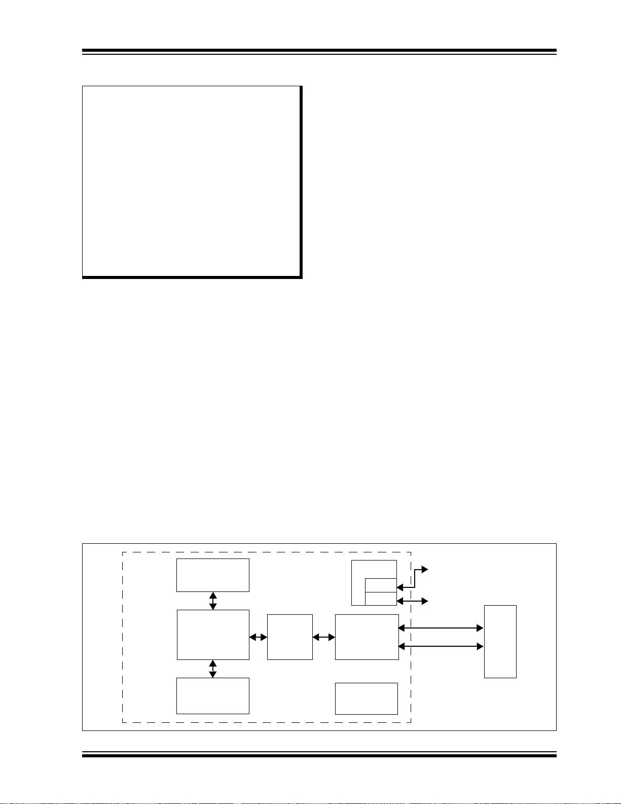
PIC32MX5XX/6XX/7XX
Dual Bus I/F
System
Coprocessor
MDU
FMT
TAP
EJTAG
Power
Management
Off-Chip
Debug I/F
Execution
Core
(RF/ALU/Shift)
Bus Matrix
Trace
Trace I/F
Bus Interface
CPU
3.0 CPU
Note 1: This data sheet summarizes the features
of the PIC32MX5XX/6XX/7XX family of
devices. It is not intended to be a
comprehensive reference source. To
complement the information in this data
sheet, refer to Section 2. “CPU”
(DS61113) in the “PIC32 Family
Reference Manual”, which is available
from the Microchip web site (www.micro-
chip.com/PIC32). Resources for the
MIPS32
available at http://www.mips.com.
2: Some registers and associated bits
described in this section may not be
available on all devices. Refer to
Section 4.0 “Memory Organization” in
this data sheet for device-specific register
and bit information.
The MIPS32® M4K® Processor core is the heart of the
PIC32MX5XX/6XX/7XX family processor. The CPU
fetches instructions, decodes each instruction, fetches
source operands, executes each instruction and writes
the results of instruction execution to the proper
destinations.
3.1 Features
• 5-stage pipeline
• 32-bit address and data paths
• MIPS32 Enhanced Architecture (Release 2)
- Multiply-accumulate and multiply-subtract
instructions
- Targeted multiply instruction
- Zero/One detect instructions
- WAIT instruction
- Conditional move instructions (MOVN, MOVZ)
- Vectored interrupts
- Programmable exception vector base
®
M4K® Processor Core are
- Atomic interrupt enable/disable
- GPR shadow registers to minimize latency
for interrupt handlers
- Bit field manipulation instructions
• MIPS16e
- 16-bit encoding of 32-bit instructions to
- Special PC-relative instructions for efficient
- SAVE and RESTORE macro instructions for
- Improved support for handling 8 and 16-bit
• Simple Fixed Mapping Translation (FMT)
mechanism
• Simple dual bus interface
- Independent 32-bit address and data busses
- Transactions can be aborted to improve
• Autonomous multiply/divide unit
- Maximum issue rate of one 32x16 multiply
- Maximum issue rate of one 32x32 multiply
- Early-in iterative divide. Minimum 11 and
• Power control
- Minimum frequency: 0 MHz
- Low-Power mode (triggered by WAIT
- Extensive use of local gated clocks
• EJTAG debug and instruction trace
- Support for single stepping
- Virtual instruction and data address/value
- Breakpoints
- PC tracing with trace compression
®
code compression
improve code density
loading of addresses and constants
setting up and tearing down stack frames
within subroutines
data types
interrupt latency
per clock
every other clock
maximum 33 clock latency (dividend (rs) sign
extension-dependent)
instruction)
FIGURE 3-1: MIPS® M4K® PROCESSOR CORE BLOCK DIAGRAM
© 2009-2011 Microchip Technology Inc. DS61156G-page 49

PIC32MX5XX/6XX/7XX
3.2 Architecture Overview
The MIPS® M4K® processor core contains several
logic blocks working together in parallel, providing an
efficient high-performance computing engine. The
following blocks are included with the core:
• Execution Unit
• Multiply/Divide Unit (MDU)
• System Control Coprocessor (CP0)
• Fixed Mapping Translation (FMT)
• Dual Internal Bus interfaces
• Power Management
• MIPS16e Support
• Enhanced JTAG (EJTAG) Controller
3.2.1 EXECUTION UNIT
The MIPS M4K processor core execution unit implements a load/store architecture with single-cycle ALU
operations (logical, shift, add, subtract) and an autonomous multiply/divide unit. The core contains thirty-two
32-bit General Purpose Registers (GPRs) used for
integer operations and address calculation. One additional register file shadow set (containing thirty-two registers) is added to minimize context switching overhead
during interrupt/exception processing. The register file
consists of two read ports and one write port and is fully
bypassed to minimize operation latency in the pipeline.
The execution unit includes:
• 32-bit adder used for calculating the data address
• Address unit for calculating the next instruction
address
• Logic for branch determination and branch target
address calculation
• Load aligner
• Bypass multiplexers used to avoid stalls when
executing instruction streams where data
producing instructions are followed closely by
consumers of their results
• Leading Zero/One detect unit for implementing
the CLZ and CLO instructions
• Arithmetic Logic Unit (ALU) for performing bitwise
logical operations
• Shifter and store aligner
3.2.2 MULTIPLY/DIVIDE UNIT (MDU)
MIPS M4K processor core includes a Multiply/Divide
Unit (MDU) that contains a separate pipeline for multiply and divide operations. This pipeline operates in parallel with the Integer Unit (IU) pipeline and does not stall
when the IU pipeline stalls. This allows MDU operations to be partially masked by system stalls and/or
other integer unit instructions.
The high-performance MDU consists of a 32x16 booth
recoded multiplier, result/accumulation registers (HI
and LO), a divide state machine, and the necessary
multiplexers and control logic. The first number shown
(‘32’ of 32x16) represents the rs operand. The second
number (‘16’ of 32x16) represents the rt operand. The
PIC32 core only checks the value of the latter (rt)
operand to determine how many times the operation
must pass through the multiplier. The 16x16 and 32x16
operations pass through the multiplier once. A 32x32
operation passes through the multiplier twice.
The MDU supports execution of one 16x16 or 32x16
multiply operation every clock cycle; 32x32 multiply
operations can be issued every other clock cycle.
Appropriate interlocks are implemented to stall the
issuance of back-to-back 32x32 multiply operations.
The multiply operand size is automatically determined
by logic built into the MDU.
Divide operations are implemented with a simple 1 bit
per clock iterative algorithm. An early-in detection
checks the sign extension of the dividend (rs) operand.
If rs is 8 bits wide, 23 iterations are skipped. For a 16 bit
wide rs, 15 iterations are skipped and for a 24 bit wide rs,
7 iterations are skipped. Any attempt to issue a
subsequent MDU instruction while a divide is still active
causes an IU pipeline stall until the divide operation is
completed.
Table 3-1 lists the repeat rate (peak issue rate of cycles
until the operation can be reissued) and latency (number of cycles until a result is available) for the PIC32
core multiply and divide instructions. The approximate
latency and repeat rates are listed in terms of pipeline
clocks.
DS61156G-page 50 © 2009-2011 Microchip Technology Inc.

PIC32MX5XX/6XX/7XX
TABLE 3-1: MIPS® M4K® CORE HIGH-PERFORMANCE INTEGER MULTIPLY/DIVIDE UNIT
LATENCIES AND REPEAT RATES
Opcode Operand Size (mul rt) (div rs) Latency Repeat Rate
MULT/MULTU, MADD/MADDU,
MSUB/MSUBU
MUL 16 bits 2 1
DIV/DIVU 8 bits 12 11
16 bits 1 1
32 bits 2 2
32 bits 3 2
16 bits 19 18
24 bits 26 25
32 bits 33 32
The MIPS architecture defines that the result of a
multiply or divide operation be placed in the HI and LO
registers. Using the Move-From-HI (MFHI) and MoveFrom-LO (MFLO) instructions, these values can be
transferred to the General Purpose Register file.
In addition to the HI/LO targeted operations, the
MIPS32 architecture also defines a multiply instruction,
MUL, which places the least significant results in the primary register file instead of the HI/LO register pair. By
avoiding the explicit MFLO instruction required when
using the LO register, and by supporting multiple destination registers, the throughput of multiply-intensive
operations is increased.
Two other instructions, Multiply-Add (MADD) and
Multiply-Subtract (MSUB), are used to perform the
multiply-accumulate and multiply-subtract operations.
The MADD instruction multiplies two numbers and then
adds the product to the current contents of the HI and
LO registers. Similarly, the MSUB instruction multiplies
two operands and then subtracts the product from the
HI and LO registers. The MADD and MSUB operations
are commonly used in DSP algorithms.
3.2.3 SYSTEM CONTROL
COPROCESSOR (CP0)
In the MIPS architecture, CP0 is responsible for the
virtual-to-physical address translation, the exception
control system, the processor’s diagnostics capability,
the operating modes (Kernel, User and Debug) and
whether interrupts are enabled or disabled. Configuration information, such as presence of options like
MIPS16e, is also available by accessing the CP0
registers, listed in Ta bl e 3 -2 .
© 2009-2011 Microchip Technology Inc. DS61156G-page 51

PIC32MX5XX/6XX/7XX
TABLE 3-2: COPROCESSOR 0 REGISTERS
Register
Number
0-6 Reserved Reserved.
7 HWREna Enables access via the RDHWR instruction to selected hardware registers.
8 BadVAddr
9 Count
10 Reserved Reserved.
11 Co mpar e
12 Status
12 IntCtl
12 SRSCtl
12 SRSMap
13 Cause
14 EPC
15 PRId Processor identification and revision.
15 EBASE Exception vector base register.
16 Config Configuration register.
16 Config1 Configuration Register 1.
16 Config2 Configuration Register 2.
16 Config3 Configuration Register 3.
17-22 Reserved Reserved.
23 Debug
24 DEPC
25-29 Reserved Reserved.
30 ErrorEPC
31 DESAVE
Note 1: Registers used in exception processing.
2: Registers used during debug.
Register
Name
(1)
(1)
(1)
(1)
(1)
(1)
(1)
(1)
(1)
(2)
(2)
(1)
(2)
Function
Reports the address for the most recent address-related exception.
Processor cycle count.
Timer interrupt control.
Processor status and control.
Interrupt system status and control.
Shadow register set status and control.
Provides mapping from vectored interrupt to a shadow set.
Cause of last general exception.
Program counter at last exception.
Debug control and exception status.
Program counter at last debug exception.
Program counter at last error.
Debug handler scratchpad register.
DS61156G-page 52 © 2009-2011 Microchip Technology Inc.

PIC32MX5XX/6XX/7XX
Coprocessor 0 also contains the logic for identifying
and managing exceptions. Exceptions can be caused
by a variety of sources, including alignment errors in
data, external events or program errors. Table 3-3 lists
the exception types in order of priority.
TABLE 3-3: PIC32MX5XX/6XX/7XX FAMILY CORE EXCEPTION TYPES
Exception Description
Reset Assertion MCLR or a Power-on Reset (POR).
DSS EJTAG debug single step.
DINT EJTAG debug interrupt. Caused by the assertion of the external EJ_DINT input or by setting the
EjtagBrk bit in the ECR register.
NMI Assertion of NMI signal.
Interrupt Assertion of unmasked hardware or software interrupt signal.
DIB EJTAG debug hardware instruction break matched.
AdEL Fetch address alignment error.
Fetch reference to protected address.
IBE Instruction fetch bus error.
DBp EJTAG breakpoint (execution of SDBBP instruction).
Sys Execution of SYSCALL instruction.
Bp Execution of BREAK instruction.
RI Execution of a reserved instruction.
CpU Execution of a coprocessor instruction for a coprocessor that is not enabled.
CEU Execution of a CorExtend instruction when CorExtend is not enabled.
Ov Execution of an arithmetic instruction that overflowed.
Tr Execution of a trap (when trap condition is true).
DDBL/DDBS EJTAG Data Address Break (address only) or EJTAG data value break on store (address + value).
AdEL Load address alignment error.
Load reference to protected address.
AdES Store address alignment error.
Store to protected address.
DBE Load or store bus error.
DDBL EJTAG data hardware breakpoint matched in load data compare.
© 2009-2011 Microchip Technology Inc. DS61156G-page 53

PIC32MX5XX/6XX/7XX
3.3 Power Management
The MIPS M4K Processor core offers a number of
power management features, including low-power
design, active power management and power-down
modes of operation. The core is a static design that
supports slowing or Halting the clocks, which reduces
system power consumption during Idle periods.
3.3.1 INSTRUCTION-CONTROLLED
POWER MANAGEMENT
The mechanism for invoking Power-Down mode is
through execution of the WAIT instruction. For more
information on power management, see Section 27.0
“Power-Saving Features”.
3.3.2 LOCAL CLOCK GATING
The majority of the power consumed by the
PIC32MX5XX/6XX/7XX family core is in the clock tree
and clocking registers. The PIC32 family uses extensive use of local gated clocks to reduce this dynamic
power consumption.
3.4 EJTAG Debug Support
The MIPS M4K Processor core provides for an
Enhanced JTAG (EJTAG) interface for use in the software debug of application and kernel code. In addition
to standard User mode and Kernel modes of operation,
the MIPS M4K core provides a Debug mode that is
entered after a debug exception (derived from a hardware breakpoint, single-step exception, etc.) is taken
and continues until a Debug Exception Return (DERET)
instruction is executed. During this time, the processor
executes the debug exception handler routine.
The EJTAG interface operates through the Test Access
Port (TAP), a serial communication port used for transferring test data in and out of the MIPS M4K processor
core. In addition to the standard JTAG instructions,
special instructions defined in the EJTAG specification
define which registers are selected and how they are
used.
DS61156G-page 54 © 2009-2011 Microchip Technology Inc.

PIC32MX5XX/6XX/7XX
4.0 MEMORY ORGANIZATION
Note: This data sheet summarizes the features
of the PIC32MX5XX/6XX/7XX family of
devices. It is not intended to be a
comprehensive reference source. For
detailed information, refer to Section 3.
“Memory Organization” (DS61115) in
the “PIC32 Family Reference Manual”,
which is available from the Microchip
web site (www.microchip.com/PIC32).
PIC32MX5XX/6XX/7XX microcontrollers provide 4 GB
of unified virtual memory address space. All memory
regions, including program, data memory, SFRs and
Configuration registers, reside in this address space at
their respective unique addresses. The program and
data memories can be optionally partitioned into user
and kernel memories. In addition, the data memory can
be made executable, allowing PIC32MX5XX/6XX/7XX
devices to execute from data memory.
Key features include:
• 32-bit native data width
• Separate User (KUSEG) and Kernel
(KSEG0/KSEG1) mode address space
• Flexible program Flash memory partitioning
• Flexible data RAM partitioning for data and
program space
• Separate boot Flash memory for protected code
• Robust bus exception handling to intercept
runaway code
• Simple memory mapping with Fixed Mapping
Translation (FMT) unit
• Cacheable (KSEG0) and non-cacheable (KSEG1)
address regions
4.1 PIC32MX5XX/6XX/7XX Memory Layout
PIC32MX5XX/6XX/7XX microcontrollers implement
two address schemes: virtual and physical. All
hardware resources, such as program memory, data
memory and peripherals, are located at their respective
physical addresses. Virtual addresses are exclusively
used by the CPU to fetch and execute instructions as
well as access peripherals. Physical addresses are
used by bus master peripherals, such as DMA and the
Flash controller, that access memory independently of
the CPU.
The memory maps for the PIC32MX5XX/6XX/7XX
devices are illustrated in Figure 4-1 through Figure 4-6.
4.1.1 PERIPHERAL REGISTERS
LOCATIONS
Table 4-1 through Ta bl e 4 -4 4 contain the peripheral
address maps for the PIC32MX5XX/6XX/7XX
devices. Peripherals located on the PB bus are
mapped to 512-byte boundaries. Peripherals on the
FPB bus are mapped to 4-Kbyte boundaries.
© 2009-2011 Microchip Technology Inc. DS61156G-page 55

PIC32MX5XX/6XX/7XX
Virtual
Memory Map
Physical
Memory Map
0xFFFFFFFF
Reserved
Reserved
0xFFFFFFFF
0xBFC03000
0xBFC02FFF
Device
Configuration
Registers
0xBFC02FF0
0xBFC02FEF
Boot Flash
0xBFC00000
Reserved
0xBF900000
0xBF8FFFFF
SFRs
0xBF800000
Reserved
0xBD010000
0xBD00FFFF
Program Flash
(2)
0xBD000000
Reserved
0xA0008000
0xA0007FFF
RAM
(2)
0xA0000000 0x1FC03000
Reserved
Device
Configuration
Registers
0x1FC02FFF
0x9FC03000
0x9FC02FFF Device
Configuration
Registers
0x1FC02FF0
Boot Flash
0x1FC02FEF
0x9FC02FF0
0x9FC02FEF
Boot Flash
0x1FC00000
Reserved
0x9FC00000 0x1F900000
Reserved SFRs
0x1F8FFFFF
0x9D010000 0x1F800000
0x9D00FFFF
Program Flash
(2)
Reserved
0x9D000000 0x1D010000
Reserved
Program Flash
(2)
0x1D00FFFF
0x80008000
0x80007FFF
RAM
(2)
0x1D000000
Reserved
0x80000000 0x00008000
Reserved RAM
(2)
0x00007FFF
0x00000000 0x00000000
Note 1: Memory areas are not shown to scale.
2: The size of this memory region is programmable (see Section 3. “Memory Organization”
(DS61115)) and can be changed by initialization code provided by end user development
tools (refer to the specific development tool documentation for information).
KSEG1KSEG0
FIGURE 4-1: MEMORY MAP ON RESET FOR PIC32MX564F064H, PIC32MX564F064L,
PIC32MX664F064H AND PIC32MX664F064L DEVICES
(1)
DS61156G-page 56 © 2009-2011 Microchip Technology Inc.

PIC32MX5XX/6XX/7XX
Virtual
Memory Map
Physical
Memory Map
0xFFFFFFFF
Reserved
Reserved
0xFFFFFFFF
0xBFC03000
0xBFC02FFF
Device
Configuration
Registers
0xBFC02FF0
0xBFC02FEF
Boot Flash
0xBFC00000
Reserved
0xBF900000
0xBF8FFFFF
SFRs
0xBF800000
Reserved
0xBD010000
0xBD00FFFF
Program Flash
(2)
0xBD000000
Reserved
0xA0004000
0xA0003FFF
RAM
(2)
0xA0000000 0x1FC03000
Reserved
Device
Configuration
Registers
0x1FC02FFF
0x9FC03000
0x9FC02FFF Device
Configuration
Registers
0x1FC02FF0
Boot Flash
0x1FC02FEF
0x9FC02FF0
0x9FC02FEF
Boot Flash
0x1FC00000
Reserved
0x9FC00000 0x1F900000
Reserved SFRs
0x1F8FFFFF
0x9D010000 0x1F800000
0x9D00FFFF
Program Flash
(2)
Reserved
0x9D000000 0x1D010000
Reserved
Program Flash
(2)
0x1D00FFFF
0x80004000
0x80003FFF
RAM
(2)
0x1D000000
Reserved
0x80000000 0x00004000
Reserved RAM
(2)
0x00003FFF
0x00000000 0x00000000
Note 1: Memory areas are not shown to scale.
2: The size of this memory region is programmable (see Section 3. “Memory Organization”
(DS61115)) and can be changed by initialization code provided by end user development
tools (refer to the specific development tool documentation for information).
KSEG1KSEG0
FIGURE 4-2: MEMORY MAP ON RESET FOR PIC32MX534F064H AND PIC32MX534F064L
(1)
DEVICES
© 2009-2011 Microchip Technology Inc. DS61156G-page 57

PIC32MX5XX/6XX/7XX
Virtual
Memory Map
Physical
Memory Map
0xFFFFFFFF
Reserved
Reserved
0xFFFFFFFF
0xBFC03000
0xBFC02FFF
Device
Configuration
Registers
0xBFC02FF0
0xBFC02FEF
Boot Flash
0xBFC00000
Reserved
0xBF900000
0xBF8FFFFF
SFRs
0xBF800000
Reserved
0xBD020000
0xBD01FFFF
Program Flash
(2)
0xBD000000
Reserved
0xA0008000
0xA0007FFF
RAM
(2)
0xA0000000 0x1FC03000
Reserved
Device
Configuration
Registers
0x1FC02FFF
0x9FC03000
0x9FC02FFF Device
Configuration
Registers
0x1FC02FF0
Boot Flash
0x1FC02FEF
0x9FC02FF0
0x9FC02FEF
Boot Flash
0x1FC00000
Reserved
0x9FC00000 0x1F900000
Reserved SFRs
0x1F8FFFFF
0x9D020000 0x1F800000
0x9D01FFFF
Program Flash
(2)
Reserved
0x9D000000 0x1D020000
Reserved
Program Flash
(2)
0x1D01FFFF
0x80008000
0x80007FFF
RAM
(2)
0x1D000000
Reserved
0x80000000 0x00008000
Reserved RAM
(2)
0x00007FFF
0x00000000 0x00000000
Note 1: Memory areas are not shown to scale.
2: The size of this memory region is programmable (see Section 3. “Memory Organization”
(DS61115)) and can be changed by initialization code provided by end user development
tools (refer to the specific development tool documentation for information).
KSEG1KSEG0
FIGURE 4-3: MEMORY MAP ON RESET FOR PIC32MX564F128H, PIC32MX564F128L,
PIC32MX664F128H, PIC32MX664F128L, PIC32MX764F128H AND
PIC32MX764F128L DEVICES
(1)
DS61156G-page 58 © 2009-2011 Microchip Technology Inc.
PIC32MX5XX/6XX/7XX
Virtual
Memory Map
Physical
Memory Map
0xFFFFFFFF
Reserved
Reserved
0xFFFFFFFF
0xBFC03000
0xBFC02FFF
Device
Configuration
Registers
0xBFC02FF0
0xBFC02FEF
Boot Flash
0xBFC00000
Reserved
0xBF900000
0xBF8FFFFF
SFRs
0xBF800000
Reserved
0xBD040000
0xBD03FFFF
Program Flash
(2)
0xBD000000
Reserved
0xA0010000
0xA000FFFF
RAM
(2)
0xA0000000 0x1FC03000
Reserved
Device
Configuration
Registers
0x1FC02FFF
0x9FC03000
0x9FC02FFF Device
Configuration
Registers
0x1FC02FF0
Boot Flash
0x1FC02FEF
0x9FC02FF0
0x9FC02FEF
Boot Flash
0x1FC00000
Reserved
0x9FC00000 0x1F900000
Reserved SFRs
0x1F8FFFFF
0x9D040000 0x1F800000
0x9D03FFFF
Program Flash
(2)
Reserved
0x9D000000 0x1D040000
Reserved
Program Flash
(2)
0x1D03FFFF
0x80008000
0x80007FFF
RAM
(2)
0x1D000000
Reserved
0x80000000 0x00010000
Reserved RAM
(2)
0x0000FFFF
0x00000000 0x00000000
Note 1: Memory areas are not shown to scale.
2: The size of this memory region is programmable (see Section 3. “Memory Organization”
(DS61115)) and can be changed by initialization code provided by end user development
tools (refer to the specific development tool documentation for information).
KSEG1KSEG0
FIGURE 4-4: MEMORY MAP ON RESET FOR PIC32MX575F256H, PIC32MX575F256L,
PIC32MX675F256H, PIC32MX675F256L, PIC32MX775F256H AND
PIC32MX775F256L DEVICES
(1)
© 2009-2011 Microchip Technology Inc. DS61156G-page 59

PIC32MX5XX/6XX/7XX
Virtual
Memory Map
Physical
Memory Map
0xFFFFFFFF
Reserved
Reserved
0xFFFFFFFF
0xBFC03000
0xBFC02FFF
Device
Configuration
Registers
0xBFC02FF0
0xBFC02FEF
Boot Flash
0xBFC00000
Reserved
0xBF900000
0xBF8FFFFF
SFRs
0xBF800000
Reserved
0xBD080000
0xBD07FFFF
Program Flash
(2)
0xBD000000
Reserved
0xA0010000
0xA000FFFF
RAM
(2)
0xA0000000 0x1FC03000
Reserved
Device
Configuration
Registers
0x1FC02FFF
0x9FC03000
0x9FC02FFF Device
Configuration
Registers
0x1FC02FF0
Boot Flash
0x1FC02FEF
0x9FC02FF0
0x9FC02FEF
Boot Flash
0x1FC00000
Reserved
0x9FC00000 0x1F900000
Reserved SFRs
0x1F8FFFFF
0x9D080000 0x1F800000
0x9D07FFFF
Program Flash
(2)
Reserved
0x9D000000 0x1D080000
Reserved
Program Flash
(2)
0x1D07FFFF
0x80010000
0x8000FFFF
RAM
(2)
0x1D000000
Reserved
0x80000000 0x00010000
Reserved RAM
(2)
0x0000FFFF
0x00000000 0x00000000
Note 1: Memory areas are not shown to scale.
2: The size of this memory region is programmable (see Section 3. “Memory Organization”
(DS61115)) and can be changed by initialization code provided by end user development
tools (refer to the specific development tool documentation for information).
KSEG1KSEG0
FIGURE 4-5: MEMORY MAP ON RESET FOR PIC32MX575F512H, PIC32MX575F512L,
PIC32MX675F512H, PIC32MX675F512L, PIC32MX775F512H AND
PIC32MX775F512L DEVICES
DS61156G-page 60 © 2009-2011 Microchip Technology Inc.

PIC32MX5XX/6XX/7XX
Virtual
Memory Map
Physical
Memory Map
0xFFFFFFFF
Reserved
Reserved
0xFFFFFFFF
0xBFC03000
0xBFC02FFF
Device
Configuration
Registers
0xBFC02FF0
0xBFC02FEF
Boot Flash
0xBFC00000
Reserved
0xBF900000
0xBF8FFFFF
SFRs
0xBF800000
Reserved
0xBD080000
0xBD07FFFF
Program Flash
(2)
0xBD000000
Reserved
0xA0020000
0xA001FFFF
RAM
(2)
0xA0000000 0x1FC03000
Reserved
Device
Configuration
Registers
0x1FC02FFF
0x9FC03000
0x9FC02FFF Device
Configuration
Registers
0x1FC02FF0
Boot Flash
0x1FC02FEF
0x9FC02FF0
0x9FC02FEF
Boot Flash
0x1FC00000
Reserved
0x9FC00000 0x1F900000
Reserved SFRs
0x1F8FFFFF
0x9D080000 0x1F800000
0x9D07FFFF
Program Flash
(2)
Reserved
0x9D000000 0x1D080000
Reserved
Program Flash
(2)
0x1D07FFFF
0x80020000
0x8001FFFF
RAM
(2)
0x1D000000
Reserved
0x80000000 0x00020000
Reserved RAM
(2)
0x0001FFFF
0x00000000 0x00000000
Note 1: Memory areas are not shown to scale.
2: The size of this memory region is programmable (see Section 3. “Memory Organization”
(DS61115)) and can be changed by initialization code provided by end user development
tools (refer to the specific development tool documentation for information).
KSEG1KSEG0
FIGURE 4-6: MEMORY MAP ON RESET FOR PIC32MX695F512H, PIC32MX695F512L,
PIC32MX795F512H AND PIC32MX795F512L DEVICES
© 2009-2011 Microchip Technology Inc. DS61156G-page 61

DS61156G-page 62 © 2009-2011 Microchip Technology Inc.
TABLE 4-1: BUS MATRIX REGISTER MAP
PIC32MX5XX/6XX/7XX
Bits
Name
Register
(BF88_#)
Virtual Address
2000 BMXCON
2010 BMXDKPBA
2020 BMXDUDBA
2030 BMXDUPBA
2040 BMXDRMSZ
2050 BMXPUPBA
2060 BMXPFMSZ
2070 BMXBOOTSZ
Legend: x = unknown value on Reset; — = unimplemented, read as ‘0’. Reset values are shown in hexadecimal.
Note 1: This register has corresponding CLR, SET and INV registers at its virtual address, plus an offset of 0x4, 0x8 and 0xC, respectively. See
(1)
(1)
(1)
(1)
(1)
31/15 30/14 29/13 28/12 27/11 26/10 25/9 24/8 23/7 22/6 21/5 20/4 19/3 18/2 17/1 16/0
Bit Range
31:16 — — — — — BMXCHEDMA — — — — — BMXERRIXI BMXERRICD BMXERRDMA BMXERRDS BMXERRIS 001F
— — — — — — — — —BMXWSDRM — — — BMXARB<2:0> 0041
15:0
31:16 — — — — — — — — — — — — — — — — 0000
15:0 BMXDKPBA<15:0> 0000
31:16 — — — — — — — — — — — — — — — — 0000
15:0 BMXDUDBA<15:0> 0000
31:16 — — — — — — — — — — — — — — — — 0000
15:0 BMXDUPBA<15:0> 0000
31:16
15:0 xxxx
31:16 — — — — — — — — — — — — BMXPUPBA<19:16> 0000
15:0 BMXPUPBA<15:0> 0000
31:16
15:0 xxxx
31:16
15:0 3000
BMXDRMSZ<31:0>
BMXPFMSZ<31:0>
BMXBOOTSZ<31:0>
Section 12.1.1 “CLR, SET and INV Registers” for more information.
All
xxxx
xxxx
0000
Resets

© 2009-2011 Microchip Technology Inc. DS61156G-page 63
TABLE 4-2: INTERRUPT REGISTER MAP FOR PIC32MX534F064H, PIC32MX564F064H, PIC32MX564F128H, PIC32MX575F256H AND
PIC32MX575F512H DEVICES
(1)
Bits
Name
Register
(BF88_#)
Virtual Address
1000 INTCON
1010 INTSTAT
1020 IPTMR
1030 IFS0
1040 IFS1
1050 IFS2
1060 IEC0
1070 IEC1
1080 IEC2
1090 IPC0
10A0 IPC1
Legend: x = unknown value on Reset; — = unimplemented, read as ‘0’. Reset values are shown in hexadecimal.
Note 1: Except where noted, all registers in this table have corresponding CLR, SET and INV registers at their virtual addresses, plus offsets of 0x4 0x8 and 0xC, respectively. See Section 12.1.1 “CLR, SET
(3)
and INV Registers” for more information.
2: These bits are not available on PIC32MX534/564/664/764 devices.
3: This register does not have associated CLR, SET, and INV registers.
31/15 30/14 29/13 28/12 27/11 26/10 25/9 24/8 23/7 22/6 21/5 20/4 19/3 18/2 17/1 16/0
Bit Range
31:16
15:0
31:16 — — — — — — — — — — — — — — — — 0000
15:0
31:16
15:0 0000
15:0 INT3IF OC3IF IC3IF T3IF INT2IF OC2IF IC2IF T2IF INT1IF OC1IF IC1IF T1IF INT0IF CS1IF CS0IF CTIF 0000
31:16 IC3EIF IC2EIF IC1EIF
31:16
15:0
15:0 INT3IE OC3IE IC3IE T3IE INT2IE OC2IE IC2IE T2IE INT1IE OC1IE IC1IE T1IE INT0IE CS1IE CS0IE CTIE 0000
31:16 IC3EIE IC2EIE IC1EIE
31:16
15:0
31:16
15:0
31:16 — — — INT1IP<2:0> INT1IS<1:0> — — — OC1IP<2:0> OC1IS<1:0> 0000
15:0 — — — IC1IP<2:0> IC1IS<1:0> — — — T1IP<2:0> T1IS<1:0> 0000
— — — — — — — — — — — — — — — SS0 0000
—FRZ— MVEC —TPC<2:0>— — — INT4EP INT3EP INT2EP INT1EP INT0EP 0000
— — — — —SRIPL<2:0>— — VEC<5:0> 0000
IPTMR<31:0>
U1TXIF U1RXIF U1EIF
I2C1MIF I2C1SIF I2C1BIF
I2C3MIF I2C3SIF I2C3BIF
— — CAN1IF USBIF FCEIF DMA7IF
U2TXIF U2RXIF U2EIF U3TXIF U3RXIF U3EIF
RTCCIF FSCMIF
— — — — — — — — — — — — — — — — 0000
— — — — U5TXIF U5RXIF U5EIF U6TXIF U6RXIF U6EIF U4TXIF U4RXIF U4EIF PMPEIF IC5EIF IC4EIF 0000
I2C1MIE I2C1SIE I2C1BIE
RTCCIE FSCMIE
— — — — — — — — — — — — — — — — 0000
— — — — U5TXIE U5RXIE U5EIE U6TXIE U6RXIE U6EIE U4TXIE U4RXIE U4EIE PMPEIE IC5EIE IC4EIE 0000
— — — INT0IP<2:0> INT0IS<1:0> — — — CS1IP<2:0> CS1IS<1:0> 0000
— — — CS0IP<2:0> CS0IS<1:0> — — — CTIP<2:0> CTIS<1:0> 0000
— — —
I2C5MIF I2C5SIF I2C5BIF I2C4MIF I2C4SIF I2C4BIF
U1TXIE U1RXIE U1EIE
I2C3MIE I2C3SIE I2C3BIE
— — CAN1IE USBIE FCEIE DMA7IE
U2TXIE U2RXIE U2EIE U3TXIE U3RXIE U3EIE
— — —
I2C5MIE I2C5SIE I2C5BIE I2C4MIE I2C4SIE I2C4BIE
— — — OC5IF IC5IF T5IF INT4IF OC4IF IC4IF T4IF 000031:16 SPI3TXIF SPI3RXIF SPI3EIF
(2)
— — — OC5IE IC5IE T5IE INT4IE OC4IE IC4IE T4IE 000031:16 SPI3TXIE SPI3RXIE SPI3EIE
(2)
DMA6IF
DMA6IE
(2)
(2)
DMA5IF
DMA5IE
(2)
(2)
DMA4IF
CMP2IF CMP1IF PMPIF AD1IF CNIF 000015:0 SPI4TXIF SPI4RXIF SPI4EIF SPI2TXIF SPI2RXIF SPI2EIF
DMA4IE
CMP2IE CMP1IE PMPIE AD1IE CNIE 000015:0 SPI4TXIE SPI4RXIE SPI4EIE SPI2TXIE SPI2RXIE SPI2EIE
(2)
DMA3IF DMA2IF DMA1IF DMA0IF 0000
(2)
DMA3IE DMA2IE DMA1IE DMA0IE 0000
All
0000
Resets
PIC32MX5XX/6XX/7XX

DS61156G-page 64 © 2009-2011 Microchip Technology Inc.
TABLE 4-2: INTERRUPT REGISTER MAP FOR PIC32MX534F064H, PIC32MX564F064H, PIC32MX564F128H, PIC32MX575F256H AND
PIC32MX575F512H DEVICES
(1)
(CONTINUED)
Bits
PIC32MX5XX/6XX/7XX
Name
Register
(BF88_#)
Virtual Address
10B0 IPC2
10C0 IPC3
10D0 IPC4
10E0 IPC5
10F0 IPC6
1100 IPC7
1110 I PC8
1120 IPC9
1130 IPC10
1140 IPC11
1150 IPC12
Legend: x = unknown value on Reset; — = unimplemented, read as ‘0’. Reset values are shown in hexadecimal.
Note 1: Except where noted, all registers in this table have corresponding CLR, SET and INV registers at their virtual addresses, plus offsets of 0x4 0x8 and 0xC, respectively. See Section 12.1.1 “CLR, SET
and INV Registers” for more information.
2: These bits are not available on PIC32MX534/564/664/764 devices.
3: This register does not have associated CLR, SET, and INV registers.
31/15 30/14 29/13 28/12 27/11 26/10 25/9 24/8 23/7 22/6 21/5 20/4 19/3 18/2 17/1 16/0
Bit Range
31:16 — — — INT2IP<2:0> INT2IS<1:0> — — — OC2IP<2:0> OC2IS<1:0> 0000
15:0
31:16
15:0
31:16
15:0
31:16
15:0
31:16
15:0
31:16
31:16
15:0
31:16
15:0
31:16
15:0
31:16 — — — U5IP<2:0> U5IS<1:0> — — — U6IP<2:0> U6IS<1:0> 0000
15:0
— — — IC2IP<2:0> IC2IS<1:0> — — — T2IP<2:0> T2IS<1:0> 0000
— — — INT3IP<2:0> INT3IS<1:0> — — — OC3IP<2:0> OC3IS<1:0> 0000
— — — IC3IP<2:0> IC3IS<1:0> — — — T3IP<2:0> T3IS<1:0> 0000
— — — INT4IP<2:0> INT4IS<1:0> — — — OC4IP<2:0> OC4IS<1:0> 0000
— — — IC4IP<2:0> IC4IS<1:0> — — — T4IP<2:0> T4IS<1:0> 0000
— — — — — — — — — — — OC5IP<2:0> OC5IS<1:0> 0000
— — — IC5IP<2:0> IC5IS<1:0> — — — T5IP<2:0> T5IS<1:0> 0000
— — — AD1IP<2:0> AD1IS<1:0> — — — CNIP<2:0> CNIS<1:0> 0000
U1IP<2:0> U1IS<1:0>
— — — I2C1IP<2:0> I2C1IS<1:0> — — —
I2C3IP<2:0> I2C3IS<1:0>
U3IP<2:0> U3IS<1:0>
— — —
I2C4IP<2:0> I2C4IS<1:0>
— — — CMP1IP<2:0> CMP1IS<1:0> — — — PMPIP<2:0> PMPIS<1:0> 0000
— — — RTCCIP<2:0> RTCCIS<1:0> — — — FSCMIP<2:0> FSCMIS<1:0> 0000
— — — — — — — — — — —
— — — DMA3IP<2:0> DMA3IS<1:0> — — — DMA2IP<2:0> DMA2IS<1:0> 0000
— — — DMA1IP<2:0> DMA1IS<1:0> — — — DMA0IP<2:0> DMA0IS<1:0> 0000
— — — DMA7IP<2:0>
— — — DMA5IP<2:0>
— — — — — — — — — — — CAN1IP<2:0> CAN1IS<1:0> 0000
— — — USBIP<2:0> USBIS<1:0> — — — FCEIP<2:0> FCEIS<1:0> 0000
— — — U4IP<2:0> U4IS<1:0> — — — — — — — — 0000
(2)
(2)
DMA7IS<1:0>
DMA5IS<1:0>
(2)
(2)
— — — CMP2IP<2:0> CMP2IS<1:0> 000031:16 SPI2IP<2:0> SPI2IS<1:0>
U2IP<2:0> U2IS<1:0>
I2C5IP<2:0> I2C5IS<1:0>
— — — DMA6IP<2:0>
— — — DMA4IP<2:0>
(2)
(2)
DMA6IS<1:0>
DMA4IS<1:0>
All
000015:0 SPI3IP<2:0> SPI3IS<1:0>
000015:0 SPI4IP<2:0> SPI4IS<1:0>
(2)
0000
(2)
0000
Resets

© 2009-2011 Microchip Technology Inc. DS61156G-page 65
TABLE 4-3: INTERRUPT REGISTER MAP FOR PIC32MX664F064H, PIC32MX664F128H, PIC32MX675F256H, PIC32MX675F512H AND
PIC32MX695F512H DEVICES
(1)
Bits
Name
Register
(BF88_#)
Virtual Address
1000 INTCON
1010 INTSTAT
1020 IPTMR
1030 IFS0
1040 IFS1
1050 IFS2
1060 IEC0
1070 IEC1
1080 IEC2
1090 IPC0
10A0 IPC1
10B0 IPC2
10C0 IPC3
Legend: x = unknown value on Reset; — = unimplemented, read as ‘0’. Reset values are shown in hexadecimal.
Note 1: Except where noted, all registers in this table have corresponding CLR, SET and INV registers at their virtual addresses, plus offsets of 0x4, 0x8 and 0xC respectively. See Section 12.1.1 “CLR, SET and INV
(3)
Registers” for more information.
2: These bits are not available on PIC32MX664 devices.
3: This register does not have associated CLR, SET, and INV registers.
31/15 30/14 29/13 28/12 27/11 26/10 25/9 24/8 23/7 22/6 21/5 20/4 19/3 18/2 17/1 16/0
Bit Range
31:16
15:0
31:16 — — — — — — — — — — — — — — — — 0000
15:0
31:16
15:0 0000
15:0 INT3IF OC3IF IC3IF T3IF INT2IF OC2IF IC2IF T2IF INT1IF OC1IF IC1IF T1IF INT0IF CS1IF CS0IF CTIF 0000
31:16 IC3EIF IC2EIF IC1EIF ETHIF
31:16
15:0
15:0 INT3IE OC3IE IC3IE T3IE INT2IE OC2IE IC2IE T2IE INT1IE OC1IE IC1IE T1IE INT0IE CS1IE CS0IE CTIE 0000
31:16 IC3EIE IC2EIE IC1EIE ETHIE
31:16
15:0
31:16
15:0
31:16
15:0
31:16
15:0
31:16
15:0
— — — — — — — — — — — — — — — SS0 0000
—FRZ— MVEC —TPC<2:0>— — — INT4EP INT3EP INT2EP INT1EP INT0EP 0000
— — — — — SRIPL<2:0> — — VEC<5:0> 0000
IPTMR<31:0>
U1TXIF U1RXIF U1EIF
I2C1MIF I2C1SIF I2C1BIF
RTCCIF FSCMIF
— — — — — — — — — — — — — — 0000
— — — — U5TXIF U5RXIF U5EIF U6TXIF U6RXIF U6EIF U4TXIF U4RXIF U4EIF PMPEIF IC5EIF IC4EIF 0000
I2C1MIE I2C1SIE I2C1BIE
RTCCIE FSCMIE
— — — — — — — — — — — — — — — — 0000
— — — — U5TXIE U5RXIE U5EIE U6TXIE U6RXIE U6EIE U4TXIE U4RXIE U4EIE PMPEIE IC5EIE IC4EIE 0000
— — — INT0IP<2:0> INT0IS<1:0> — — — CS1IP<2:0> CS1IS<1:0> 0000
— — — CS0IP<2:0> CS0IS<1:0> — — — CTIP<2:0> CTIS<1:0> 0000
— — — INT1IP<2:0> INT1IS<1:0> — — — OC1IP<2:0> OC1IS<1:0> 0000
— — — IC1IP<2:0> IC1IS<1:0> — — — T1IP<2:0> T1IS<1:0> 0000
— — — INT2IP<2:0> INT2IS<1:0> — — — OC2IP<2:0> OC2IS<1:0> 0000
— — — IC2IP<2:0> IC2IS<1:0> — — — T2IP<2:0> T2IS<1:0> 0000
— — — INT3IP<2:0> INT3IS<1:0> — — — OC3IP<2:0> OC3IS<1:0> 0000
— — — IC3IP<2:0> IC3IS<1:0> — — — T3IP<2:0> T3IS<1:0> 0000
I2C3MIF I2C3SIF I2C3BIF
— — USBIF FCEIF DMA7IF
U2TXIF U2RXIF U2EIF U3TXIF U3RXIF U3EIF
— — —
I2C5MIF I2C5SIF I2C5BIF I2C4MIF I2C4SIF I2C4BIF
U1TXIE U1RXIE U1EIE
I2C3MIE I2C3SIE I2C3BIE
— — USBIE FCEIE DMA7IE
U2TXIE U2RXIE U2EIE U3TXIE U3RXIE U3EIE
— — —
I2C5MIE I2C5SIE I2C5BIE I2C4MIE I2C4SIE I2C4BIE
— — — OC5IF IC5IF T5IF INT4IF OC4IF IC4IF T4IF 000031:16 SPI3TXIF SPI3RXIF SPI3EIF
(2)
— — — OC5IE IC5IE T5IE INT4IE OC4IE IC4IE T4IE 000031:16 SPI3TXIE SPI3RXIE SPI3EIE
(2)
DMA6IF
DMA6IE
(2)
(2)
DMA5IF
DMA5IE
(2)
(2)
DMA4IF
CMP2IF CMP1IF PMPIF AD1IF CNIF 000015:0 SPI4TXIF SPI4RXIF SPI4EIF SPI2TXIF SPI2RXIF SPI2EIF
DMA4IE
CMP2IE CMP1IE PMPIE AD1IE CNIE 000015:0 SPI4TXIE SPI4RXIE SPI4EIE SPI2TXIE SPI2RXIE SPI2EIE
(2)
DMA3IF DMA2IF DMA1IF DMA0IF 0000
(2)
DMA3IE DMA2IE DMA1IE DMA0IE 0000
All Resets
0000
PIC32MX5XX/6XX/7XX

DS61156G-page 66 © 2009-2011 Microchip Technology Inc.
TABLE 4-3: INTERRUPT REGISTER MAP FOR PIC32MX664F064H, PIC32MX664F128H, PIC32MX675F256H, PIC32MX675F512H AND
PIC32MX695F512H DEVICES
(1)
(CONTINUED)
Bits
PIC32MX5XX/6XX/7XX
Name
Register
(BF88_#)
Virtual Address
10D0 IPC4
10E0 IPC5
10F0 IPC6
1100 IPC7
1110 I PC 8
1120 IPC9
1130 IPC10
1140 IPC11
1150 IPC12
Legend: x = unknown value on Reset; — = unimplemented, read as ‘0’. Reset values are shown in hexadecimal.
Note 1: Except where noted, all registers in this table have corresponding CLR, SET and INV registers at their virtual addresses, plus offsets of 0x4, 0x8 and 0xC respectively. See Section 12.1.1 “CLR, SET and INV
Registers” for more information.
2: These bits are not available on PIC32MX664 devices.
3: This register does not have associated CLR, SET, and INV registers.
31/15 30/14 29/13 28/12 27/11 26/10 25/9 24/8 23/7 22/6 21/5 20/4 19/3 18/2 17/1 16/0
Bit Range
31:16
15:0
31:16
15:0
31:16
15:0
31:16
31:16
15:0
31:16
15:0
31:16
15:0
31:16
15:0
—
— — — IC4IP<2:0> IC4IS<1:0> — — — T4IP<2:0> T4IS<1:0> 0000
— — — — — — — — — — — OC5IP<2:0> OC5IS<1:0> 0000
— — — IC5IP<2:0> IC5IS<1:0> — — — T5IP<2:0> T5IS<1:0> 0000
— — — AD1IP<2:0> AD1IS<1:0> — — — CNIP<2:0> CNIS<1:0> 0000
— — — I2C1IP<2:0> I2C1IS<1:0> — — —
— — —
— — — CMP1IP<2:0> CMP1IS<1:0> — — — PMPIP<2:0> PMPIS<1:0> 0000
— — — RTCCIP<2:0> RTCCIS<1:0> — — — FSCMIP<2:0> FSCMIS<1:0> 0000
— — — — — — — — — — —
— — — DMA3IP<2:0> DMA3IS<1:0> — — — DMA2IP<2:0> DMA2IS<1:0> 0000
— — — DMA1IP<2:0> DMA1IS<1:0> — — — DMA0IP<2:0> DMA0IS<1:0> 0000
— — — DMA7IP<2:0>
— — — DMA5IP<2:0>
— — — — — — — — — — — — — — — — 0000
— — — USBIP<2:0> USBIS<1:0> — — — FCEIP<2:0> FCEIS<1:0> 0000
— — — U5IP<2:0> U5IS<1:0> — — — U6IP<2:0> U6IS<1:0> 0000
— — — U4IP<2:0> U4IS<1:0> — — — ETHIP<2:0> ETHIS<1:0> 0000
— — INT4IP<2:0> INT4IS<1:0> — — — OC4IP<2:0> OC4IS<1:0> 0000
U1IP<2:0> U1IS<1:0>
I2C3IP<2:0> I2C3IS<1:0>
U3IP<2:0> U3IS<1:0>
— — — CMP2IP<2:0> CMP2IS<1:0> 000031:16 SPI2IP<2:0> SPI2IS<1:0>
I2C4IP<2:0> I2C4IS<1:0>
U2IP<2:0> U2IS<1:0>
I2C5IP<2:0> I2C5IS<1:0>
(2)
(2)
DMA7IS<1:0>
DMA5IS<1:0>
(2)
(2)
— — — DMA6IP<2:0>
— — — DMA4IP<2:0>
(2)
(2)
DMA6IS<1:0>
DMA4IS<1:0>
(2)
(2)
All Resets
000015:0 SPI3IP<2:0> SPI3IS<1:0>
000015:0 SPI4IP<2:0> SPI4IS<1:0>
0000
0000

© 2009-2011 Microchip Technology Inc. DS61156G-page 67
TABLE 4-4: INTERRUPT REGISTER MAP FOR PIC32MX764F128H, PIC32MX775F256H, PIC32MX775F512H AND
PIC32MX795F512H DEVICES
(1)
Bits
(BF88_#)
Register
Name
31/15 30/14 29/13 28/12 27/11 26/10 25/9 24/8 23/7 22/6 21/5 20/4 19/3 18/2 17/1 16/0
Bit Range
Virtual Address
1000 INTCON
1010 INTSTAT
1020 IPTMR
1030 IFS0
1040 IFS1
1050 IFS2
1060 IEC0
1070 IEC1
1080 IEC2
1090 IPC0
10A0 IPC1
10B0 IPC2
10C0
Legend: x = unknown value on Reset; — = unimplemented, read as ‘0’. Reset values are shown in hexadecimal.
Note 1: Except where noted, all registers in this table have corresponding CLR, SET and INV registers at their virtual addresses, plus offsets of 0x4, 0x8 and 0xC, respectively. See Section 12.1.1 “CLR, SET and INV
2: This bit is unimplemented on PIC32MX764F128H device.
3: This register does not have associated CLR, SET, and INV registers.
31:16
15:0
31:16 — — — — — — — — — — — — — — — — 0000
(3)
15:0
31:16
15:0 0000
15:0 INT3IF OC3IF IC3IF T3IF INT2IF OC2IF IC2IF T2IF INT1IF OC1IF IC1IF T1IF INT0IF CS1IF CS0IF CTIF 0000
31:16 IC3EIF IC2EIF IC1EIF ETHIF CAN2IF
31:16
15:0
15:0 INT3IE OC3IE IC3IE T3IE INT2IE OC2IE IC2IE T2IE INT1IE OC1IE IC1IE T1IE INT0IE CS1IE CS0IE CTIE 0000
31:16 IC3EIE IC2EIE IC1EIE ETHIE CAN2IE
31:16
15:0
31:16
15:0
31:16
15:0
31:16
15:0
31:16
IPC3
15:0
Registers” for more information.
— — — — — — — — — — — — — — —SS00000
—FRZ— MVEC —TPC<2:0>— — — INT4EP INT3EP INT2EP INT1EP INT0EP 0000
— — — — — SRIPL<2:0> — — VEC<5:0> 0000
IPTMR<31:0>
I2C1MIF I2C1SIF I2C1BIF
RTCCIF FSCMIF
— — — — — — — — — — — — — — — — 0000
— — — — U5TXIF U5RXIF U5EIF U6TXIF U6RXIF U6EIF U4TXIF U4RXIF U4EIF PMPEIF IC5EIF IC4EIF 0000
I2C1MIE I2C1SIE I2C1BIE
RTCCIE FSCMIE
— — — — — — — — — — — — — — — — 0000
— — — — U5TXIE U5RXIE U5EIE U6TXIE U6RXIE U6EIE U4TXIE U4RXIE U4EIE PMPEIE IC5EIE IC4EIE 0000
— — — INT0IP<2:0> INT0IS<1:0> — — — CS1IP<2:0> CS1IS<1:0> 0000
— — — CS0IP<2:0> CS0IS<1:0> — — — CTIP<2:0> CTIS<1:0> 0000
— — — INT1IP<2:0> INT1IS<1:0> — — — OC1IP<2:0> OC1IS<1:0> 0000
— — — IC1IP<2:0> IC1IS<1:0> — — — T1IP<2:0> T1IS<1:0> 0000
— — —
— — — IC2IP<2:0> IC2IS<1:0> — — — T2IP<2:0> T2IS<1:0> 0000
— — — INT3IP<2:0> INT3IS<1:0> — — — OC3IP<2:0> OC3IS<1:0> 0000
— — — IC3IP<2:0> IC3IS<1:0> — — — T3IP<2:0> T3IS<1:0> 0000
U1TXIF U1RXIF U1EIF
I2C3MIF I2C3SIF I2C3BIF
— — —
U1TXIE U1RXIE U1EIE
I2C3MIE I2C3SIE I2C3BIE
— — —
INT2IP<2:0> INT2IS<1:0>
— — — OC5IF IC5IF T5IF INT4IF OC4IF IC4IF T4IF 000031:16 SPI3TXIF SPI3RXIF SPI3EIF
(2)
CAN1IF USBIF FCEIF DMA7IF
U2TXIF U2RXIF U2EIF U3TXIF U3RXIF U3EIF
I2C5MIF I2C5SIF I2C5BIF I2C4MIF I2C4SIF I2C4BIF
— — — OC5IE IC5IE T5IE INT4IE OC4IE IC4IE T4IE 000031:16 SPI3TXIE SPI3RXIE SPI3EIE
(2)
CAN1IE USBIE FCEIE DMA7IE
U2TXIE U2RXIE U2EIE U3TXIE U3RXIE U3EIE
I2C5MIE I2C5SIE I2C5BIE I2C4MIE I2C4SIE I2C4BIE
(2)
(2)
— — —
DMA6IF
DMA6IE
(2)
(2)
DMA5IF
DMA5IE
(2)
(2)
DMA4IF
CMP2IF CMP1IF PMPIF AD1IF CNIF 000015:0 SPI4TXIF SPI4RXIF SPI4EIF SPI2TXIF SPI2RXIF SPI2EIF
DMA4IE
CMP2IE CMP1IE PMPIE AD1IE CNIE 000015:0 SPI4TXIE SPI4RXIE SPI4EIE SPI2TXIE SPI2RXIE SPI2EIE
(2)
DMA3IF DMA2IF DMA1IF DMA0IF 0000
(2)
DMA3IE DMA2IE DMA1IE DMA0IE 0000
OC2IP<2:0> OC2IS<1:0> 0000
All Resets
0000
PIC32MX5XX/6XX/7XX

DS61156G-page 68 © 2009-2011 Microchip Technology Inc.
TABLE 4-4: INTERRUPT REGISTER MAP FOR PIC32MX764F128H, PIC32MX775F256H, PIC32MX775F512H AND
PIC32MX795F512H DEVICES
(1)
(CONTINUED)
Bits
PIC32MX5XX/6XX/7XX
(BF88_#)
Register
Name
31/15 30/14 29/13 28/12 27/11 26/10 25/9 24/8 23/7 22/6 21/5 20/4 19/3 18/2 17/1 16/0
Bit Range
Virtual Address
10D0 IPC4
10E0 IPC5
10F0 IPC6
110 0 IP C7
1110 I PC8
112 0 IP C9
113 0 IP C1 0
114 0 I PC11
115 0 IP C1 2
Legend: x = unknown value on Reset; — = unimplemented, read as ‘0’. Reset values are shown in hexadecimal.
Note 1: Except where noted, all registers in this table have corresponding CLR, SET and INV registers at their virtual addresses, plus offsets of 0x4, 0x8 and 0xC, respectively. See Section 12.1.1 “CLR, SET and INV
2: This bit is unimplemented on PIC32MX764F128H device.
3: This register does not have associated CLR, SET, and INV registers.
31:16 — — — INT4IP<2:0> INT4IS<1:0> — — — OC4IP<2:0> OC4IS<1:0> 0000
15:0
31:16
15:0
31:16
15:0
31:16
31:16
15:0
31:16
15:0
31:16
15:0
31:16
15:0
Registers” for more information.
— — — IC4IP<2:0> IC4IS<1:0> — — — T4IP<2:0> T4IS<1:0> 0000
— — — — — — — — — — — OC5IP<2:0> OC5IS<1:0> 0000
— — — IC5IP<2:0> IC5IS<1:0> — — — T5IP<2:0> T5IS<1:0> 0000
— — — AD1IP<2:0> AD1IS<1:0> — — — CNIP<2:0> CNIS<1:0> 0000
— — — I2C1IP<2:0> I2C1IS<1:0> — — —
U3IP<2:0> U3IS<1:0>
— — —
— — — CMP1IP<2:0> CMP1IS<1:0> — — — PMPIP<2:0> PMPIS<1:0> 0000
— — — RTCCIP<2:0> RTCCIS<1:0> — — — FSCMIP<2:0> FSCMIS<1:0> 0000
— — — — — — — — — — —
— — — DMA3IP<2:0> DMA3IS<1:0> — — — DMA2IP<2:0> DMA2IS<1:0> 0000
— — — DMA1IP<2:0> DMA1IS<1:0> — — — DMA0IP<2:0> DMA0IS<1:0> 0000
— — — DMA7IP<2:0>
— — — DMA5IP<2:0>
— — — CAN2IP<2:0>
— — — USBIP<2:0> USBIS<1:0> — — — FCEIP<2:0> FCEIS<1:0> 0000
— — — U5IP<2:0> U5IS<1:0> — — — U6IP<2:0> U6IS<1:0> 0000
— — — U4IP<2:0> U4IS<1:0> — — — ETHIP<2:0> ETHIS<1:0> 0000
I2C4IP<2:0> I2C4IS<1:0>
(2)
(2)
(2)
DMA7IS<1:0>
DMA5IS<1:0>
CAN2IS<1:0>
(2)
(2)
(2)
— — — CMP2IP<2:0> CMP2IS<1:0> 000031:16 SPI2IP<2:0> SPI2IS<1:0>
— — — DMA6IP<2:0>
— — — DMA4IP<2:0>
— — — CAN1IP<2:0> CAN1IS<1:0> 0000
U1IP<2:0> U1IS<1:0>
I2C3IP<2:0> I2C3IS<1:0>
U2IP<2:0> U2IS<1:0>
I2C5IP<2:0> I2C5IS<1:0>
(2)
(2)
DMA6IS<1:0>
DMA4IS<1:0>
(2)
(2)
All Resets
000015:0 SPI3IP<2:0> SPI3IS<1:0>
000015:0 SPI4IP<2:0> SPI4IS<1:0>
0000
0000

© 2009-2011 Microchip Technology Inc. DS61156G-page 69
TABLE 4-5: INTERRUPT REGISTER MAP FOR PIC32MX534F064L, PIC32MX564F064L, PIC32MX564F128L PIC32MX575F512L AND
PIC32MX575F256L DEVICES
(1)
Bits
(BF88_#)
Register
Name
31/15 30/14 29/13 28/12 27/11 26/10 25/9 24/8 23/7 22/6 21/5 20/4 19/3 18/2 17/1 16/0
Bit Range
Virtual Address
1000 INTCON
1010 INTSTAT
1020 IPTMR
1030 IFS0
1040 IFS1
1050 IFS2
1060 IEC0
1070 IEC1
1080 IEC2
1090 IPC0
10A0 IPC1
10B0 IPC2
10C0 IPC3
Legend: x = unknown value on Reset; — = unimplemented, read as ‘0’. Reset values are shown in hexadecimal.
Note 1: Except where noted, all registers in this table have corresponding CLR, SET and INV registers at their virtual addresses, plus offsets of 0x4, 0x8 and 0xC, respectively. See Section 12.1.1 “CLR, SET and INV
2: These bits are not available on PIC32MX534/564 devices.
3: This register does not have associated CLR, SET, and INV registers.
31:16
15:0
31:16 — — — — — — — — — — — — — — — — 0000
(3)
15:0
31:16
15:0 0000
15:0 INT3IF OC3IF IC3IF T3IF INT2IF OC2IF IC2IF T2IF INT1IF OC1IF IC1IF T1IF INT0IF CS1IF CS0IF CTIF 0000
31:16 IC3EIF IC2EIF IC1EIF
31:16
15:0
15:0 INT3IE OC3IE IC3IE T3IE INT2IE OC2IE IC2IE T2IE INT1IE OC1IE IC1IE T1IE INT0IE CS1IE CS0IE CTIE 0000
31:16 IC3EIE IC2EIE IC1EIE
31:16
15:0
31:16
15:0
31:16
15:0
31:16
15:0
31:16 — — — INT3IP<2:0> INT3IS<1:0> — — — OC3IP<2:0> OC3IS<1:0> 0000
15:0
Registers” for more information.
— — — — — — — — — — — — — — — SS0 0000
—FRZ— MVEC —TPC<2:0>— — — INT4EP INT3EP INT2EP INT1EP INT0EP 0000
— — — — —SRIPL<2:0>— — VEC<5:0> 0000
IPTMR<31:0>
I2C1MIF I2C1SIF I2C1BIF
RTCCIF FSCMIF I2C2MIF I2C2SIF I2C2BIF
— — — — — — — — — — — — — — — — 0000
— — — — U5TXIF U5RXIF U5EIF U6TXIF U6RXIF U6EIF U4TXIF U4RXIF U4EIF PMPEIF IC5EIF IC4EIF 0000
I2C1MIE I2C1SIE I2C1BIE
RTCCIE FSCMIE I2C2MIE I2C2SIE I2C2BIE
— — — — — — — — — — — — — — — — 0000
— — — — U5TXIE U5RXIE U5EIE U6TXIE U6RXIE U6EIE U4TXIE U4RXIE U4EIE PMPEIE IC5EIE IC4EIE 0000
— — — INT0IP<2:0> INT0IS<1:0> — — — CS1IP<2:0> CS1IS<1:0> 0000
— — — CS0IP<2:0> CS0IS<1:0> — — — CTIP<2:0> CTIS<1:0> 0000
— — — INT1IP<2:0> INT1IS<1:0> — — — OC1IP<2:0> OC1IS<1:0> 0000
— — — IC1IP<2:0> IC1IS<1:0> — — — T1IP<2:0> T1IS<1:0> 0000
— — — INT2IP<2:0> INT2IS<1:0> — — — OC2IP<2:0> OC2IS<1:0> 0000
— — — IC2IP<2:0> IC2IS<1:0> — — — T2IP<2:0> T2IS<1:0> 0000
— — — IC3IP<2:0> IC3IS<1:0> — — — T3IP<2:0> T3IS<1:0> 0000
U1TXIF U1RXIF U1EIF
SPI1TXIF SPI1RXIF SPI1EIF OC5IF IC5IF T5IF INT4IF OC4IF IC4IF T4IF 000031:16 SPI3TXIF SPI3RXIF SPI3EIF
I2C3MIF I2C3SIF I2C3BIF
— — CAN1IF USBIF FCEIF DMA7IF
U2TXIF U2RXIF U2EIF U3TXIF U3RXIF U3EIF
I2C5MIF I2C5SIF I2C5BIF I2C4MIF I2C4SIF I2C4BIF
U1TXIE U1RXIE U1EIE
SPI1TXIE SPI1RXIE SPI1EIE OC5IE IC5IE T5IE INT4IE OC4IE IC4IE T4IE 000031:16 SPI3TXIE SPI3RXIE SPI3EIE
I2C3MIE I2C3SIE I2C3BIE
— — CAN1IE USBIE FCEIE DMA7IE
U2TXIE U2RXIE U2EIE U3TXIE U3RXIE U3EIE
I2C5MIE I2C5SIE I2C5BIE I2C4MIE I2C4SIE I2C4BIE
(2)
(2)
DMA6IF
DMA6IE
(2)
(2)
DMA5IF
DMA5IE
(2)
(2)
DMA4IF
CMP2IF CMP1IF PMPIF AD1IF CNIF 000015:0 SPI4TXIF SPI4RXIF SPI4EIF SPI2TXIF SPI2RXIF SPI2EIF
DMA4IE
CMP2IE CMP1IE PMPIE AD1IE CNIE 000015:0 SPI4TXIE SPI4RXIE SPI4EIE SPI2TXIE SPI2RXIE SPI2EIE
(2)
DMA3IF DMA2IF DMA1IF DMA0IF 0000
(2)
DMA3IE DMA2IE DMA1IE DMA0IE 0000
All Resets
0000
PIC32MX5XX/6XX/7XX

DS61156G-page 70 © 2009-2011 Microchip Technology Inc.
TABLE 4-5: INTERRUPT REGISTER MAP FOR PIC32MX534F064L, PIC32MX564F064L, PIC32MX564F128L PIC32MX575F512L AND
PIC32MX575F256L DEVICES
(1)
(CONTINUED)
Bits
PIC32MX5XX/6XX/7XX
(BF88_#)
Register
Name
31/15 30/14 29/13 28/12 27/11 26/10 25/9 24/8 23/7 22/6 21/5 20/4 19/3 18/2 17/1 16/0
Bit Range
Virtual Address
10D0 IPC4
10E0 IPC5
10F0 IPC6
1100 IPC7
1110 IP C8
1120 IPC9
1130 IPC10
1140 IPC11
1150 IPC12
Legend: x = unknown value on Reset; — = unimplemented, read as ‘0’. Reset values are shown in hexadecimal.
Note 1: Except where noted, all registers in this table have corresponding CLR, SET and INV registers at their virtual addresses, plus offsets of 0x4, 0x8 and 0xC, respectively. See Section 12.1.1 “CLR, SET and INV
2: These bits are not available on PIC32MX534/564 devices.
3: This register does not have associated CLR, SET, and INV registers.
31:16
15:0
31:16
15:0
31:16
15:0
31:16
31:16
15:0
31:16
15:0
31:16
15:0
31:16
15:0
Registers” for more information.
— — — INT4IP<2:0> INT4IS<1:0> — — — OC4IP<2:0> OC4IS<1:0> 0000
— — — IC4IP<2:0> IC4IS<1:0> — — — T4IP<2:0> T4IS<1:0> 0000
— — —
— — — IC5IP<2:0> IC5IS<1:0> — — — T5IP<2:0> T5IS<1:0> 0000
— — — AD1IP<2:0> AD1IS<1:0> — — — CNIP<2:0> CNIS<1:0> 0000
— — — I2C1IP<2:0> I2C1IS<1:0> — — —
— — —
— — — CMP1IP<2:0> CMP1IS<1:0> — — — PMPIP<2:0> PMPIS<1:0> 0000
— — — RTCCIP<2:0> RTCCIS<1:0> — — — FSCMIP<2:0> FSCMIS<1:0> 0000
— — — I2C2IP<2:0> I2C2IS<1:0> — — —
— — — DMA3IP<2:0> DMA3IS<1:0> — — — DMA2IP<2:0> DMA2IS<1:0> 0000
— — — DMA1IP<2:0> DMA1IS<1:0> — — — DMA0IP<2:0> DMA0IS<1:0> 0000
— — — DMA7IP<2:0>
— — — DMA5IP<2:0>
— — — — — — — — — — — CAN1IP<2:0> CAN1IS<1:0> 0000
— — — USBIP<2:0> USBIS<1:0> — — — FCEIP<2:0> FCEIS<1:0> 0000
— — — U5IP<2:0> U5IS<1:0> — — — U6IP<2:0> U6IS<1:0> 0000
— — — U4IP<2:0> U4IS<1:0> — — — — — — — — 0000
SPI1IP<2:0> SPI1IS<1:0>
U3IP<2:0> U3IS<1:0>
I2C4IP<2:0> I2C4IS<1:0>
(2)
(2)
DMA7IS<1:0>
DMA5IS<1:0>
(2)
(2)
— — —
— — — CMP2IP<2:0> CMP2IS<1:0> 000031:16 SPI2IP<2:0> SPI2IS<1:0>
— — — DMA6IP<2:0>
— — — DMA4IP<2:0>
OC5IP<2:0> OC5IS<1:0> 0000
U1IP<2:0> U1IS<1:0>
I2C3IP<2:0> I2C3IS<1:0>
U2IP<2:0> U2IS<1:0>
I2C5IP<2:0> I2C5IS<1:0>
(2)
(2)
DMA6IS<1:0>
DMA4IS<1:0>
(2)
(2)
All Resets
000015:0 SPI3IP<2:0> SPI3IS<1:0>
000015:0 SPI4IP<2:0> SPI4IS<1:0>
0000
0000

© 2009-2011 Microchip Technology Inc. DS61156G-page 71
TABLE 4-6: INTERRUPT REGISTER MAP FOR PIC32MX664F064L, PIC32MX664F128L, PIC32MX675F256L, PIC32MX675F512L AND
PIC32MX695F512L DEVICES
(1)
Bits
(BF88_#)
Register
Name
31/15 30/14 29/13 28/12 27/11 26/10 25/9 24/8 23/7 22/6 21/5 20/4 19/3 18/2 17/1 16/0
Bit Range
Virtual Address
1000 INTCON
1010 INTSTAT
1020 IPTMR
1030 IFS0
1040 IFS1
1050 IFS2
1060 IEC0
1070 IEC1
1080 IEC2
1090 IPC0
10A0 IPC1
10B0 IPC2
10C0 IPC3
Legend: x = unknown value on Reset; — = unimplemented, read as ‘0’. Reset values are shown in hexadecimal.
Note 1: Except where noted, all registers in this table have corresponding CLR, SET and INV registers at their virtual addresses, plus offsets of 0x4, 0x8 and 0xC, respectively. See Section 12.1.1 “CLR, SET and INV
2: These bits are not available on PIC32MX664 devices.
3: This register does note have associated CLR, SET, and INV registers.
31:16
31:16 — — — — — — — — — — — — — — — — 0000
(3)
31:16
31:16 IC3EIF IC2EIF IC1EIF ETHIF
31:16
31:16 IC3EIE IC2EIE IC1EIE ETHIE
31:16
31:16
31:16
31:16
31:16
Registers” for more information.
— — — — — — — — — — — — — — — SS0 0000
—FRZ— MVEC — TPC<2:0> — — — INT4EP INT3EP INT2EP INT1EP INT0EP 0000
15:0
15:0
— — — — —SRIPL<2:0>— — VEC<5:0> 0000
15:0 0000
I2C1MIF I2C1SIF I2C1BIF
15:0 INT3IF OC3IF IC3IF T3IF INT2IF OC2IF IC2IF T2IF INT1IF OC1IF IC1IF T1IF INT0IF CS1IF CS0IF CTIF 0000
RTCCIF FSCMIF I2C2MIF I2C2SIF I2C2BIF
— — — — — — — — — — — — — — — — 0000
— — — — U5TXIF U5RXIF U5EIF U6TXIF U6RXIF U6EIF U4TXIF U4RXIF U4EIF PMPEIF IC5EIF IC4EIF 0000
15:0
I2C1MIE I2C1SIE I2C1BIE
15:0 INT3IE OC3IE IC3IE T3IE INT2IE OC2IE IC2IE T2IE INT1IE OC1IE IC1IE T1IE INT0IE CS1IE CS0IE CTIE 0000
RTCCIE FSCMIE I2C2MIE I2C2SIE I2C2BIE
— — — — — — — — — — — — — — — — 0000
15:0
— — — — U5TXIE U5RXIE U5EIE U6TXIE U6RXIE U6EIE U4TXIE U4RXIE U4EIE PMPEIE IC5EIE IC4EIE 0000
— — — INT0IP<2:0> INT0IS<1:0> — — — CS1IP<2:0> CS1IS<1:0> 0000
— — — CS0IP<2:0> CS0IS<1:0> — — — CTIP<2:0> CTIS<1:0> 0000
15:0
— — — INT1IP<2:0> INT1IS<1:0> — — — OC1IP<2:0> OC1IS<1:0> 0000
— — — IC1IP<2:0> IC1IS<1:0> — — — T1IP<2:0> T1IS<1:0> 0000
15:0
— — — INT2IP<2:0> INT2IS<1:0> — — — OC2IP<2:0> OC2IS<1:0> 0000
15:0
— — — IC2IP<2:0> IC2IS<1:0> — — — T2IP<2:0> T2IS<1:0> 0000
— — — INT3IP<2:0> INT3IS<1:0> — — — OC3IP<2:0> OC3IS<1:0> 0000
— — — IC3IP<2:0> IC3IS<1:0> — — — T3IP<2:0> T3IS<1:0> 0000
15:0
U1TXIF U1RXIF U1EIF
SPI1TXIF SPI1RXIF SPI1EIF OC5IF IC5IF T5IF INT4IF OC4IF IC4IF T4IF 000031:16 SPI3TXIF SPI3RXIF SPI3EIF
I2C3MIF I2C3SIF I2C3BIF
— — USBIF FCEIF DMA7IF
U2TXIF U2RXIF U2EIF U3TXIF U3RXIF U3EIF
I2C5MIF I2C5SIF I2C5BIF I2C4MIF I2C4SIF I2C4BIF
U1TXIE U1RXIE U1EIE
SPI1TXIE SPI1RXIE SPI1EIE OC5IE IC5IE T5IE INT4IE OC4IE IC4IE T4IE 000031:16 SPI3TXIE SPI3RXIE SPI3EIE
I2C3MIE I2C3SIE I2C3BIE
— — USBIE FCEIE DMA7IE
U2TXIE U2RXIE U2EIE U3TXIE U3RXIE U3EIE
I2C5MIE I2C5SIE I2C5BIE I2C4MIE I2C4SIE I2C4BIE
IPTMR<31:0>
(2)
(2)
DMA6IF
DMA6IE
(2)
(2)
DMA5IF
DMA5IE
(2)
(2)
DMA4IF
CMP2IF CMP1IF PMPIF AD1IF CNIF 000015:0 SPI4TXIF SPI4RXIF SPI4EIF SPI2TXIF SPI2RXIF SPI2EIF
DMA4IE
CMP2IE CMP1IE PMPIE AD1IE CNIE 000015:0 SPI4TXIE SPI4RXIE SPI4EIE SPI2TXIE SPI2RXIE SPI2EIE
(2)
DMA3IF DMA2IF DMA1IF DMA0IF 0000
(2)
DMA3IE DMA2IE DMA1IE DMA0IE 0000
All Resets
0000
PIC32MX5XX/6XX/7XX

DS61156G-page 72 © 2009-2011 Microchip Technology Inc.
TABLE 4-6: INTERRUPT REGISTER MAP FOR PIC32MX664F064L, PIC32MX664F128L, PIC32MX675F256L, PIC32MX675F512L AND
PIC32MX695F512L DEVICES
(1)
(CONTINUED)
Bits
PIC32MX5XX/6XX/7XX
(BF88_#)
Register
Name
31/15 30/14 29/13 28/12 27/11 26/10 25/9 24/8 23/7 22/6 21/5 20/4 19/3 18/2 17/1 16/0
Bit Range
Virtual Address
10D0 IPC4
10E0 IPC5
10F0 IPC6
1100 IPC7
1110 I PC 8
1120 IPC9
1130 IPC10
1140 IPC11
1150 IPC12
Legend: x = unknown value on Reset; — = unimplemented, read as ‘0’. Reset values are shown in hexadecimal.
Note 1: Except where noted, all registers in this table have corresponding CLR, SET and INV registers at their virtual addresses, plus offsets of 0x4, 0x8 and 0xC, respectively. See Section 12.1.1 “CLR, SET and INV
2: These bits are not available on PIC32MX664 devices.
3: This register does note have associated CLR, SET, and INV registers.
31:16 — — — INT4IP<2:0> INT4IS<1:0> — — — OC4IP<2:0> OC4IS<1:0> 0000
15:0
— — — IC4IP<2:0> IC4IS<1:0> — — — T4IP<2:0> T4IS<1:0> 0000
31:16
31:16
31:16
31:16
31:16
31:16
31:16
Registers” for more information.
— — — SPI1IP<2:0> SPI1IS<1:0> — — — OC5IP<2:0> OC5IS<1:0> 0000
15:0
— — — IC5IP<2:0> IC5IS<1:0> — — — T5IP<2:0> T5IS<1:0> 0000
— — — AD1IP<2:0> AD1IS<1:0> — — — CNIP<2:0> CNIS<1:0> 0000
— — — I2C1IP<2:0> I2C1IS<1:0> — — —
U3IP<2:0> U3IS<1:0>
— — —
15:0
— — — CMP1IP<2:0> CMP1IS<1:0> — — — PMPIP<2:0> PMPIS<1:0> 0000
— — — RTCCIP<2:0> RTCCIS<1:0> — — — FSCMIP<2:0> FSCMIS<1:0> 0000
— — — I2C2IP<2:0> I2C2IS<1:0> — — —
— — — DMA3IP<2:0> DMA3IS<1:0> — — — DMA2IP<2:0> DMA2IS<1:0> 0000
— — — DMA1IP<2:0> DMA1IS<1:0> — — — DMA0IP<2:0> DMA0IS<1:0> 0000
15:0
— — — DMA7IP<2:0>
15:0
— — — DMA5IP<2:0>
— — — — — — — — — — — — — — — — 0000
— — — USBIP<2:0> USBIS<1:0> — — — FCEIP<2:0> FCEIS<1:0> 0000
15:0
— — — U5IP<2:0> U5IS<1:0> — — — U6IP<2:0> U6IS<1:0> 0000
— — — U4IP<2:0> U4IS<1:0> — — — ETHIP<2:0> ETHIS<1:0> 0000
15:0
I2C4IP<2:0> I2C4IS<1:0>
(2)
(2)
DMA7IS<1:0>
DMA5IS<1:0>
(2)
(2)
— — — CMP2IP<2:0> CMP2IS<1:0> 000031:16 SPI2IP<2:0> SPI2IS<1:0>
— — — DMA6IP<2:0>
— — — DMA4IP<2:0>
U1IP<2:0> U1IS<1:0>
I2C3IP<2:0> I2C3IS<1:0>
U2IP<2:0> U2IS<1:0>
I2C5IP<2:0> I2C5IS<1:0>
(2)
(2)
DMA6IS<1:0>
DMA4IS<1:0>
(2)
(2)
All Resets
000015:0 SPI3IP<2:0> SPI3IS<1:0>
000015:0 SPI4IP<2:0> SPI4IS<1:0>
0000
0000

© 2009-2011 Microchip Technology Inc. DS61156G-page 73
TABLE 4-7: INTERRUPT REGISTER MAP FOR PIC32MX764F128L, PIC32MX775F256L, PIC32MX775F512L AND
PIC32MX795F512L DEVICES
(1)
Bits
(BF88_#)
Register
Name
31/15 30/14 29/13 28/12 27/11 26/10 25/9 24/8 23/7 22/6 21/5 20/4 19/3 18/2 17/1 16/0
Bit Range
Virtual Address
1000 INTCON
1010 INTSTAT
1020 IPTMR
1030 IFS0
1040 IFS1
1050 IFS2
1060 IEC0
1070 IEC1
1080 IEC2
1090 IPC0
10A0 IPC1
10B0 IPC2
10C0 IPC3
Legend: x = unknown value on Reset; — = unimplemented, read as ‘0’. Reset values are shown in hexadecimal.
Note 1: Except where noted, all registers in this table have corresponding CLR, SET and INV registers at their virtual addresses, plus offsets of 0x4, 0x8 and 0xC, respectively. See Section 12.1.1 “CLR, SET and INV
2: This bit is unimplemented on PIC32MX764F128L device.
3: This register does not have associated CLR, SET, and INV registers.
31:16
15:0
31:16 — — — — — — — — — — — — — — — — 0000
(3)
15:0
31:16
15:0 0000
15:0 INT3IF OC3IF IC3IF T3IF INT2IF OC2IF IC2IF T2IF INT1IF OC1IF IC1IF T1IF INT0IF CS1IF CS0IF CTIF 0000
31:16 IC3EIF IC2EIF IC1EIF ETHIF CAN2IF
31:16
15:0
15:0 INT3IE OC3IE IC3IE T3IE INT2IE OC2IE IC2IE T2IE INT1IE OC1IE IC1IE T1IE INT0IE CS1IE CS0IE CTIE 0000
31:16 IC3EIE IC2EIE IC1EIE ETHIE CAN2IE
31:16
15:0
31:16
15:0
31:16
15:0
31:16
15:0
31:16
15:0
Registers” for more information.
— — — — — — — — — — — — — — — SS0 0000
—FRZ— MVEC —TPC<2:0>— — — INT4EP INT3EP INT2EP INT1EP INT0EP 0000
— — — — —SRIPL<2:0>— — VEC<5:0> 0000
IPTMR<31:0>
I2C1MIF I2C1SIF I2C1BIF
RTCCIF FSCMIF I2C2MIF I2C2SIF I2C2BIF
— — — — — — — — — — — — — — — — 0000
— — — — U5TXIF U5RXIF U5EIF U6TXIF U6RXIF U6EIF U4TXIF U4RXIF U4EIF PMPEIF IC5EIF IC4EIF 0000
I2C1MIE I2C1SIE I2C1BIE
RTCCIE FSCMIE I2C2MIE I2C2SIE I2C2BIE
— — — — — — — — — — — — — — — — 0000
— — — — U5TXIE U5RXIE U5EIE U6TXIE U6RXIE U6EIE U4TXIE U4RXIE U4EIE PMPEIE IC5EIE IC4EIE 0000
— — — INT0IP<2:0> INT0IS<1:0> — — — CS1IP<2:0> CS1IS<1:0> 0000
— — — CS0IP<2:0> CS0IS<1:0> — — — CTIP<2:0> CTIS<1:0> 0000
— — — INT1IP<2:0> INT1IS<1:0> — — — OC1IP<2:0> OC1IS<1:0> 0000
— — — IC1IP<2:0> IC1IS<1:0> — — — T1IP<2:0> T1IS<1:0> 0000
— — — INT2IP<2:0> INT2IS<1:0> — — — OC2IP<2:0> OC2IS<1:0> 0000
— — — IC2IP<2:0> IC2IS<1:0> — — — T2IP<2:0> T2IS<1:0> 0000
— — — INT3IP<2:0> INT3IS<1:0> — — — OC3IP<2:0> OC3IS<1:0> 0000
— — — IC3IP<2:0> IC3IS<1:0> — — — T3IP<2:0> T3IS<1:0> 0000
U1TXIF U1RXIF U1EIF
I2C3MIF I2C3SIF I2C3BIF
(2)
CAN1IF USBIF FCEIF DMA7IF
U2TXIF U2RXIF U2EIF U3TXIF U3RXIF U3EIF
I2C5MIF I2C5SIF I2C5BIF I2C4MIF I2C4SIF I2C4BIF
U1TXIE U1RXIE U1EIE
I2C3MIE I2C3SIE I2C3BIE
(2)
CAN1IE USBIE FCEIE DMA7IE
U2TXIE U2RXIE U2EIE U3TXIE U3RXIE U3EIE
I2C5MIE I2C5SIE I2C5BIE I2C4MIE I2C4SIE I2C4BIE
SPI1TXIF SPI1RXIF SPI1EIF OC5IF IC5IF T5IF INT4IF OC4IF IC4IF T4IF 000031:16 SPI3TXIF SPI3RXIF SPI3EIF
(2)
SPI1TXIE SPI1RXIE SPI1EIE OC5IE IC5IE T5IE INT4IE OC4IE IC4IE T4IE 000031:16 SPI3TXIE SPI3RXIE SPI3EIE
(2)
DMA6IF
DMA6IE
(2)
(2)
DMA5IF
DMA5IE
(2)
(2)
DMA4IF
CMP2IF CMP1IF PMPIF AD1IF CNIF 000015:0 SPI4TXIF SPI4RXIF SPI4EIF SPI2TXIF SPI2RXIF SPI2EIF
DMA4IE
CMP2IE CMP1IE PMPIE AD1IE CNIE 000015:0 SPI4TXIE SPI4RXIE SPI4EIE SPI2TXIE SPI2RXIE SPI2EIE
(2)
DMA3IF DMA2IF DMA1IF DMA0IF 0000
(2)
DMA3IE DMA2IE DMA1IE DMA0IE 0000
All Resets
0000
PIC32MX5XX/6XX/7XX

DS61156G-page 74 © 2009-2011 Microchip Technology Inc.
TABLE 4-7: INTERRUPT REGISTER MAP FOR PIC32MX764F128L, PIC32MX775F256L, PIC32MX775F512L AND
PIC32MX795F512L DEVICES
(1)
(CONTINUED)
Bits
PIC32MX5XX/6XX/7XX
(BF88_#)
Register
Name
31/15 30/14 29/13 28/12 27/11 26/10 25/9 24/8 23/7 22/6 21/5 20/4 19/3 18/2 17/1 16/0
Bit Range
Virtual Address
10D0 IPC4
10E0 IPC5
10F0 IPC6
1100 IPC7
1110 IP C8
1120 IPC9
1130 IPC10
1140 IPC11
1150 IPC12
Legend: x = unknown value on Reset; — = unimplemented, read as ‘0’. Reset values are shown in hexadecimal.
Note 1: Except where noted, all registers in this table have corresponding CLR, SET and INV registers at their virtual addresses, plus offsets of 0x4, 0x8 and 0xC, respectively. See Section 12.1.1 “CLR, SET and INV
2: This bit is unimplemented on PIC32MX764F128L device.
3: This register does not have associated CLR, SET, and INV registers.
31:16 — — — INT4IP<2:0> INT4IS<1:0> — — — OC4IP<2:0> OC4IS<1:0> 0000
15:0
31:16
15:0
31:16
15:0
31:16
31:16
15:0
31:16
15:0
31:16
15:0
31:16
15:0
Registers” for more information.
— — — IC4IP<2:0> IC4IS<1:0> — — — T4IP<2:0> T4IS<1:0> 0000
— — — SPI1IP<2:0> SPI1IS<1:0> — — — OC5IP<2:0> OC5IS<1:0> 0000
— — — IC5IP<2:0> IC5IS<1:0> — — — T5IP<2:0> T5IS<1:0> 0000
— — — AD1IP<2:0> AD1IS<1:0> — — — CNIP<2:0> CNIS<1:0> 0000
— — — I2C1IP<2:0> I2C1IS<1:0> — — —
U3IP<2:0> U3IS<1:0>
— — —
— — — CMP1IP<2:0> CMP1IS<1:0> — — — PMPIP<2:0> PMPIS<1:0> 0000
— — — RTCCIP<2:0> RTCCIS<1:0> — — — FSCMIP<2:0> FSCMIS<1:0> 0000
— — — I2C2IP<2:0> I2C2IS<1:0> — — —
— — — DMA3IP<2:0> DMA3IS<1:0> — — — DMA2IP<2:0> DMA2IS<1:0> 0000
— — — DMA1IP<2:0> DMA1IS<1:0> — — — DMA0IP<2:0> DMA0IS<1:0> 0000
— — — DMA7IP<2:0>
— — — DMA5IP<2:0>
— — — CAN2IP<2:0>
— — — USBIP<2:0> USBIS<1:0> — — — FCEIP<2:0> FCEIS<1:0> 0000
— — — U5IP<2:0> U5IS<1:0> — — — U6IP<2:0> U6IS<1:0> 0000
— — — U4IP<2:0> U4IS<1:0> — — — ETHIP<2:0> ETHIS<1:0> 0000
I2C4IP<2:0> I2C4IS<1:0>
(2)
(2)
(2)
DMA7IS<1:0>
DMA5IS<1:0>
CAN2IS<1:0>
(2)
(2)
(2)
— — — CMP2IP<2:0> CMP2IS<1:0> 000031:16 SPI2IP<2:0> SPI2IS<1:0>
— — — DMA6IP<2:0>
— — — DMA4IP<2:0>
— — — CAN1IP<2:0> CAN1IS<1:0> 0000
U1IP<2:0> U1IS<1:0>
I2C3IP<2:0> I2C3IS<1:0>
U2IP<2:0> U2IS<1:0>
I2C5IP<2:0> I2C5IS<1:0>
(2)
(2)
DMA6IS<1:0>
DMA4IS<1:0>
(2)
(2)
All Resets
000015:0 SPI3IP<2:0> SPI3IS<1:0>
000015:0 SPI4IP<2:0> SPI4IS<1:0>
0000
0000

© 2009-2011 Microchip Technology Inc. DS61156G-page 75
TABLE 4-8: TIMER1-TIMER5 REGISTER MAP
(1)
Bits
(BF80_#)
Register
Name
31/15 30/14 29/13 28/12 27/11 26/10 25/9 24/8 23/7 22/6 21/5 20/4 19/3 18/2 17/1 16/0
Bit Range
Virtual Address
0600 T1CON
0610 TMR1
0620 PR1
0800 T2CON
0810 TMR2
0820 PR2
0A00 T3CON
0A10 TMR3
0A20 PR3
0C00 T4CON
0C10 TMR4
0C20 PR4
0E00 T5CON
0E10 TMR5
0E20 PR5
Legend: x = unknown value on Reset; — = unimplemented, read as ‘0’. Reset values are shown in hexadecimal.
Note 1: All registers in this table have corresponding CLR, SET and INV registers at their virtual addresses, plus offsets of 0x4, 0x8 and 0xC, respectively. See Section 12.1.1 “CLR, SET and INV Registers” for more
31:16
15:0 ON FRZ SIDL TWDIS TWIP
31:16
15:0 TMR1<15:0> 0000
31:16
15:0 PR1<15:0> FFFF
31:16
15:0 ON FRZ SIDL
31:16
15:0 TMR2<15:0> 0000
31:16
15:0 PR2<15:0> FFFF
31:16
15:0 ON FRZ SIDL
31:16
15:0 TMR3<15:0> 0000
31:16
15:0 PR3<15:0> FFFF
31:16
15:0 ON FRZ SIDL
31:16
15:0 TMR4<15:0> 0000
31:16
15:0 PR4<15:0> FFFF
31:16
15:0 ON FRZ SIDL
31:16
15:0 TMR5<15:0> 0000
31:16
15:0 PR5<15:0> FFFF
information.
2: These bits are not available on 64-pin devices.
— — — — — — — — — — — — — — — — 0000
— — —TGATE— TCKPS<1:0> — TSYNC TCS — 0000
— — — — — — — — — — — — — — — — 0000
— — — — — — — — — — — — — — — — 0000
— — — — — — — — — — — — — — — — 0000
— — — — — TGATE TCKPS<2:0> T32 —TCS
— — — — — — — — — — — — — — — — 0000
— — — — — — — — — — — — — — — — 0000
— — — — — — — — — — — — — — — — 0000
— — — — — TGATE TCKPS<2:0> — —TCS
— — — — — — — — — — — — — — — — 0000
— — — — — — — — — — — — — — — — 0000
— — — — — — — — — — — — — — — — 0000
— — — — — TGATE TCKPS<2:0> T32 —TCS
— — — — — — — — — — — — — — — — 0000
— — — — — — — — — — — — — — — — 0000
— — — — — — — — — — — — — — — — 0000
— — — — — TGATE TCKPS<2:0> — —TCS
— — — — — — — — — — — — — — — — 0000
— — — — — — — — — — — — — — — — 0000
(2)
(2)
(2)
(2)
— 0000
— 0000
— 0000
— 0000
All Resets
PIC32MX5XX/6XX/7XX

DS61156G-page 76 © 2009-2011 Microchip Technology Inc.
TABLE 4-9: INPUT CAPTURE 1-INPUT CAPTURE 5 REGISTER MAP
PIC32MX5XX/6XX/7XX
Bits
(BF80_#)
Register
Name
31/15 30/14 29/13 28/12 27/11 26/10 25/9 24/8 23/7 22/6 21/5 20/4 19/3 18/2 17/1 16/0
Bit Range
Virtual Address
31:16 — — — — — — — — — — — — — — — — 0000
2000 IC1CON
2010 IC1BUF
2200 IC2CON
2210 IC2BUF
2400 IC3CON
2410 IC3BUF
2600 IC4CON
2610 IC4BUF
2800 IC5CON
2810 IC5BUF
Legend: x = unknown value on Reset; — = unimplemented, read as ‘0’. Reset values are shown in hexadecimal.
Note 1: This register has corresponding CLR, SET and INV registers at its virtual address, plus an offset of 0x4, 0x8 and 0xC, respectively. See Section 12.1.1 “CLR, SET and INV Registers” for more information.
(1)
15:0 ON FRZ SIDL
31:16
15:0 xxxx
31:16 — — — — — — — — — — — — — — — — 0000
(1)
15:0 ON FRZ SIDL
31:16
15:0 xxxx
31:16 — — — — — — — — — — — — — — — — 0000
(1)
15:0 ON FRZ SIDL
31:16
15:0 xxxx
31:16 — — — — — — — — — — — — — — — — 0000
(1)
15:0 ON FRZ SIDL
31:16
15:0 xxxx
31:16 — — — — — — — — — — — — — — — — 0000
(1)
15:0 ON FRZ SIDL
31:16
15:0 xxxx
— — — FEDGE C32 ICTMR ICI<1:0> ICOV ICBNE ICM<2:0> 0000
IC1BUF<31:0>
— — — FEDGE C32 ICTMR ICI<1:0> ICOV ICBNE ICM<2:0> 0000
IC2BUF<31:0>
— — — FEDGE C32 ICTMR ICI<1:0> ICOV ICBNE ICM<2:0> 0000
IC3BUF<31:0>
— — — FEDGE C32 ICTMR ICI<1:0> ICOV ICBNE ICM<2:0> 0000
IC4BUF<31:0>
— — — FEDGE C32 ICTMR ICI<1:0> ICOV ICBNE ICM<2:0> 0000
IC5BUF<31:0>
All Resets
xxxx
xxxx
xxxx
xxxx
xxxx

© 2009-2011 Microchip Technology Inc. DS61156G-page 77
TABLE 4-10: OUTPUT COMPARE 1-OUTPUT COMPARE 5 REGISTER MAP
Bits
(1)
(BF80_#)
Register
Name
31/15 30/14 29/13 28/12 27/11 26/10 25/9 24/8 23/7 22/6 21/5 20/4 19/3 18/2 17/1 16/0
Bit Range
Virtual Address
3000 OC1CON
3010 OC1R
3020 OC1RS
3200 OC2CON
3210 OC2R
3220 OC2RS
3400 OC3CON
3410 OC3R
3420 OC3RS
3600 OC4CON
3610 OC4R
3620 OC4RS
3800 OC5CON
3810 OC5R
3820 OC5RS
Legend: x = unknown value on Reset; — = unimplemented, read as ‘0’. Reset values are shown in hexadecimal.
Note 1: All registers in this table have corresponding CLR, SET and INV registers at their virtual addresses, plus offsets of 0x4, 0x8 and 0xC, respectively. See Section 12.1.1 “CLR, SET and INV Registers” for more
31:16
15:0 ON FRZ SIDL
31:16
15:0 xxxx
31:16
15:0 xxxx
31:16
15:0 ON FRZ SIDL
31:16
15:0 xxxx
31:16
15:0 xxxx
31:16
15:0 ON FRZ SIDL
31:16
15:0 xxxx
31:16
15:0
31:16
15:0 ON FRZ SIDL
31:16
15:0 xxxx
31:16
15:0
31:16
15:0 ON FRZ SIDL
31:16
15:0 xxxx
31:16
15:0 xxxx
information.
— — — — — — — — — — — — — — — — 0000
— — — — — — — OC32 OCFLT OCTSEL OCM<2:0> 0000
OC1R<31:0>
OC1RS<31:0>
— — — — — — — — — — — — — — — — 0000
— — — — — — — OC32 OCFLT OCTSEL OCM<2:0> 0000
OC2R<31:0>
OC2RS<31:0>
— — — — — — — — — — — — — — — — 0000
— — — — — — — OC32 OCFLT OCTSEL OCM<2:0> 0000
OC3R<31:0>
OC3RS<31:0>
— — — — — — — — — — — — — — — — 0000
— — — — — — — OC32 OCFLT OCTSEL OCM<2:0> 0000
OC4R<31:0>
OC4RS<31:0>
— — — — — — — — — — — — — — — — 0000
— — — — — — — OC32 OCFLT OCTSEL OCM<2:0> 0000
OC5R<31:0>
OC5RS<31:0>
All Resets
xxxx
xxxx
xxxx
xxxx
xxxx
xxxx
xxxx
PIC32MX5XX/6XX/7XX
xxxx
xxxx
xxxx
xxxx
xxxx

DS61156G-page 78 © 2009-2011 Microchip Technology Inc.
TABLE 4-11: I2C1, I2C3, I2C4 AND I2C5 REGISTER MAP
(1)
PIC32MX5XX/6XX/7XX
Bits
(BF80_#)
Register
Name
31/15 30/14 29/13 28/12 27/11 26/10 25/9 24/8 23/7 22/6 21/5 20/4 19/3 18/2 17/1 16/0
Bit Range
Virtual Address
5000 I2C3CON
5010 I2C3STAT
5020 I2C5DD
5030 I2C3MSK
5040 I2C3BRG
5050 I2C3TRN
5060 I2C3RCV
5100 I2C4CON
5110 I2C4STAT
5120 I2C4ADD
5130 I2C4MSK
5140 I2C4BRG
5150 I2C4TRN
5160 I2C4RCV
5200 I2C5CON
5210 I2C5STAT
Legend: x = unknown value on Reset; — = unimplemented, read as ‘0’. Reset values are shown in hexadecimal.
Note 1: All registers in this table except I2CxRCV have corresponding CLR, SET and INV registers at their virtual addresses, plus offsets of 0x4, 0x8 and 0xC, respectively. See Section 12.1.1 “CLR, SET and INV Registers”
31:16
15:0 ON FRZ SIDL SCLREL STRICT A10M DISSLW SMEN GCEN STREN ACKDT ACKEN RCEN PEN RSEN SEN 1000
31:16
15:0 ACKSTAT TRSTAT
31:16
15:0
31:16
15:0
31:16
15:0
31:16
15:0
31:16
15:0
31:16
15:0 ON FRZ SIDL SCLREL STRICT A10M DISSLW SMEN GCEN STREN ACKDT ACKEN RCEN PEN RSEN SEN 1000
31:16
15:0 ACKSTAT TRSTAT
31:16
15:0
31:16
15:0
31:16
15:0
31:16
15:0
31:16
15:0
31:16
15:0 ON FRZ SIDL SCLREL STRICT A10M DISSLW SMEN GCEN STREN ACKDT ACKEN RCEN PEN RSEN SEN 1000
31:16
15:0 ACKSTAT TRSTAT
for more information.
— — — — — — — — — — — — — — — — 0000
— — — — — — — — — — — — — — — — 0000
— — — BCL GCSTAT ADD10 IWCOL I2COV D/A P S R/W RBF TBF 0000
— — — — — — — — — — — — — — — — 0000
— — — — — — ADD<9:0> 0000
— — — — — — — — — — — — — — — — 0000
— — — — — — MSK<9:0> 0000
— — — — — — — — — — — — — — — — 0000
— — — — Baud Rate Generator Register 0000
— — — — — — — — — — — — — — — — 0000
— — — — — — — — Transmit Register 0000
— — — — — — — — — — — — — — — — 0000
— — — — — — — — Receive Register 0000
— — — — — — — — — — — — — — — — 0000
— — — — — — — — — — — — — — — — 0000
— — — BCL GCSTAT ADD10 IWCOL I2COV D/A P S R/W RBF TBF 0000
All Resets
© 2009-2011 Microchip Technology Inc. DS61156G-page 79
TABLE 4-11: I2C1, I2C3, I2C4 AND I2C5 REGISTER MAP
(1)
(CONTINUED)
Bits
(BF80_#)
Register
Name
31/15 30/14 29/13 28/12 27/11 26/10 25/9 24/8 23/7 22/6 21/5 20/4 19/3 18/2 17/1 16/0
Bit Range
Virtual Address
5220 I2C5ADD
5230 I2C5MSK
5240 I2C5BRG
5250 I2C5TRN
5260 I2C5RCV
5300 I2C1CON
5310 I2C1STAT
5320 I2C3DD
5330 I2C1MSK
5340 I2C1BRG
5350 I2C1TRN
5360 I2C1RCV
Legend: x = unknown value on Reset; — = unimplemented, read as ‘0’. Reset values are shown in hexadecimal.
Note 1: All registers in this table except I2CxRCV have corresponding CLR, SET and INV registers at their virtual addresses, plus offsets of 0x4, 0x8 and 0xC, respectively. See Section 12.1.1 “CLR, SET and INV Registers”
31:16
15:0
31:16
15:0
31:16
15:0
31:16
15:0
31:16
15:0
31:16
15:0 ON FRZ SIDL SCLREL STRICT A10M DISSLW SMEN GCEN STREN ACKDT ACKEN RCEN PEN RSEN SEN 1000
31:16
15:0 ACKSTAT TRSTAT
31:16
15:0
31:16
15:0
31:16
15:0
31:16
15:0
31:16
15:0
for more information.
— — — — — — — — — — — — — — — — 0000
— — — — — — ADD<9:0> 0000
— — — — — — — — — — — — — — — — 0000
— — — — — — MSK<9:0> 0000
— — — — — — — — — — — — — — — — 0000
— — — — Baud Rate Generator Register 0000
— — — — — — — — — — — — — — — — 0000
— — — — — — — — Transmit Register 0000
— — — — — — — — — — — — — — — — 0000
— — — — — — — — Receive Register 0000
— — — — — — — — — — — — — — — — 0000
— — — — — — — — — — — — — — — — 0000
— — — BCL GCSTAT ADD10 IWCOL I2COV D/A P S R/W RBF TBF 0000
— — — — — — — — — — — — — — — — 0000
— — — — — — ADD<9:0> 0000
— — — — — — — — — — — — — — — — 0000
— — — — — — MSK<9:0> 0000
— — — — — — — — — — — — — — — — 0000
— — — — Baud Rate Generator Register 0000
— — — — — — — — — — — — — — — — 0000
— — — — — — — — Transmit Register 0000
— — — — — — — — — — — — — — — — 0000
— — — — — — — — Receive Register 0000
All Resets
PIC32MX5XX/6XX/7XX

DS61156G-page 80 © 2009-2011 Microchip Technology Inc.
TABLE 4-12: I2C2 REGISTER MAP FOR PIC32MX534F064L, PIC32MX564F064L, PIC32MX564F128L, PIC32MX575F256L,
PIC32MX575F512L, PIC32MX664F064L, PIC32MX664F128L, PIC32MX675F256L, PIC32MX675F512L, PIC32MX695F512L,
PIC32MX764F128L, PIC32MX775F256L, PIC32MX775F512L AND PIC32MX795F512L DEVICES
Bits
(1)
PIC32MX5XX/6XX/7XX
Name
Register
(BF80_#)
Virtual Address
5400 I2C2CON
5410 I2C2STAT
5420 I2C4DD
5430 I2C2MSK
5440 I2C2BRG
5450 I2C2TRN
5460 I2C2RCV
Legend: x = unknown value on Reset; — = unimplemented, read as ‘0’. Reset values are shown in hexadecimal.
Note 1: All registers in this table except I2CxRCV have corresponding CLR, SET and INV registers at their virtual addresses, plus offsets of 0x4, 0x8 and 0xC, respectively. See Section 12.1.1 “CLR, SET and INV Registers”
for more information.
31/15 30/14 29/13 28/12 27/11 26/10 25/9 24/8 23/7 22/6 21/5 20/4 19/3 18/2 17/1 16/0
Bit Range
31:16
31:16
31:16
31:16
31:16
31:16
31:16
— — — — — — — — — — — — — — — — 0000
15:0 ON FRZ SIDL SCLREL STRICT A10M DISSLW SMEN GCEN STREN ACKDT ACKEN RCEN PEN RSEN SEN 1000
— — — — — — — — — — — — — — — — 0000
15:0 ACKSTAT TRSTAT
— — — — — — — — — — — — — — — — 0000
— — — — — — ADD<9:0> 0000
15:0
— — — — — — — — — — — — — — — — 0000
— — — — — — MSK<9:0> 0000
15:0
— — — — — — — — — — — — — — — — 0000
— — — — Baud Rate Generator Register 0000
15:0
— — — — — — — — — — — — — — — — 0000
— — — — — — — — Transmit Register 0000
15:0
— — — — — — — — — — — — — — — — 0000
15:0
— — — — — — — — Receive Register 0000
— — — BCL GCSTAT ADD10 IWCOL I2COV D/A P S R/W RBF TBF 0000
All Resets

© 2009-2011 Microchip Technology Inc. DS61156G-page 81
TABLE 4-13: UART1 THROUGH UART6 REGISTER MAP
Bits
(BF80_#)
Register
Name
31/15 30/14 29/13 28/12 27/11 26/10 25/9 24/8 23/7 22/6 21/5 20/4 19/3 18/2 17/1 16/0
Bit Range
Virtual Address
31:16 — — — — — — — — — — — — — — — — 0000
6000 U1MODE
6010 U1STA
6020 U1TXREG
6030 U1RXREG
6040 U1BRG
6200 U4MODE
6210 U4STA
6220 U4TXREG
6230 U4RXREG
6240 U4BRG
6400 U3MODE
6410 U3STA
6420 U3TXREG
6430 U3RXREG
6440 U3BRG
6600 U6MODE
6610 U6STA
6620 U6TXREG
Legend: x = unknown value on Reset; — = unimplemented, read as ‘0’. Reset values are shown in hexadecimal.
Note 1: This register has corresponding CLR, SET and INV registers at its virtual address, plus an offset of 0x4, 0x8 and 0xC, respectively. See Section 12.1.1 “CLR, SET and INV Registers” for more information.
(1)
15:0 ON FRZ SIDL IREN RTSMD
31:16 — — — — — — — ADM_EN ADDR<7:0> 0000
(1)
15:0 UTXISEL<1:0> UTXINV URXEN UTXBRK UTXEN UTXBF TRMT URXISEL<1:0> ADDEN RIDLE PERR FERR OERR URXDA 0110
31:16
15:0
31:16
15:0
31:16 — — — — — — — — — — — — — — — — 0000
(1)
15:0 BRG<15:0> 0000
31:16
(1)
15:0
31:16 — — — — — — — ADM_EN ADDR<7:0> 0000
(1)
15:0 UTXISEL<1:0> UTXINV URXEN UTXBRK UTXEN UTXBF TRMT URXISEL<1:0> ADDEN RIDLE PERR FERR OERR URXDA 0110
31:16
15:0
31:16
15:0
31:16 — — — — — — — — — — — — — — — — 0000
(1)
15:0 BRG<15:0> 0000
31:16 — — — — — — — — — — — — — — — — 0000
(1)
15:0 ON FRZ SIDL IREN RTSMD
31:16 — — — — — — — ADM_EN ADDR<7:0> 0000
(1)
15:0 UTXISEL<1:0> UTXINV URXEN UTXBRK UTXEN UTXBF TRMT URXISEL<1:0> ADDEN RIDLE PERR FERR OERR URXDA 0110
31:16
15:0
31:16
15:0
31:16 — — — — — — — — — — — — — — — — 0000
(1)
15:0 BRG<15:0> 0000
31:16 — — — — — — — — — — — — — — — — 0000
(1)
15:0 ON FRZ SIDL IREN
31:16 — — — — — — — ADM_EN ADDR<7:0> 0000
(1)
15:0 UTXISEL<1:0> UTXINV URXEN UTXBRK UTXEN UTXBF TRMT URXISEL<1:0> ADDEN RIDLE PERR FERR OERR URXDA 0110
31:16
15:0
— — — — — — — — — — — — — — — — 0000
— — — — — — — TX8 Transmit Register 0000
— — — — — — — — — — — — — — — — 0000
— — — — — — — RX8 Receive Register 0000
— — — — — — — — — — — — — — — — 0000
ON FRZ SIDL IREN
— — — — — — — — — — — — — — — — 0000
— — — — — — — TX8 Transmit Register 0000
— — — — — — — — — — — — — — — — 0000
— — — — — — — RX8 Receive Register 0000
— — — — — — — — — — — — — — — — 0000
— — — — — — — TX8 Transmit Register 0000
— — — — — — — — — — — — — — — — 0000
— — — — — — — RX8 Receive Register 0000
— — — — — — — — — — — — — — — — 0000
— — — — — — — TX8 Transmit Register 0000
— — — — WAKE LPBACK ABAUD RXINV BRGH PDSEL<1:0> STSEL 0000
— — — — WAKE LPBACK ABAUD RXINV BRGH PDSEL<1:0> STSEL 0000
— UEN<1:0> WAKE LPBACK ABAUD RXINV BRGH PDSEL<1:0> STSEL 0000
— UEN<1:0> WAKE LPBACK ABAUD RXINV BRGH PDSEL<1:0> STSEL 0000
All Resets
PIC32MX5XX/6XX/7XX

DS61156G-page 82 © 2009-2011 Microchip Technology Inc.
TABLE 4-13: UART1 THROUGH UART6 REGISTER MAP (CONTINUED)
PIC32MX5XX/6XX/7XX
Bits
(BF80_#)
Register
Name
31/15 30/14 29/13 28/12 27/11 26/10 25/9 24/8 23/7 22/6 21/5 20/4 19/3 18/2 17/1 16/0
Bit Range
Virtual Address
6630 U6RXREG
6640 U6BRG
6800 U2MODE
6810 U2STA
6820 U2TXREG
6830 U2RXREG
6840 U2BRG
6A00 U5MODE
6A10 U5STA
6A20 U5TXREG
6A30 U5RXREG
6A40 U5BRG
Legend: x = unknown value on Reset; — = unimplemented, read as ‘0’. Reset values are shown in hexadecimal.
Note 1: This register has corresponding CLR, SET and INV registers at its virtual address, plus an offset of 0x4, 0x8 and 0xC, respectively. See Section 12.1.1 “CLR, SET and INV Registers” for more information.
31:16
15:0
31:16 — — — — — — — — — — — — — — — — 0000
(1)
15:0 BRG<15:0> 0000
31:16 — — — — — — — — — — — — — — — — 0000
(1)
15:0 ON FRZ SIDL IREN RTSMD
31:16 — — — — — — — ADM_EN ADDR<7:0> 0000
(1)
15:0 UTXISEL<1:0> UTXINV URXEN UTXBRK UTXEN UTXBF TRMT URXISEL<1:0> ADDEN RIDLE PERR FERR OERR URXDA 0110
31:16
15:0
31:16
15:0
31:16 — — — — — — — — — — — — — — — — 0000
(1)
15:0 BRG<15:0> 0000
31:16 — — — — — — — — — — — — — — — — 0000
(1)
15:0 ON FRZ SIDL IREN
31:16 — — — — — — — ADM_EN ADDR<7:0> 0000
(1)
15:0 UTXISEL<1:0> UTXINV URXEN UTXBRK UTXEN UTXBF TRMT URXISEL<1:0> ADDEN RIDLE PERR FERR OERR URXDA 0110
31:16
15:0
31:16
15:0
31:16 — — — — — — — — — — — — — — — — 0000
(1)
15:0 BRG<15:0> 0000
— — — — — — — — — — — — — — — — 0000
— — — — — — — RX8 Receive Register 0000
— UEN<1:0> WAKE LPBACK ABAUD RXINV BRGH PDSEL<1:0> STSEL 0000
— — — — — — — — — — — — — — — — 0000
— — — — — — — TX8 Transmit Register 0000
— — — — — — — — — — — — — — — — 0000
— — — — — — — RX8 Receive Register 0000
— — — — WAKE LPBACK ABAUD RXINV BRGH PDSEL<1:0> STSEL 0000
— — — — — — — — — — — — — — — — 0000
— — — — — — — TX8 Transmit Register 0000
— — — — — — — — — — — — — — — — 0000
— — — — — — — RX8 Receive Register 0000
All Resets

© 2009-2011 Microchip Technology Inc. DS61156G-page 83
TABLE 4-14: SPI2, SPI3 AND SPI4 REGISTER MAP
(1)
Bits
(BF80_#)
Register
Name
31/15 30/14 29/13 28/12 27/11 26/10 25/9 24/8 23/7 22/6 21/5 20/4 19/3 18/2 17/1 16/0
Bit Range
Virtual Address
5800 SPI3CON
SPI3STAT
5810
SPI3BUF
5820
SPI3BRG
5830
SPI2CON
5A00
SPI2STAT
5A10
SPI2BUF
5A20
SPI2BRG
5A30
SPI4CON
5C00
SPI4STAT
5C10
SPI4BUF
5C20
SPI4BRG
5C30
Legend: x = unknown value on Reset; — = unimplemented, read as ‘0’. Reset values are shown in hexadecimal.
Note 1: All registers in this table except SPIxBUF have corresponding CLR, SET and INV registers at their virtual addresses, plus offsets of 0x4, 0x8 and 0xC, respectively. See Section 12.1.1 “CLR, SET and INV Registers”
31:16 FRMEN FRMSYNC FRMPOL MSSEN FRMSYPW FRMCNT<2:0>
15:0 ON FRZ SIDL DISSDO MODE32 MODE16 SMP CKE SSEN CKP MSTEN
31:16
15:0
31:16
15:0 0000
31:16
15:0
31:16 FRMEN FRMSYNC FRMPOL MSSEN FRMSYPW FRMCNT<2:0>
15:0 ON FRZ SIDL DISSDO MODE32 MODE16 SMP CKE SSEN CKP MSTEN
31:16
15:0
31:16
15:0 0000
31:16
15:0
31:16 FRMEN FRMSYNC FRMPOL MSSEN FRMSYPW FRMCNT<2:0>
15:0 ON FRZ SIDL DISSDO MODE32 MODE16 SMP CKE SSEN CKP MSTEN
31:16
15:0
31:16
15:0 0000
31:16
15:0
for more information.
— — — RXBUFELM<4:0> — — — TXBUFELM<4:0> 0000
— — — — SPIBUSY — — SPITUR SRMT SPIROV SPIRBE —SPITBE— SPITBF SPIRBF 0008
DATA<31:0>
— — — — — — — — — — — — — — — — 0000
— — — — — — —BRG<8:0>0000
— — — RXBUFELM<4:0> — — — TXBUFELM<4:0> 0000
— — — — SPIBUSY — — SPITUR SRMT SPIROV SPIRBE —SPITBE— SPITBF SPIRBF 0008
DATA<31:0>
— — — — — — — — — — — — — — — — 0000
— — — — — — —BRG<8:0>0000
— — — RXBUFELM<4:0> — — — TXBUFELM<4:0> 0000
— — — — SPIBUSY — — SPITUR SRMT SPIROV SPIRBE —SPITBE— SPITBF SPIRBF 0008
DATA<31:0>
— — — — — — — — — — — — — — — — 0000
— — — — — — —BRG<8:0>0000
— — — — — — SPIFE ENHBUF 0000
— STXISEL<1:0> SRXISEL<1:0> 0000
0000
— — — — — — SPIFE ENHBUF 0000
— STXISEL<1:0> SRXISEL<1:0> 0000
0000
— — — — — — SPIFE ENHBUF 0000
— STXISEL<1:0> SRXISEL<1:0> 0000
0000
All Resets
PIC32MX5XX/6XX/7XX

DS61156G-page 84 © 2009-2011 Microchip Technology Inc.
TABLE 4-15: SPI1 REGISTER MAP FOR PIC32MX534F064L, PIC32MX564F064L, PIC32MX564F128L, PIC32MX575F256L,
PIC32MX575F512L, PIC32MX664F064L, PIC32MX664F128L, PIC32MX675F256L, PIC32MX675F512L, PIC32MX695F512L,
PIC32MX764F128L, PIC32MX775F256L, PIC32MX775F512L AND PIC32MX795F512L DEVICES
Bits
Register
Name
(BF80_#)
Virtual Address
5E00 SPI1CON
5E10 SPI1STAT
5E20 SPI1BUF
5E30 SPI1BRG
Legend: x = unknown value on Reset; — = unimplemented, read as ‘0’. Reset values are shown in hexadecimal.
Note 1: All registers in this table except SPIxBUF have corresponding CLR, SET and INV registers at their virtual addresses, plus offsets of 0x4, 0x8 and 0xC, respectively. See Section 12.1.1 “CLR, SET and INV Registers”
for more information.
31/15 30/14 29/13 28/12 27/11 26/10 25/9 24/8 23/7 22/6 21/5 20/4 19/3 18/2 17/1 16/0
Bit Range
31:16 FRMEN FRMSYNC FRMPOL MSSEN FRMSYPW FRMCNT<2:0>
15:0 ON FRZ SIDL DISSDO MODE32 MODE16 SMP CKE SSEN CKP MSTEN
31:16
15:0
31:16
15:0 0000
31:16
15:0
— — — RXBUFELM<4:0> — — — TXBUFELM<4:0> 0000
— — — — SPIBUSY — — SPITUR SRMT SPIROV SPIRBE — SPITBE — SPITBF SPIRBF 0008
DATA<31:0>
— — — — — — — — — — — — — — — — 0000
— — — — — — — BRG<8:0> 0000
— — — — — — SPIFE ENHBUF 0000
— STXISEL<1:0> SRXISEL<1:0> 0000
(1)
0000
PIC32MX5XX/6XX/7XX
All Resets

© 2009-2011 Microchip Technology Inc. DS61156G-page 85
TABLE 4-16: ADC REGISTER MAP
Bits
Register
Name
(BF80_#)
Virtual Address
9000 AD1CON1
9010 AD1CON2
9020 AD1CON3
9040 AD1CHS
9060 AD1PCFG
9050 AD1CSSL
9070 ADC1BUF0
9080 ADC1BUF1
9090 ADC1BUF2
90A0 ADC1BUF3
90B0 ADC1BUF4
90C0 ADC1BUF5
90D0 ADC1BUF6
90E0 ADC1BUF7
90F0 ADC1BUF8
9100 ADC1BUF9
9110 ADC1BUFA
9120 ADC1BUFB
Legend: x = unknown value on Reset; — = unimplemented, read as ‘0’. Reset values are shown in hexadecimal.
Note 1: This register has corresponding CLR, SET and INV registers at their virtual addresses, plus offsets of 0x4, 0x8 and 0xC, respectively. See Section 12.1.1 “CLR, SET and INV Registers” for more information.
(1)
(1)
(1)
(1)
(1)
(1)
31/15 30/14 29/13 28/12 27/11 26/10 25/9 24/8 23/7 22/6 21/5 20/4 19/3 18/2 17/1 16/0
Bit Range
31:16 — — — — — — — — — — — — — — — — 0000
15:0 ON FRZ SIDL
31:16 — — — — — — — — — — — — — — — — 0000
15:0 VCFG2 VCFG1 VCFG0 OFFCAL
31:16 — — — — — — — — — — — — — — — — 0000
15:0 ADRC
31:16 CH0NB — — — CH0SB<3:0> CH0NA — — — CH0SA<3:0> 0000
15:0
31:16 — — — — — — — — — — — — — — — — 0000
15:0 PCFG15 PCFG14 PCFG13 PCFG12 PCFG11 PCFG10 PCFG9 PCFG8 PCFG7 PCFG6 PCFG5 PCFG4 PCFG3 PCFG2 PCFG1 PCFG0 0000
31:16 — — — — — — — — — — — — — — — — 0000
15:0 CSSL15 CSSL14 CSSL13 CSSL12 CSSL11 CSSL10 CSSL9 CSSL8 CSSL7 CSSL6 CSSL5 CSSL4 CSSL3 CSSL2 CSSL1 CSSL0 0000
31:16
15:0 0000
31:16
15:0 0000
31:16
15:0 0000
31:16
15:0 0000
31:16
15:0 0000
31:16
15:0 0000
31:16
15:0 0000
31:16
15:0 0000
31:16
15:0 0000
31:16
15:0 0000
31:16
15:0 0000
31:16
15:0 0000
— — — — — — — — — — — — — — — — 0000
— — SAMC<4:0> ADCS<7:0> 0000
— — FORM<2:0> SSRC<2:0> CLRASAM — ASAM SAMP DONE 0000
—CSCNA— —BUFS— SMPI<3:0> BUFM ALTS 0000
ADC Result Word 0 (ADC1BUF0<31:0>)
ADC Result Word 1 (ADC1BUF1<31:0>)
ADC Result Word 2 (ADC1BUF2<31:0>)
ADC Result Word 3 (ADC1BUF3<31:0>)
ADC Result Word 4 (ADC1BUF4<31:0>)
ADC Result Word 5 (ADC1BUF5<31:0>)
ADC Result Word 6 (ADC1BUF6<31:0>)
ADC Result Word 7 (ADC1BUF7<31:0>)
ADC Result Word 8 (ADC1BUF8<31:0>)
ADC Result Word 9 (ADC1BUF9<31:0>)
ADC Result Word A (ADC1BUFA<31:0>)
ADC Result Word B (ADC1BUFB<31:0>)
0000
0000
0000
0000
0000
0000
0000
0000
0000
0000
0000
0000
All Resets
PIC32MX5XX/6XX/7XX

DS61156G-page 86 © 2009-2011 Microchip Technology Inc.
TABLE 4-16: ADC REGISTER MAP (CONTINUED)
Bits
Register
Name
(BF80_#)
Virtual Address
9130 ADC1BUFC
9140 ADC1BUFD
9150 ADC1BUFE
9160 ADC1BUFF
Legend: x = unknown value on Reset; — = unimplemented, read as ‘0’. Reset values are shown in hexadecimal.
Note 1: This register has corresponding CLR, SET and INV registers at their virtual addresses, plus offsets of 0x4, 0x8 and 0xC, respectively. See Section 12.1.1 “CLR, SET and INV Registers” for more information.
31/15 30/14 29/13 28/12 27/11 26/10 25/9 24/8 23/7 22/6 21/5 20/4 19/3 18/2 17/1 16/0
Bit Range
31:16
15:0 0000
31:16
15:0 0000
31:16
15:0 0000
31:16
15:0 0000
ADC Result Word C (ADC1BUFC<31:0>)
ADC Result Word D (ADC1BUFD<31:0>)
ADC Result Word E (ADC1BUFE<31:0>)
ADC Result Word F (ADC1BUFF<31:0>)
PIC32MX5XX/6XX/7XX
All Resets
0000
0000
0000
0000

© 2009-2011 Microchip Technology Inc. DS61156G-page 87
TABLE 4-17: DMA GLOBAL REGISTER MAP
Bits
(BF88_#)
Register
Name
31/15 30/14 29/13 28/12 27/11 26/10 25/9 24/8 23/7 22/6 21/5 20/4 19/3 18/2 17/1 16/0
Bit Range
Virtual Address
31:16 — — — — — — — — — — — — — — — — 0000
3000 DMACON
3010 DMASTAT
3020 DMAADDR
Legend: x = unknown value on Reset; — = unimplemented, read as ‘0’. Reset values are shown in hexadecimal.
Note 1: This register has corresponding CLR, SET and INV registers at its virtual address, plus an offset of 0x4, 0x8 and 0xC, respectively. See Section 12.1.1 “CLR, SET and INV Registers” for more information.
(1)
15:0 ON FRZ
31:16
15:0
31:16
15:0 0000
2: DMACH<3> bit is not available on PIC32MX534/564/664/764 devices.
— — — — — — — — — — — — — — — — 0000
— — — — — — — — — — — — RDWR DMACH<2:0>
— SUSPEND DMABUSY — — — — — — — — — — — 0000
(2)
DMAADDR<31:0>
TABLE 4-18: DMA CRC REGISTER MAP
Name
Register
(BF88_#)
Virtual Address
3030 DCRCCON
3040 DCRCDATA
3050 DCRCXOR
Legend: x = unknown value on Reset; — = unimplemented, read as ‘0’. Reset values are shown in hexadecimal.
Note 1: All registers in this table have corresponding CLR, SET and INV registers at their virtual addresses, plus offsets of 0x4, 0x8 and 0xC, respectively. See Section 12.1.1 “CLR, SET and INV Registers” for more
information.
31/15 30/14 29/13 28/12 27/11 26/10 25/9 24/8 23/7 22/6 21/5 20/4 19/3 18/2 17/1 16/0
Bit Range
31:16
15:0
31:16
15:0 0000
31:16
15:0 0000
— — BYTO<1:0> WBO — — BITO — — — — — — — — 0000
— — — PLEN<4:0> CRCEN CRCAPP CRCTYP — — CRCCH<2:0> 0000
(1)
Bits
DCRCDATA<31:0>
DCRCXOR<31:0>
All Resets
0000
0000
All Resets
PIC32MX5XX/6XX/7XX
0000
0000

DS61156G-page 88 © 2009-2011 Microchip Technology Inc.
TABLE 4-19: DMA CHANNELS 0-7 REGISTER MAP
(1,2)
PIC32MX5XX/6XX/7XX
Bits
(BF88_#)
Register
Name
31/15 30/14 29/13 28/12 27/11 26/10 25/9 24/8 23/7 22/6 21/5 20/4 19/3 18/2 17/1 16/0
Bit Range
Virtual Address
3060 DCH0CON
3070 DCH0ECON
3080 DCH0INT
3090 DCH0SSA
30A0 DCH0DSA
30B0 DCH0SSIZ
30C0 DCH0DSIZ
30D0 DCH0SPTR
30E0 DCH0DPTR
30F0 DCH0CSIZ
3100 DCH0CPTR
3110 DCH0DAT
3120 DCH1CON
3130 DCH1ECON
3140 DCH1INT
3150 DCH1SSA
3160 DCH1DSA
3170 DCH1SSIZ
Legend: x = unknown value on Reset; — = unimplemented, read as ‘0’. Reset values are shown in hexadecimal.
Note 1: All registers in this table have corresponding CLR, SET and INV registers at their virtual addresses, plus offsets of 0x4, 0x8 and 0xC, respectively. See Section 12.1.1 “CLR, SET and INV Registers” for more
2: DMA channels 4-7 are note available on PIC32MX534/564/664/764 devices.
31:16
15:0 CHBUSY
31:16
15:0
31:16
15:0
31:16
15:0 0000
31:16
15:0 0000
31:16
15:0 CHSSIZ<15:0> 0000
31:16
15:0 CHDSIZ<15:0> 0000
31:16
15:0 CHSPTR<15:0> 0000
31:16
15:0 CHDPTR<15:0> 0000
31:16
15:0 CHCSIZ<15:0> 0000
31:16
15:0 CHCPTR<15:0> 0000
31:16
15:0
31:16
15:0 CHBUSY
31:16
15:0
31:16
15:0
31:16
15:0 0000
31:16
15:0 0000
31:16
15:0 CHSSIZ<15:0> 0000
information.
— — — — — — — — — — — — — — — — 0000
— — — — — — CHCHNS CHEN CHAED CHCHN CHAEN — CHEDET CHPRI<1:0> 0000
— — — — — — — — CHAIRQ<7:0> 00FF
CHSIRQ<7:0> CFORCE CABORT PAT EN SIRQEN AIRQEN — — — FF00
— — — — — — — — CHSDIE CHSHIE CHDDIE CHDHIE CHBCIE CHCCIE CHTAIE CHERIE 0000
— — — — — — — — CHSDIF CHSHIF CHDDIF CHDHIF CHBCIF CHCCIF CHTAIF CHERIF 0000
CHSSA<31:0>
CHDSA<31:0>
— — — — — — — — — — — — — — — — 0000
— — — — — — — — — — — — — — — — 0000
— — — — — — — — — — — — — — — — 0000
— — — — — — — — — — — — — — — — 0000
— — — — — — — — — — — — — — — — 0000
— — — — — — — — — — — — — — — — 0000
— — — — — — — — — — — — — — — — 0000
— — — — — — — — CHPDAT<7:0> 0000
— — — — — — — — — — — — — — — — 0000
— — — — — — CHCHNS CHEN CHAED CHCHN CHAEN — CHEDET CHPRI<1:0> 0000
— — — — — — — — CHAIRQ<7:0> 00FF
CHSIRQ<7:0> CFORCE CABORT PAT EN SIRQEN AIRQEN — — — FF00
— — — — — — — — CHSDIE CHSHIE CHDDIE CHDHIE CHBCIE CHCCIE CHTAIE CHERIE 0000
— — — — — — — — CHSDIF CHSHIF CHDDIF CHDHIF CHBCIF CHCCIF CHTAIF CHERIF 0000
CHSSA<31:0>
CHDSA<31:0>
— — — — — — — — — — — — — — — — 0000
All Resets
0000
0000
0000
0000

© 2009-2011 Microchip Technology Inc. DS61156G-page 89
TABLE 4-19: DMA CHANNELS 0-7 REGISTER MAP
(1,2)
(CONTINUED)
Bits
(BF88_#)
Register
Name
31/15 30/14 29/13 28/12 27/11 26/10 25/9 24/8 23/7 22/6 21/5 20/4 19/3 18/2 17/1 16/0
Bit Range
Virtual Address
3180 DCH1DSIZ
3190 DCH1SPTR
31A0 DCH1DPTR
31B0 DCH1CSIZ
31C0 DCH1CPTR
31D0 DCH1DAT
31E0 DCH2CON
31F0 DCH2ECON
3200 DCH2INT
3210 DCH2SSA
3220 DCH2DSA
3230 DCH2SSIZ
3240 DCH2DSIZ
3250 DCH2SPTR
3260 DCH2DPTR
3270 DCH2CSIZ
3280 DCH2CPTR
Legend: x = unknown value on Reset; — = unimplemented, read as ‘0’. Reset values are shown in hexadecimal.
Note 1: All registers in this table have corresponding CLR, SET and INV registers at their virtual addresses, plus offsets of 0x4, 0x8 and 0xC, respectively. See Section 12.1.1 “CLR, SET and INV Registers” for more
2: DMA channels 4-7 are note available on PIC32MX534/564/664/764 devices.
31:16
15:0 CHDSIZ<15:0> 0000
31:16
15:0 CHSPTR<15:0> 0000
31:16
15:0 CHDPTR<15:0> 0000
31:16
15:0 CHCSIZ<15:0> 0000
31:16
15:0 CHCPTR<15:0> 0000
31:16
15:0
31:16
15:0 CHBUSY
31:16
15:0
31:16
15:0
31:16
15:0 0000
31:16
15:0 0000
31:16
15:0 CHSSIZ<15:0> 0000
31:16
15:0 CHDSIZ<15:0> 0000
31:16
15:0 CHSPTR<15:0> 0000
31:16
15:0 CHDPTR<15:0> 0000
31:16
15:0 CHCSIZ<15:0> 0000
31:16
15:0 CHCPTR<15:0> 0000
information.
— — — — — — — — — — — — — — — — 0000
— — — — — — — — — — — — — — — — 0000
— — — — — — — — — — — — — — — — 0000
— — — — — — — — — — — — — — — — 0000
— — — — — — — — — — — — — — — — 0000
— — — — — — — — — — — — — — — — 0000
— — — — — — — — CHPDAT<7:0> 0000
— — — — — — — — — — — — — — — — 0000
— — — — — — CHCHNS CHEN CHAED CHCHN CHAEN — CHEDET CHPRI<1:0> 0000
— — — — — — — — CHAIRQ<7:0> 00FF
CHSIRQ<7:0> CFORCE CABORT PAT EN SIRQEN AIRQEN — — — FF00
— — — — — — — — CHSDIE CHSHIE CHDDIE CHDHIE CHBCIE CHCCIE CHTAIE CHERIE 0000
— — — — — — — — CHSDIF CHSHIF CHDDIF CHDHIF CHBCIF CHCCIF CHTAIF CHERIF 0000
CHSSA<31:0>
CHDSA<31:0>
— — — — — — — — — — — — — — — — 0000
— — — — — — — — — — — — — — — — 0000
— — — — — — — — — — — — — — — — 0000
— — — — — — — — — — — — — — — — 0000
— — — — — — — — — — — — — — — — 0000
— — — — — — — — — — — — — — — — 0000
0000
0000
All Resets
PIC32MX5XX/6XX/7XX

DS61156G-page 90 © 2009-2011 Microchip Technology Inc.
TABLE 4-19: DMA CHANNELS 0-7 REGISTER MAP
(1,2)
(CONTINUED)
PIC32MX5XX/6XX/7XX
Bits
(BF88_#)
Register
Name
31/15 30/14 29/13 28/12 27/11 26/10 25/9 24/8 23/7 22/6 21/5 20/4 19/3 18/2 17/1 16/0
Bit Range
Virtual Address
3290 DCH2DAT
32A0 DCH3CON
32B0 DCH3ECON
32C0 DCH3INT
32D0 DCH3SSA
32E0 DCH3DSA
32F0 DCH3SSIZ
3300 DCH3DSIZ
3310 DCH3SPTR
3320 DCH3DPTR
3330 DCH3CSIZ
3340 DCH3CPTR
3350 DCH3DAT
3360 DCH4CON
3370 DCH4ECON
3380 DCH4INT
3390 DCH4SSA
33A0 DCH4DSA
Legend: x = unknown value on Reset; — = unimplemented, read as ‘0’. Reset values are shown in hexadecimal.
Note 1: All registers in this table have corresponding CLR, SET and INV registers at their virtual addresses, plus offsets of 0x4, 0x8 and 0xC, respectively. See Section 12.1.1 “CLR, SET and INV Registers” for more
2: DMA channels 4-7 are note available on PIC32MX534/564/664/764 devices.
31:16
15:0
31:16
15:0 CHBUSY
31:16
15:0
31:16
15:0
31:16
15:0 0000
31:16
15:0 0000
31:16
15:0 CHSSIZ<15:0> 0000
31:16
15:0 CHDSIZ<15:0> 0000
31:16
15:0 CHSPTR<15:0> 0000
31:16
15:0 CHDPTR<15:0> 0000
31:16
15:0 CHCSIZ<15:0> 0000
31:16
15:0 CHCPTR<15:0> 0000
31:16
15:0
31:16
15:0 CHBUSY
31:16
15:0
31:16
15:0
31:16
15:0 0000
31:16
15:0 0000
information.
— — — — — — — — — — — — — — — — 0000
— — — — — — — — CHPDAT<7:0> 0000
— — — — — — — — — — — — — — — — 0000
— — — — — — CHCHNS CHEN CHAED CHCHN CHAEN — CHEDET CHPRI<1:0> 0000
— — — — — — — — CHAIRQ<7:0> 00FF
CHSIRQ<7:0> CFORCE CABORT PAT EN SIRQEN AIRQEN — — — FF00
— — — — — — — — CHSDIE CHSHIE CHDDIE CHDHIE CHBCIE CHCCIE CHTAIE CHERIE 0000
— — — — — — — — CHSDIF CHSHIF CHDDIF CHDHIF CHBCIF CHCCIF CHTAIF CHERIF 0000
CHSSA<31:0>
CHDSA<31:0>
— — — — — — — — — — — — — — — — 0000
— — — — — — — — — — — — — — — — 0000
— — — — — — — — — — — — — — — — 0000
— — — — — — — — — — — — — — — — 0000
— — — — — — — — — — — — — — — — 0000
— — — — — — — — — — — — — — — — 0000
— — — — — — — — — — — — — — — — 0000
— — — — — — — — CHPDAT<7:0> 0000
— — — — — — — — — — — — — — — — 0000
— — — — — — CHCHNS CHEN CHAED CHCHN CHAEN — CHEDET CHPRI<1:0> 0000
— — — — — — — — CHAIRQ<7:0> 00FF
CHSIRQ<7:0> CFORCE CABORT PAT EN SIRQEN AIRQEN — — — FF00
— — — — — — — — CHSDIE CHSHIE CHDDIE CHDHIE CHBCIE CHCCIE CHTAIE CHERIE 0000
— — — — — — — — CHSDIF CHSHIF CHDDIF CHDHIF CHBCIF CHCCIF CHTAIF CHERIF 0000
CHSSA<31:0>
CHDSA<31:0>
All Resets
0000
0000
0000
0000

© 2009-2011 Microchip Technology Inc. DS61156G-page 91
TABLE 4-19: DMA CHANNELS 0-7 REGISTER MAP
(1,2)
(CONTINUED)
Bits
(BF88_#)
Register
Name
31/15 30/14 29/13 28/12 27/11 26/10 25/9 24/8 23/7 22/6 21/5 20/4 19/3 18/2 17/1 16/0
Bit Range
Virtual Address
33B0 DCH4SSIZ
33C0 DCH4DSIZ
DCH4SPTR
33D0
DCH4DPTR
33E0
DCH4CSIZ
33F0
DCH4CPTR
3400
DCH4DAT
3410
DCH5CON
3420
DCH5ECON
3430
DCH5INT
3440
DCH5SSA
3450
DCH5DSA
3460
DCH5SSIZ
3470
DCH5DSIZ
3480
DCH5SPTR
3490
DCH5DPTR
34A0
DCH5CSIZ
34B0
34C0 DCH5CPTR
Legend: x = unknown value on Reset; — = unimplemented, read as ‘0’. Reset values are shown in hexadecimal.
Note 1: All registers in this table have corresponding CLR, SET and INV registers at their virtual addresses, plus offsets of 0x4, 0x8 and 0xC, respectively. See Section 12.1.1 “CLR, SET and INV Registers” for more
2: DMA channels 4-7 are note available on PIC32MX534/564/664/764 devices.
31:16
15:0 CHSSIZ15:0> 0000
31:16
15:0 CHDSIZ<15:0> 0000
31:16
15:0 CHSPTR<15:0> 0000
31:16
15:0 CHDPTR<15:0> 0000
31:16
15:0 CHCSIZ<15:0> 0000
31:16
15:0 CHCPTR<15:0> 0000
31:16
15:0
31:16
15:0 CHBUSY
31:16
15:0
31:16
15:0
31:16
15:0 0000
31:16
15:0 0000
31:16
15:0 CHSSIZ<15:0> 0000
31:16
15:0 CHDSIZ<15:0> 0000
31:16
15:0 CHSPTR<15:0> 0000
31:16
15:0 CHDPTR<15:0> 0000
31:16
15:0 CHCSIZ<15:0> 0000
31:16
15:0 CHCPTR<15:0> 0000
information.
— — — — — — — — — — — — — — — — 0000
— — — — — — — — — — — — — — — — 0000
— — — — — — — — — — — — — — — — 0000
— — — — — — — — — — — — — — — — 0000
— — — — — — — — — — — — — — — — 0000
— — — — — — — — — — — — — — — — 0000
— — — — — — — — — — — — — — — — 0000
— — — — — — — — CHPDAT<7:0> 0000
— — — — — — — — — — — — — — — — 0000
— — — — — — CHCHNS CHEN CHAED CHCHN CHAEN — CHEDET CHPRI<1:0> 0000
— — — — — — — — CHAIRQ<7:0> 00FF
CHSIRQ<7:0> CFORCE CABORT PAT EN SIRQEN AIRQEN — — — FF00
— — — — — — — — CHSDIE CHSHIE CHDDIE CHDHIE CHBCIE CHCCIE CHTAIE CHERIE 0000
— — — — — — — — CHSDIF CHSHIF CHDDIF CHDHIF CHBCIF CHCCIF CHTAIF CHERIF 0000
CHSSA<31:0>
CHDSA<31:0>
— — — — — — — — — — — — — — — — 0000
— — — — — — — — — — — — — — — — 0000
— — — — — — — — — — — — — — — — 0000
— — — — — — — — — — — — — — — — 0000
— — — — — — — — — — — — — — — — 0000
— — — — — — — — — — — — — — — — 0000
All Resets
PIC32MX5XX/6XX/7XX
0000
0000
DS61156G-page 92 © 2009-2011 Microchip Technology Inc.
TABLE 4-19: DMA CHANNELS 0-7 REGISTER MAP
(1,2)
(CONTINUED)
PIC32MX5XX/6XX/7XX
Bits
(BF88_#)
Register
Name
31/15 30/14 29/13 28/12 27/11 26/10 25/9 24/8 23/7 22/6 21/5 20/4 19/3 18/2 17/1 16/0
Bit Range
Virtual Address
34D0 DCH5DAT
34E0 DCH6CON
34F0 DCH6ECON
3500 DCH6INT
3510 DCH6SSA
3520 DCH6DSA
3530 DCH6SSIZ
3540 DCH6DSIZ
3550 DCH6SPTR
3560 DCH6DPTR
3570 DCH6CSIZ
3580 DCH6CPTR
3590 DCH6DAT
35A0 DCH7CON
35B0 DCH7ECON
35C0 DCH7INT
35D0 DCH7SSA
35E0 DCH7DSA
Legend: x = unknown value on Reset; — = unimplemented, read as ‘0’. Reset values are shown in hexadecimal.
Note 1: All registers in this table have corresponding CLR, SET and INV registers at their virtual addresses, plus offsets of 0x4, 0x8 and 0xC, respectively. See Section 12.1.1 “CLR, SET and INV Registers” for more
2: DMA channels 4-7 are note available on PIC32MX534/564/664/764 devices.
31:16
15:0
31:16
15:0 CHBUSY
31:16
15:0
31:16
15:0
31:16
15:0 0000
31:16
15:0 0000
31:16
15:0 CHSSIZ<15:0> 0000
31:16
15:0 CHDSIZ<15:0> 0000
31:16
15:0 CHSPTR<15:0> 0000
31:16
15:0 CHDPTR<15:0> 0000
31:16
15:0 CHCSIZ<15:0> 0000
31:16
15:0 CHCPTR<15:0> 0000
31:16
15:0
31:16
15:0 CHBUSY
31:16
15:0
31:16
15:0
31:16
15:0 0000
31:16
15:0 0000
information.
— — — — — — — — — — — — — — — — 0000
— — — — — — — — CHPDAT<7:0> 0000
— — — — — — — — — — — — — — — — 0000
— — — — — — CHCHNS CHEN CHAED CHCHN CHAEN — CHEDET CHPRI<1:0> 0000
— — — — — — — — CHAIRQ<7:0> 00FF
CHSIRQ<7:0> CFORCE CABORT PAT EN SIRQEN AIRQEN — — — FF00
— — — — — — — — CHSDIE CHSHIE CHDDIE CHDHIE CHBCIE CHCCIE CHTAIE CHERIE 0000
— — — — — — — — CHSDIF CHSHIF CHDDIF CHDHIF CHBCIF CHCCIF CHTAIF CHERIF 0000
CHSSA<31:0>
CHDSA<31:0>
— — — — — — — — — — — — — — — — 0000
— — — — — — — — — — — — — — — — 0000
— — — — — — — — — — — — — — — — 0000
— — — — — — — — — — — — — — — — 0000
— — — — — — — — — — — — — — — — 0000
— — — — — — — — — — — — — — — — 0000
— — — — — — — — — — — — — — — — 0000
— — — — — — — — CHPDAT<7:0> 0000
— — — — — — — — — — — — — — — — 0000
— — — — — — CHCHNS CHEN CHAED CHCHN CHAEN — CHEDET CHPRI<1:0> 0000
— — — — — — — — CHAIRQ<7:0> 00FF
CHSIRQ<7:0> CFORCE CABORT PAT EN SIRQEN AIRQEN — — — FF00
— — — — — — — — CHSDIE CHSHIE CHDDIE CHDHIE CHBCIE CHCCIE CHTAIE CHERIE 0000
— — — — — — — — CHSDIF CHSHIF CHDDIF CHDHIF CHBCIF CHCCIF CHTAIF CHERIF 0000
CHSSA<31:0>
CHDSA<31:0>
All Resets
0000
0000
0000
0000

© 2009-2011 Microchip Technology Inc. DS61156G-page 93
TABLE 4-19: DMA CHANNELS 0-7 REGISTER MAP
(1,2)
(CONTINUED)
Bits
Name
Register
(BF88_#)
Virtual Address
35F0 DCH7SSIZ
3600 DCH7DSIZ
3610 DCH7SPTR
3620 DCH7DPTR
3630 DCH7CSIZ
3640 DCH7CPTR
3650 DCH7DAT
Legend: x = unknown value on Reset; — = unimplemented, read as ‘0’. Reset values are shown in hexadecimal.
Note 1: All registers in this table have corresponding CLR, SET and INV registers at their virtual addresses, plus offsets of 0x4, 0x8 and 0xC, respectively. See Section 12.1.1 “CLR, SET and INV Registers” for more
information.
2: DMA channels 4-7 are note available on PIC32MX534/564/664/764 devices.
31/15 30/14 29/13 28/12 27/11 26/10 25/9 24/8 23/7 22/6 21/5 20/4 19/3 18/2 17/1 16/0
Bit Range
31:16
15:0 CHSSIZ<15:0> 0000
31:16
15:0 CHDSIZ<15:0> 0000
31:16
15:0 CHSPTR<15:0> 0000
31:16
15:0 CHDPTR<15:0> 0000
31:16
15:0 CHCSIZ<15:0> 0000
31:16
15:0 CHCPTR<15:0> 0000
31:16
15:0
— — — — — — — — — — — — — — — — 0000
— — — — — — — — — — — — — — — — 0000
— — — — — — — — — — — — — — — — 0000
— — — — — — — — — — — — — — — — 0000
— — — — — — — — — — — — — — — — 0000
— — — — — — — — — — — — — — — — 0000
— — — — — — — — — — — — — — — — 0000
— — — — — — — — CHPDAT<7:0> 0000
All Resets
PIC32MX5XX/6XX/7XX

DS61156G-page 94 © 2009-2011 Microchip Technology Inc.
TABLE 4-20: COMPARATOR REGISTER MAP
(1)
PIC32MX5XX/6XX/7XX
Bits
Name
Register
(BF80_#)
Virtual Address
A000 CM1CON
A010 CM2CON
A060 CMSTAT
Legend: x = unknown value on Reset; — = unimplemented, read as ‘0’. Reset values are shown in hexadecimal.
Note 1: All registers in this table have corresponding CLR, SET and INV registers at their virtual addresses, plus offsets of 0x4, 0x8 and 0xC, respectively. See
more information.
31/15 30/14 29/13 28/12 27/11 26/10 25/9 24/8 23/7 22/6 21/5 20/4 19/3 18/2 17/1 16/0
Bit Range
31:16
15:0 ON COE CPOL
31:16
15:0 ON COE CPOL
31:16
15:0
— — — — — — — — — — — — — — — — 0000
— — — —COUT EVPOL<1:0> — CREF — — CCH<1:0> 00C3
— — — — — — — — — — — — — — — — 0000
— — — —COUT EVPOL<1:0> — CREF — — CCH<1:0> 00C3
— — — — — — — — — — — — — — — — 0000
— FRZ SIDL — — — — — — — — — — — C2OUT C1OUT 0000
TABLE 4-21: COMPARATOR VOLTAGE REFERENCE REGISTER MAP
Name
Register
(BF80_#)
Virtual Address
9800 CVRCON
Legend: x = unknown value on Reset; — = unimplemented, read as ‘0’. Reset values are shown in hexadecimal.
Note 1: All registers in this table have corresponding CLR, SET and INV registers at their virtual addresses, plus offsets of 0x4, 0x8 and 0xC, respectively. See
more information.
2: These bits are not available on PIC32MX575/675/695/775 devices. On these devices, reset value for CVRCON is 0000.
31/15 30/14 29/13 28/12 27/11 26/10 25/9 24/8 23/7 22/6 21/5 20/4 19/3 18/2 17/1 16/0
Bit Range
31:16
15:0 ON
— — — — — — — — — — — — — — — — 0000
— — — —VREFSEL
(2)
BGSEL<1:0>
(1)
(2)
Bits
— CVROE CVRR CVRSS CVR<3:0> 0100
All Resets
Section 12.1.1 “CLR, SET and INV Registers” for
All Resets
Section 12.1.1 “CLR, SET and INV Registers” for

© 2009-2011 Microchip Technology Inc. DS61156G-page 95
TABLE 4-22: FLASH CONTROLLER REGISTER MAP
Bits
(BF80_#)
Register
Name
31/15 30/14 29/13 28/12 27/11 26/10 25/9 24/8 23/7 22/6 21/5 20/4 19/3 18/2 17/1 16/0
Bit Range
Virtual Address
31:16 — — — — — — — — — — — — — — — — 0000
NVMSRC
ADDR
(1)
15:0 WR WREN WRERR LVDERR LVDSTAT
31:16
15:0 0000
31:16
(1)
15:0 0000
31:16
15:0 0000
31:16
15:0 0000
— — — — — — — NVMOP<3:0> 0000
NVMKEY<31:0>
NVMADDR<31:0>
NVMDATA<31:0>
NVMSRCADDR<31:0>
F400 NVMCON
F410 NVMKEY
F420
NVMADDR
F430 NVMDATA
F440
Legend: x = unknown value on Reset; — = unimplemented, read as ‘0’. Reset values are shown in hexadecimal.
Note 1: This register has corresponding CLR, SET and INV registers at their virtual addresses, plus offsets of 0x4, 0x8 and 0xC, respectively. See Section 12.1.1 “CLR, SET and INV Registers” for more information.
TABLE 4-23: SYSTEM CONTROL REGISTER MAP
Name
Register
(BF80_#)
Virtual Address
F000 OSCCON
F010 OSCTUN
0000 WDTCON
F600 RCON
F610 RSWRST
F230 SYSKEY
Legend: x = unknown value on Reset; — = unimplemented, read as ‘0’. Reset values are shown in hexadecimal.
Note 1: All registers in this table have corresponding CLR, SET and INV registers at their virtual addresses, plus offsets of 0x4, 0x8 and 0xC, respectively. See Section 12.1.1 “CLR, SET and INV Registers” for more
information.
2: Reset values are dependent on the DEVCFGx Configuration bits and the type of Reset.
31/15 30/14 29/13 28/12 27/11 26/10 25/9 24/8 23/7 22/6 21/5 20/4 19/3 18/2 17/1 16/0
Bit Range
31:16
15:0
31:16
15:0
31:16
15:0 ON
31:16
15:0
31:16
15:0
31:16
15:0 0000
— — PLLODIV<2:0> FRCDIV<2:0> — SOSCRDY — PBDIV<1:0> PLLMULT<2:0> 0000
—COSC<2:0>— NOSC<2:0> CLKLOCK ULOCK SLOCK SLPEN CF UFRCEN SOSCEN OSWEN 0000
— — — — — — — — — — — — — — — — 0000
— — — — — — — — — — TUN<5:0> 0000
— — — — — — — — — — — — — — — — 0000
— — — — — — — — SWDTPS<4:0> — WDTCLR 0000
— — — — — — — — — — — — — — — — 0000
— — — — — — CMR VREGS EXTR SWR — WDTO SLEEP IDLE BOR POR 0000
— — — — — — — — — — — — — — — — 0000
— — — — — — — — — — — — — — —SWRST0000
(1,2)
Bits
SYSKEY<31:0>
All Resets
0000
0000
0000
0000
(2)
PIC32MX5XX/6XX/7XX
All Resets
0000

DS61156G-page 96 © 2009-2011 Microchip Technology Inc.
TABLE 4-24: PORTA REGISTER MAP FOR PIC32MX534F064L, PIC32MX564F064L, PIC32MX564F128L, PIC32MX575F256L,
PIC32MX575F512L, PIC32MX664F064L, PIC32MX664F128L, PIC32MX675F256L, PIC32MX675F512L, PIC32MX695F512L,
PIC32MX764F128L, PIC32MX775F256L, PIC32MX775F512L AND PIC32MX795F512L DEVICES
Bits
(1)
PIC32MX5XX/6XX/7XX
Name
Register
(BF88_#)
Virtual Address
6000 TRISA
6010 PORTA
6020 LATA
6030 ODCA
Legend: x = unknown value on Reset; — = unimplemented, read as ‘0’. Reset values are shown in hexadecimal.
Note 1: All registers in this table have corresponding CLR, SET and INV registers at their virtual addresses, plus offsets of 0x4, 0x8 and 0xC, respectively. See Section 12.1.1 “CLR, SET and INV Registers” for more
information.
31/15 30/14 29/13 28/12 27/11 26/10 25/9 24/8 23/7 22/6 21/5 20/4 19/3 18/2 17/1 16/0
Bit Range
31:16
15:0 TRISA15 TRISA14
31:16
15:0 RA15 RA14
31:16
15 :0 L ATA15 LATA 14
31:16
15:0 ODCA15 ODCA14
— — — — — — — — — — — — — — — — 0000
— — — TRISA10 TRISA9 — TRISA7 TRISA6 TRISA5 TRISA4 TRISA3 TRISA2 TRISA1 TRISA0 C6FF
— — — — — — — — — — — — — — — — 0000
— — —RA10RA9 — RA7 RA6 RA5 RA4 RA3 RA2 RA1 RA0 xxxx
— — — — — — — — — — — — — — — — 0000
— — — LATA10 LATA9 — L ATA7 L ATA6 LATA5 LATA 4 LATA 3 L ATA2 L ATA1 L ATA0 xxxx
— — — — — — — — — — — — — — — — 0000
— — — ODCA10 ODCA9 — ODCA7 ODCA6 ODCA5 ODCA4 ODCA3 ODCA2 ODCA1 ODCA0 0000
TABLE 4-25: PORTB REGISTER MAP
Name
Register
(BF88_#)
Virtual Address
6040 TRISB
6050 PORTB
6060 LATB
6070 ODCB
Legend: x = unknown value on Reset; — = unimplemented, read as ‘0’. Reset values are shown in hexadecimal.
Note 1: All registers in this table have corresponding CLR, SET and INV registers at their virtual addresses, plus offsets of 0x4, 0x8 and 0xC, respectively. See Section 12.1.1 “CLR, SET and INV Registers” for more
information.
31/15 30/14 29/13 28/12 27/11 26/10 25/9 24/8 23/7 22/6 21/5 20/4 19/3 18/2 17/1 16/0
Bit Range
31:16
15:0 TRISB15 TRISB14 TRISB13 TRISB12 TRISB11 TRISB10 TRISB9 TRISB8 TRISB7 TRISB6 TRISB5 TRISB4 TRISB3 TRISB2 TRISB1 TRISB0 FFFF
31:16
15:0 RB15 RB14 RB13 RB12 RB11 RB10 RB9 RB8 RB7 RB6 RB5 RB4 RB3 RB2 RB1 RB0 xxxx
31:16
15:0 LATB15 LATB14 LATB13 LATB12 LATB11 LATB10 LATB9 LATB8 LATB7 LATB6 LATB5 LATB4 LATB3 LATB2 LATB1 LATB0 xxxx
31:16
15:0 ODCB15 ODCB14 ODCB13 ODCB12 ODCB11 ODCB10 ODCB9 ODCB8 ODCB7 ODCB6 ODCB5 ODCB4 ODCB3 ODCB2 ODCB1 ODCB0 0000
— — — — — — — — — — — — — — — — 0000
— — — — — — — — — — — — — — — — 0000
— — — — — — — — — — — — — — — — 0000
— — — — — — — — — — — — — — — — 0000
(1)
Bits
All Resets
All Resets

© 2009-2011 Microchip Technology Inc. DS61156G-page 97
TABLE 4-26: PORTC REGISTER MAP FOR PIC32MX534F064H, PIC32MX564F064H, PIC32MX564F128H, PIC32MX575F256H,
PIC32MX575F512H, PIC32MX664F064H, PIC32MX664F128H, PIC32MX675F256H, PIC32MX675F512H, PIC32MX695F512H,
PIC32MX764F128H, PIC32MX775F256H, PIC32MX775F512H AND PIC32MX795F512H DEVICES
Bits
(1)
Name
Register
(BF88_#)
Virtual Address
6080 TRISC
6090 PORTC
60A0 LATC
60B0 ODCC
Legend: x = unknown value on Reset; — = unimplemented, read as ‘0’. Reset values are shown in hexadecimal.
Note 1: All registers in this table have corresponding CLR, SET and INV registers at their virtual addresses, plus offsets of 0x4, 0x8 and 0xC, respectively. See Section 12.1.1 “CLR, SET and INV Registers” for more
information.
31/15 30/14 29/13 28/12 27/11 26/10 25/9 24/8 23/7 22/6 21/5 20/4 19/3 18/2 17/1 16/0
Bit Range
31:16
15:0 TRISC15 TRISC14 TRISC13 TRISC12
31:16
15:0 RC15 RC14 RC13 RC12
31:16
15:0 LATC15 LATC14 LATC13 LATC12
31:16
15:0 ODCC15 ODCC14 ODCC13 ODCC12
— — — — — — — — — — — — — — — — 0000
— — — — — — — — — — — — F000
— — — — — — — — — — — — — — — — 0000
— — — — — — — — — — — — xxxx
— — — — — — — — — — — — — — — — 0000
— — — — — — — — — — — — xxxx
— — — — — — — — — — — — — — — — 0000
— — — — — — — — — — — — 0000
TABLE 4-27: PORTC REGISTER MAP FOR PIC32MX534F064L, PIC32MX564F064L, PIC32MX564F128L, PIC32MX575F256L,
PIC32MX575F512L, PIC32MX664F064L, PIC32MX664F128L, PIC32MX675F256L, PIC32MX675F512L, PIC32MX695F512L,
PIC32MX764F128L, PIC32MX775F256L, PIC32MX775F512L AND PIC32MX795F512L DEVICES
Bits
Name
Register
(BF88_#)
Virtual Address
6080 TRISC
6090 PORTC
60A0 LATC
60B0 ODCC
Legend: x = unknown value on Reset; — = unimplemented, read as ‘0’. Reset values are shown in hexadecimal.
2: All registers in this table have corresponding CLR, SET and INV registers at their virtual addresses, plus offsets of 0x4, 0x8 and 0xC, respectively. See Section 12.1.1 “CLR, SET and INV Registers” for more infor-
mation.
31/15 30/14 29/13 28/12 27/11 26/10 25/9 24/8 23/7 22/6 21/5 20/4 19/3 18/2 17/1 16/0
Bit Range
31:16
15:0 TRISC15 TRISC14 TRISC13 TRISC12
31:16
15:0 RC15 RC14 RC13 RC12
31:16
15 :0 LAT C1 5 L ATC1 4 L ATC1 3 L ATC1 2
31:16
15:0 ODCC15 ODCC14 ODCC13 ODCC12
— — — — — — — — — — — — — — — — 0000
— — — — — — — TRISC4 TRISC3 TRISC2 TRISC1 — F00F
— — — — — — — — — — — — — — — — 0000
— — — — — — — RC4 RC3 RC2 RC1 — xxxx
— — — — — — — — — — — — — — — — 0000
— — — — — — — L ATC4 L ATC3 L ATC2 L ATC1 — xxxx
— — — — — — — — — — — — — — — — 0000
— — — — — — — ODCC4 ODCC3 ODCC2 ODCC1 — 0000
(1)
All Resets
PIC32MX5XX/6XX/7XX
All Resets

DS61156G-page 98 © 2009-2011 Microchip Technology Inc.
TABLE 4-28: PORTD REGISTER MAP FOR PIC32MX534F064H, PIC32MX564F064H, PIC32MX564F128H, PIC32MX575F256H,
PIC32MX575F512H, PIC32MX664F064H, PIC32MX664F128H, PIC32MX675F256H, PIC32MX675F512H, PIC32MX695F512H,
PIC32MX775F256H, PIC32MX775F512H AND PIC32MX795F512H DEVICES
Bits
(1)
PIC32MX5XX/6XX/7XX
Name
Register
(BF88_#)
Virtual Address
60C0 TRISD
60D0 PORTD
60E0 LATD
60F0 ODCD
Legend: x = unknown value on Reset; — = unimplemented, read as ‘0’. Reset values are shown in hexadecimal.
Note 1: All registers in this table have corresponding CLR, SET and INV registers at their virtual addresses, plus offsets of 0x4, 0x8 and 0xC, respectively. See Section 12.1.1 “CLR, SET and INV Registers” for more
information.
31/15 30/14 29/13 28/12 27/11 26/10 25/9 24/8 23/7 22/6 21/5 20/4 19/3 18/2 17/1 16/0
Bit Range
31:16
15:0
31:16
15:0
31:16
15:0
31:16
15:0
— — — — — — — — — — — — — — — — 0000
— — — — TRISD11 TRISD10 TRISD9 TRISD8 TRISD7 TRISD6 TRISD5 TRISD4 TRISD3 TRISD2 TRISD1 TRISD0 0FFF
— — — — — — — — — — — — — — — — 0000
— — — — RD11 RD10 RD9 RD8 RD7 RD6 RD5 RD4 RD3 RD2 RD1 RD0 xxxx
— — — — — — — — — — — — — — — — 0000
— — — — LATD11 LATD10 LATD9 LATD8 LATD7 LATD6 LATD5 LATD4 LATD3 LATD2 LATD1 LATD0 xxxx
— — — — — — — — — — — — — — — — 0000
— — — — ODCD11 ODCD10 ODCD9 ODCD8 ODCD7 ODCD6 ODCD5 ODCD4 ODCD3 ODCD2 ODCD1 ODCD0 0000
TABLE 4-29: PORTD REGISTER MAP FOR PIC32MX534F064L, PIC32MX564F064L, PIC32MX564F128L, PIC32MX575F256L,
PIC32MX575F512L, PIC32MX664F064L, PIC32MX664F128L, PIC32MX675F256L, PIC32MX675F512L, PIC32MX695F512L,
PIC32MX764F128L, PIC32MX775F256L, PIC32MX775F512L AND PIC32MX795F512L DEVICES
Bits
Name
Register
(BF88_#)
Virtual Address
60C0 TRISD
60D0 PORTD
60E0 LATD
60F0 ODCD
Legend: x = unknown value on Reset; — = unimplemented, read as ‘0’. Reset values are shown in hexadecimal.
Note 1: All registers in this table have corresponding CLR, SET and INV registers at their virtual addresses, plus offsets of 0x4, 0x8 and 0xC, respectively. See Section 12.1.1 “CLR, SET and INV Registers” for more
information.
31/15 30/14 29/13 28/12 27/11 26/10 25/9 24/8 23/7 22/6 21/5 20/4 19/3 18/2 17/1 16/0
Bit Range
31:16
15:0 TRISD15 TRISD14 TRISD13 TRISD12 TRISD11 TRISD10 TRISD9 TRISD8 TRISD7 TRISD6 TRISD5 TRISD4 TRISD3 TRISD2 TRISD1 TRISD0 FFFF
31:16
15:0 RD15 RD14 RD13 RD12 RD11 RD10 RD9 RD8 RD7 RD6 RD5 RD4 RD3 RD2 RD1 RD0 xxxx
31:16
15:0 LAT15 LAT14 LAT13 LAT12 LATD11 LATD10 LATD9 LATD8 LATD7 LATD6 LATD5 LATD4 LATD3 LATD2 LATD1 LATD0 xxxx
31:16
15:0 ODCD15 ODCD14 ODCD13 ODCD12 ODCD11 ODCD10 ODCD9 ODCD8 ODCD7 ODCD6 ODCD5 ODCD4 ODCD3 ODCD2 ODCD1 ODCD0 0000
— — — — — — — — — — — — — — — — 0000
— — — — — — — — — — — — — — — — 0000
— — — — — — — — — — — — — — — — 0000
— — — — — — — — — — — — — — — — 0000
(1)
All Resets
All Resets

© 2009-2011 Microchip Technology Inc. DS61156G-page 99
TABLE 4-30: PORTE REGISTER MAP FOR PIC32MX534F064H, PIC32MX564F064H, PIC32MX564F128H, PIC32MX575F256H,
PIC32MX575F512H, PIC32MX664F064H, PIC32MX664F128H, PIC32MX675F256H, PIC32MX675F512H, PIC32MX695F512H,
PIC32MX775F256H, PIC32MX775F512H AND PIC32MX795F512H DEVICES
Bits
(1)
Name
Register
(BF88_#)
Virtual Address
6100 TRISE
6110 PORTE
6120 LATE
6130 ODCE
Legend: x = unknown value on Reset; — = unimplemented, read as ‘0’. Reset values are shown in hexadecimal.
Note 1: All registers in this table have corresponding CLR, SET and INV registers at their virtual addresses, plus offsets of 0x4, 0x8 and 0xC, respectively. See Section 12.1.1 “CLR, SET and INV Registers” for more
information.
31/15 30/14 29/13 28/12 27/11 26/10 25/9 24/8 23/7 22/6 21/5 20/4 19/3 18/2 17/1 16/0
Bit Range
31:16
15:0
31:16
15:0
31:16
15:0
31:16
15:0
— — — — — — — — — — — — — — — — 0000
— — — — — — — — TRISE7 TRISE6 TRISE5 TRISE4 TRISE3 TRISE2 TRISE1 TRISE0 00FF
— — — — — — — — — — — — — — — — 0000
— — — — — — — — RE7 RE6 RE5 RE4 RE3 RE2 RE1 RE0 xxxx
— — — — — — — — — — — — — — — — 0000
— — — — — — — — LATE7 LATE6 LATE5 LATE4 LATE3 LATE2 LATE1 LATE0 xxxx
— — — — — — — — — — — — — — — — 0000
— — — — — — — — ODCE7 0DCE6 ODCE5 ODCE4 ODCE3 ODCE2 ODCE1 ODCE0 0000
TABLE 4-31: PORTE REGISTER MAP FOR PIC32MX534F064L, PIC32MX564F064L, PIC32MX564F128L, PIC32MX575F256L,
PIC32MX575F512L, PIC32MX664F064L, PIC32MX664F128L, PIC32MX675F256L, PIC32MX675F512L, PIC32MX695F512L,
PIC32MX764F128L, PIC32MX775F256L, PIC32MX775F512L AND PIC32MX795F512L DEVICES
Bits
Name
Register
(BF88_#)
Virtual Address
6100 TRISE
6110 PORTE
6120 LATE
6130 ODCE
Legend: x = unknown value on Reset; — = unimplemented, read as ‘0’. Reset values are shown in hexadecimal.
Note 1: All registers in this table have corresponding CLR, SET and INV registers at their virtual addresses, plus offsets of 0x4, 0x8 and 0xC, respectively. See Section 12.1.1 “CLR, SET and INV Registers” for more
information.
31/15 30/14 29/13 28/12 27/11 26/10 25/9 24/8 23/7 22/6 21/5 20/4 19/3 18/2 17/1 16/0
Bit Range
31:16
15:0
31:16
15:0
31:16
15:0
31:16
15:0
— — — — — — — — — — — — — — — — 0000
— — — — — — TRISE9 TRISE8 TRISE7 TRISE6 TRISE5 TRISE4 TRISE3 TRISE2 TRISE1 TRISE0 03FF
— — — — — — — — — — — — — — — — 0000
— — — — — — RE9 RE8 RE7 RE6 RE5 RE4 RE3 RE2 RE1 RE0 xxxx
— — — — — — — — — — — — — — — — 0000
— — — — — —LATE9LATE8LATE7 LATE6 LATE5 LATE4 LATE3 LATE2 LATE1 LATE0 xxxx
— — — — — — — — — — — — — — — — 0000
— — — — — — ODCE9 ODCE8 ODCE7 0DCE6 ODCE5 ODCE4 ODCE3 ODCE2 ODCE1 ODCE0 0000
(1)
All Resets
PIC32MX5XX/6XX/7XX
All Resets

DS61156G-page 100 © 2009-2011 Microchip Technology Inc.
TABLE 4-32: PORTF REGISTER MAP FOR PIC32MX534F064H, PIC32MX564F064H, PIC32MX564F128H, PIC32MX575F256H,
PIC32MX575F512H, PIC32MX664F064H, PIC32MX664F128H, PIC32MX675F256H, PIC32MX675F512H, PIC32MX695F512H,
PIC32MX775F256H, PIC32MX775F512H AND PIC32MX795F512H DEVICES
Bits
(1)
PIC32MX5XX/6XX/7XX
Name
Register
(BF88_#)
Virtual Address
6140 TRISF
6150 PORTF
6160 LATF
6170 ODCF
Legend: x = unknown value on Reset; — = unimplemented, read as ‘0’. Reset values are shown in hexadecimal.
Note 1: All registers in this table have corresponding CLR, SET and INV registers at their virtual addresses, plus offsets of 0x4, 0x8 and 0xC, respectively. See Section 12.1.1 “CLR, SET and INV Registers” for more
information.
31/15 30/14 29/13 28/12 27/11 26/10 25/9 24/8 23/7 22/6 21/5 20/4 19/3 18/2 17/1 16/0
Bit Range
31:16
15:0
31:16
15:0
31:16
15:0
31:16
15:0
— — — — — — — — — — — — — — — — 0000
— — — — — — — — — — TRISF5 TRISF4 TRISF3 — TRISF1 TRISF0 003B
— — — — — — — — — — — — — — — — 0000
— — — — — — — — — —RF5RF4RF3—RF1RF0xxxx
— — — — — — — — — — — — — — — — 0000
— — — — — — — — — — LATF5 LATF4 LATF3 — LATF1 LATF0 xxxx
— — — — — — — — — — — — — — — — 0000
— — — — — — — — — — ODCF5 ODCF4 ODCF3 — ODCF1 ODCF0 0000
All Resets
TABLE 4-33: PORTF REGISTER MAP PIC32MX534F064L, PIC32MX564F064L, PIC32MX564F128L, PIC32MX575F256L, PIC32MX575F512L,
PIC32MX664F064L, PIC32MX664F128L, PIC32MX675F256L, PIC32MX675F512L, PIC32MX695F512L, PIC32MX775F256L,
PIC32MX764F128L, PIC32MX775F512L AND PIC32MX795F512L DEVICES
Bits
Name
Register
(BF88_#)
Virtual Address
6140 TRISF
6150 PORTF
6160 LATF
6170 ODCF
Legend: x = unknown value on Reset; — = unimplemented, read as ‘0’. Reset values are shown in hexadecimal.
Note 1: All registers in this table have corresponding CLR, SET and INV registers at their virtual addresses, plus offsets of 0x4, 0x8 and 0xC, respectively. See Section 12.1.1 “CLR, SET and INV Registers” for more
information.
31/15 30/14 29/13 28/12 27/11 26/10 25/9 24/8 23/7 22/6 21/5 20/4 19/3 18/2 17/1 16/0
Bit Range
31:16
15:0
31:16
15:0
31:16
15:0
31:16
15:0
— — — — — — — — — — — — — — — — 0000
— — TRISF13 TRISF12 — — —TRISF8— — TRISF5 TRISF4 TRISF3 TRISF2 TRISF1 TRISF0 313F
— — — — — — — — — — — — — — — — 0000
— — RF13 RF12 — — —RF8— — RF5 RF4 RF3 RF2 RF1 RF0 xxxx
— — — — — — — — — — — — — — — — 0000
— — LATF13 LATF12 — — — LATF8 — — LATF5 LATF4 LATF3 LATF2 LATF1 LATF0 xxxx
— — — — — — — — — — — — — — — — 0000
— — ODCF13 ODCF12 — — — ODCF8 — — ODCF5 ODCF4 ODCF3 ODCF2 ODCF1 ODCF0 0000
(1)
All Resets
 Loading...