

Page 1
NTE7050
Integrated Circuit
Phase Lock Loop (PLL) Stereo Decoder
Description:
The NTE7050 is a Phase Lock Loop (PLL) stereo decoder with cassette head amplifiers in a 16–Lead
DIP type package designed especially for car radios. This device has SDS circuitry where fluctuating
signal strength can cause demodulation noise and distortion. The stereo decoder is compensated
for a typical IF filter with a roll–off frequency of 50kHz (2dB down at 38kHz).
Features:
D A Voltage–Controlled Oscillator
D A Pilot Presence Detector and an Automatic Mono/Stereo Switch
D A Matrix and Two Amplifiers for the Left and Right Output Signal
D Two Output Buffers with 10dB Gain and Low Output Impedance
D Mute Circuit
D A Source Selector for Radio or Cassette
D An Input Amplifier of which the Gain can be Adjusted by means of an External Input Resistor
D A Pilot Cancelling Circuit for an Extra Suppression of the Pilot Signal of 15dB
D An Signal Dependent Stereo (SDS) Circuit for a Smooth Change Over from Stereo to Mono at
Weak Tuner Input Signals
Absolute Maximum Ratings:
Supply Voltage (Pin3 and Pin9), V
LED Driver (Peak Current), I
Total Power Dissipation (T
3
= +25°C), P
A
Operating Ambient Temperature Range, T
Storage Temperature Range, T
stg
3–5
, V
9–5
TOT
A
Thermal Resistance, Junction–to–Ambient, R
Recommended Operating Characteristics:
Parameter Symbol Test Conditions Min Typ Max Unit
Operating Supply Voltage V
CC
thJA
(All voltages with reference to Pin5)
7.0 8.5 16.0 V
18V. . . . . . . . . . . . . . . . . . . . . . . . . . . . . . . . . . . . . . . . . . . .
75mA. . . . . . . . . . . . . . . . . . . . . . . . . . . . . . . . . . . . . . . . . . . . . . . . . . . . . .
1.6W. . . . . . . . . . . . . . . . . . . . . . . . . . . . . . . . . . . . . . . . . . .
–30° to +80°C. . . . . . . . . . . . . . . . . . . . . . . . . . . . . . . . . . .
–55° to +150°C. . . . . . . . . . . . . . . . . . . . . . . . . . . . . . . . . . . . . . . . . .
75°C/W. . . . . . . . . . . . . . . . . . . . . . . . . . . . . . . . . . .
Page 2
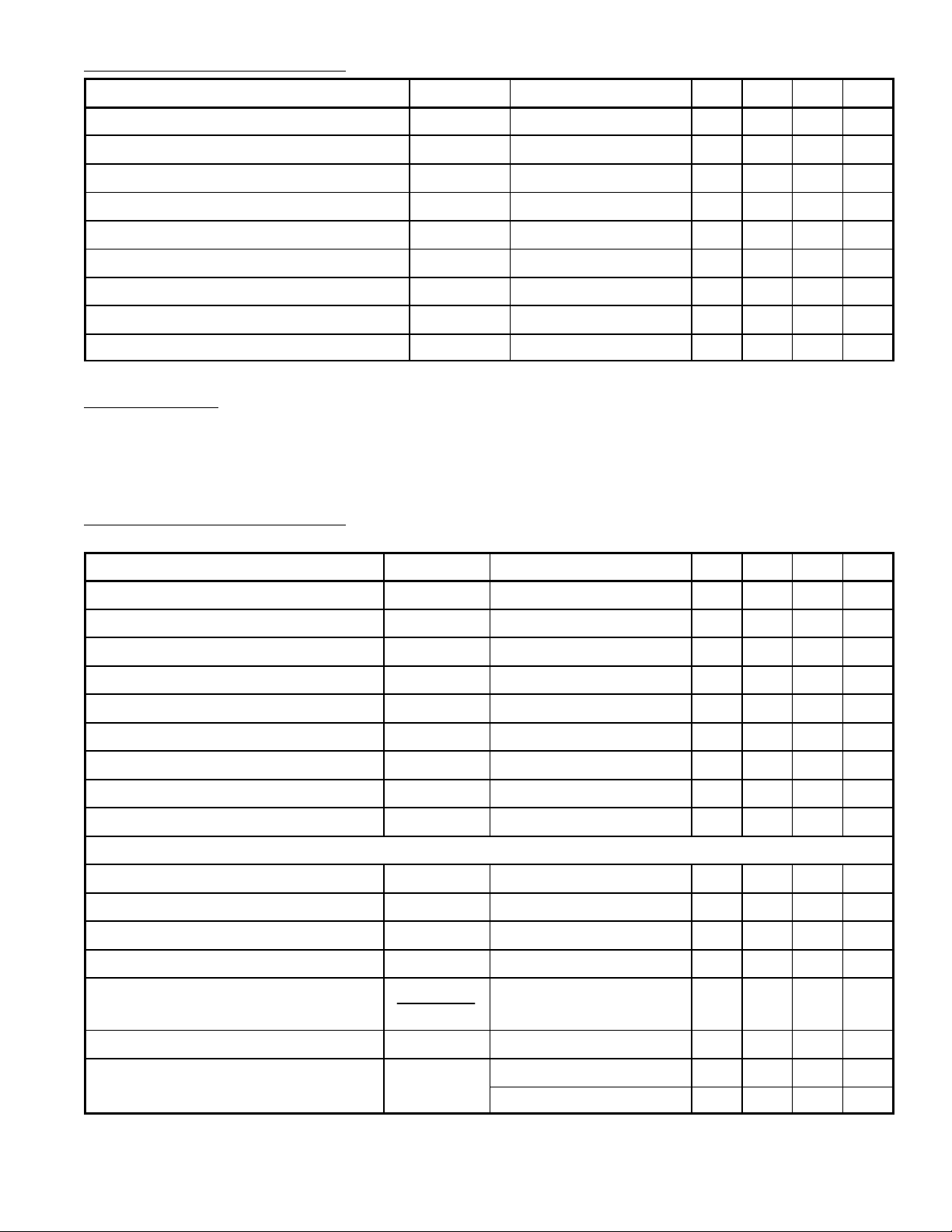
DC Electrical Characteristics: (VCC = 8.5V, TA = +25°C unless otherwise specified)
Parameter Symbol Test Conditions Min Typ Max Unit
Current Consumption (Without LED Driver) I
TOT
Power Dissipation P
Voltages on Pin15 V
Voltages on Pin16, Pin12 V
16–5
DC Current Pin14 –I
DC Current Pin2 –I
Output Current Pin3 –I
Switch “VCO OFF” Voltage (Pin7) V
Current (Pin7) I
D
15–5
, V
14
2
3
7
7
12–5
– 15 – mA
– 125 – mW
– 2.0 – V
– 3.5 – V
195 275 390 µA
195 275 390 µA
– – 20 mA
– 2.2 – V
– – 50 µA
AF Conditions:
Input MUX signal is 1V
= 1kHz; V
P–P
= 32mV (9%), oscillator adjusted t o f
PILOT
= 228kHz at VI = 0V,
OSC
unless otherwise specified. (All figures are measured with a roll–off network of 50kHz (2dB down at
38kHz) at the input.
AC Electrical Characteristics:
Parameter Symbol Test Conditions Min Typ Max Unit
(All parameters are measured in the circuit at nominal supply
voltage(V
= 8.5V) and TA = +25°C)
CC
Gain Input Amplifier A
Input Impedance (External) Z
Maximum Input Voltage V
Gain Output Buffers A
V
I
I
V
– – 20 dB
– 47 – kΩ
– – TBD V
P–P
– 10 – dB
Maximum Output Voltage VO12, 16 THD ≤ 1% – – TBD V
Output Impedance Z
Maximim Load Impedance Z
O
L
Pin12, Pin16 – – 500 Ω
5.0 – – kΩ
Muting Level α muting – 90 – dB
Source Selector α – 90 – dB
Overall Performance
Overall Gain (Mono) V
OUT/VIN
10 11 12 dB
AF Output Voltage (RMS) Mono V12 = V16 1.1 1.25 – V
Total Harmonic Distortion THD V
Output Voltage V
Output Channel Unbalance
12, 16 THD = 1% – – TBD V
OUT
V
12
OUT
V
16
OUT
OUT
= 1.2V
, Note 1 – – 0.5 %
RMS
– 0.2 1.0 dB
Channel Separation α L = 1, R = 0 26 40 – dB
0
Signal–to–Noise Ratio S/N Bandwidth 20Hz to 16kHz – 76 – dB
Bandwidth DINA – 82 – dB
Note 1. Guaranteed for mono, mono +pilot, stereo.
Page 3

AC Electrical Characteristics (Cont’d): (All parameters are measured in the circuit at nominal
supply voltage(V
Parameter Symbol Test Conditions Min Typ Max Unit
SDS Control
10dB Channel Separation V4 – 1.0 – V
Full Stereo V4 Channel Separation ≥ 26dB – 1.2 – V
Full Mono V4 Channel Separation ≥ 1dB – 0.8 – V
Stereo/Mono Switch (R6 – 5 = 180k, Note 2)
= 8.5V) and TA = +25°C)
CC
For Switching to Stereo V
For Switching to Mono V
Hysteresis ∆V
Carrier and Harmonic Suppression at the Output (Note 3)
Pilot Signal α19 f = 19kHz, R6–5 = 180kΩ, Note 2 32 40 – dB
Subcarrier α38 f = 38kHz – 45 – dB
Intermodulation α2 fM = 10kHz, spurious signal,
Traffic Radio (VWF) Suppression α57 (VWF) f = 57kHz, Note 5 – 80 – dB
SCA (Subsidary Communications
Authorization)
I
I
I
α57 f = 57kHz – 50 – dB
α228 f = 228kHz – 75 – dB
= 1kHz, Note 4
f
S
α3 fM = 13kHz, spurious signal,
= 1kHz, Note 4
f
S
α67 f = 67kHz, Note 6 – 70 – dB
– 14 20 mV
4 – – mV
– 4 – mV
– 50 – dB
– 50 – dB
Note 2. Also adjustable.
Note 3. Reference output voltage at 1kHz (measured channel R (Pin2)).
Note 4. Intermodulation suppression (BFC: Beat–Frequency Components):
(signal) at 1kHz
V
α2 = : f
α3 = : fS = (3 x 13kHz) – 38kHz
O
V
(spurious) at 1kHz
O
(signal) at 1kHz
V
O
V
(spurious) at 1kHz
O
= (2 x 10kHz) – 19kHz
S
measured with: 91% mono signal; fM = 10 or 13kHz; 9% pilot signal.
Note 5. Traffic ratio (VWF) suppression:
(signal) at 1kHz
V
α57 (VWF) =
V
O
(spurious) at 1kHz ±23Hz
O
measured with: 91% stereo signal; fM = 1kHz; 9% pilot signal; 5% traffic subcarrier
(f = 57kHz; 60% AM modulated with f mod. 23Hz).
Note 6. SCA (Subsidary Communications Authorization):
(signal) at 1kHz
V
α67 =
measured with: 81% mono signal; f
(f
= 67kHz, unmodulated).
S
O
V
(spurious) at 9kHz
O
fS = (2 x 38kHz) – 67kHz
= 1kHz; 9% pilot signal; 10% SCA–subcarrier
M
Page 4

AC Electrical Characteristics (Cont’d): (All parameters are measured in the circuit at nominal
supply voltage(V
Parameter Symbol Test Conditions Min Typ Max Unit
Carrier and Harmonic Suppression at the Output (Cont’d) (Note 3)
ACI (Adjacent Channel Interference) α114 f = 114kHz, Note 7 – 90 – dB
α190 f = 190kHz, Note 7 – 60 – dB
= 8.5V) and TA = +25°C)
CC
Ripple Rejection RR100
f = 100Hz,
V
RIPPLE
= 100mV
V9 = 8.5V – 46 – dB
V9 = 7.0V – TBD – dB
VCO (Voltage–Controlled Oscillator)
Oscillator Frequency Adjustable
f
OSC
with R8
Capture Range (Deviation from
∆f/f V
= 32mV – 4 – %
PILOT
228kHz Center Frequency)
Temperature Drift (Uncompensated) T
C
Muting Circuit (Pin11)
Input Voltage (Mute “ON”) V
Input Voltage (Mute “OFF”) V
Input Current (Mute “ON”) –I
Input Current (Mute “OFF”) I
Dlow
Dhigh
Dlow
Dhigh
Source Selector (Pin10) Switching Level
Cassette–to–Radio V
Radio–to–Cassette V
Clow
–I
Clow
Chigh
I
Chigh
Note 3. Reference output voltage at 1kHz (measured channel R (Pin2)).
Note 7. ACI (Adjacent Channel Interference):
– 228 – kHz
– +200 – ppm/°C
– – 0.8 V
2.0 – 8.0 V
25 10 – µA
– – TBD µA
– – 0.8 V
25 10 – µA
2.0 – 8.0 V
– – TBD µA
(signal) at 1kHz
V
α114 = : f
α190 = : fS = 186kHz – (3 x 38kHz)
O
V
(spurious) at 4kHz
O
(signal) at 1kHz
V
O
V
(spurious) at 4kHz
O
= 110kHz – (3 x 38kHz)
S
measured with: 90% mono signal; fS = 1kHz; 9% pilot signal; 1% spurious signal
= 110 or 186kHz, unmodulated).
(f
S
Page 5

Pin Connection Diagram
Cassette Input
(R) Stereo
DEC Output
LED Driver
SDS Control
1
2
3
4
5GND
Pilot Cancel/
Level Control
VCO
OFF
6
7
8OSC
16 9
16
(R) Output
MUX Input
15
(L) Stereo
14
DEC Output
Cassette Input
13
12 (L) Output
11 Mute
Radio/Cassette
10
Switch
9
V
CC
18
.870 (22.0) Max .260 (6.6)
Max
.200 (5.08)
Max
.100 (2.54)
.099 (2.5) Min
.700 (17.78)
 Loading...