

Page 1
NTE7006
Integrated Circuit
Switch Mode Driver for DC Motors
Description
The NTE7006 is a monolithic LSI circuit in 15–Lead SIP type package with staggered leads. This
device is intended for use in a 3–chip DC motor positioning system for applications such as carriage/
daisy–wheel position control in typewriters.
Features
D Driving Capability: 2A, 36V, 30kHz
D 2 Logic Chip Enable
D External Loop Gain Adjustment
D Single Power Supply: 18V to 36V
D Input Signal Symmetric to GND
D Thermal Protection
Absolute Maximum Ratings:
Power Supply, V
Input Voltage, V
Inhibit voltage, V
Total Power Dissipation (TC = +75°C), P
S
I
inhibit
tot
Operating Junction Temperature Range, T
Storage Temperature Range, T
stg
Thermal Resistance, Junction–to–Case, R
opr
Θ
–15V to +VS V. . . . . . . . . . . . . . . . . . . . . . . . . . . . . . . . . . . . . . . . . . . . . . . . . . . . . . . . .
–40° to +150°C. . . . . . . . . . . . . . . . . . . . . . . . . . . . . . . .
–40° to +150°C. . . . . . . . . . . . . . . . . . . . . . . . . . . . . . . . . . . . . . . . . .
JC
36V. . . . . . . . . . . . . . . . . . . . . . . . . . . . . . . . . . . . . . . . . . . . . . . . . . . . . . . . . . . . . . . . . . . . . . . . . . . . . . . . . . .
0 to VS V. . . . . . . . . . . . . . . . . . . . . . . . . . . . . . . . . . . . . . . . . . . . . . . . . . . . . . . . . .
25W. . . . . . . . . . . . . . . . . . . . . . . . . . . . . . . . . . . . . . . . . . . .
3°C/W. . . . . . . . . . . . . . . . . . . . . . . . . . . . . . . . . . . . . . .
Electrical Characteristics: (TA = +25°C, f
Parameter Symbol Test Conditions Min Typ Max Unit
Supply Voltage V
Quiescent Drain Current I
Input Offset Voltage (Pin6) V
Inhibit Low Level (Pin12, Pin13) V
Inhibit High Level (Pin12, Pin13) V
S
d
OS
inh
inh
= 20kHz unless otherwise specified)
OSC
18 – 36 V
VS = 20V (Offset Null) – 30 50 mA
VS = 36V, IO = 0 – – ±350 mV
– – 2 V
3.2 – – V
Page 2
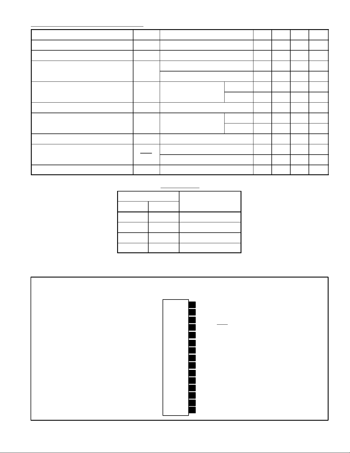
Electrical Characteristics (Cont’d): (TA = +25°C, f
Parameter Symbol Test Conditions Min Typ Max Unit
= 20kHz unless otherwise specified)
OSC
Low Voltage Condition I
High Voltage Conditions I
Input Current (Pin6) I
Input Voltage (Pin6) V
Output Current I
Total Dropout Voltage V
Sensing Resistor Voltage Drop V
Transconductance
Frequency Range (Pin10) f
OSC
V
inhibit
Pin12 Pin13
inh
inh
O
RS
I
O
V
V
(L) = 0.4V – – –100 µA
inh
V
inh (H) = 3.2V
VI = –8.8V – – –1.8 mA
I
– – 10 µA
VI = +8.8V – – 0.5 mA
RS1 = RS2 = 0.2Ω IO = 2A – 8.3 – V
I
IO = –2A – –8.3 – V
VI = ±8.8V, RS1 = RS2 = 0.2Ω ±2 – – A
(Including Sensing
D
Resistors)
IO = 2A – – 5 V
IO = 1A – – 3.5 V
TJ = +150°C, IO = 2A – – 0.44 V
RS1 = RS2 = 0.2Ω 228 240 260 mA/V
RS1 = RS2 = 0.4Ω – 120 – mA/V
i
1 – 30 kHz
Truth Table:
Output Stage
Condition
L L Disabled
L H Normal Operation
H L Disabled
H H Disabled
Note 1. The output stage is also disabled
if the supply voltage falls below
18V.
Pin Connection Diagram
(Front View)
15
14
13
12
11 OSC (R)
10
Motor
R
S2
Inhibit (CE1)
Inhibit (CE2)
OSC (C)
Output (Error Amp)
9
GND
8
Input (Error Amp)7
Input
6
Output C.S.A.
5
Comp Input4
(+) V
3
2
S
R
S1
Motor1
Page 3
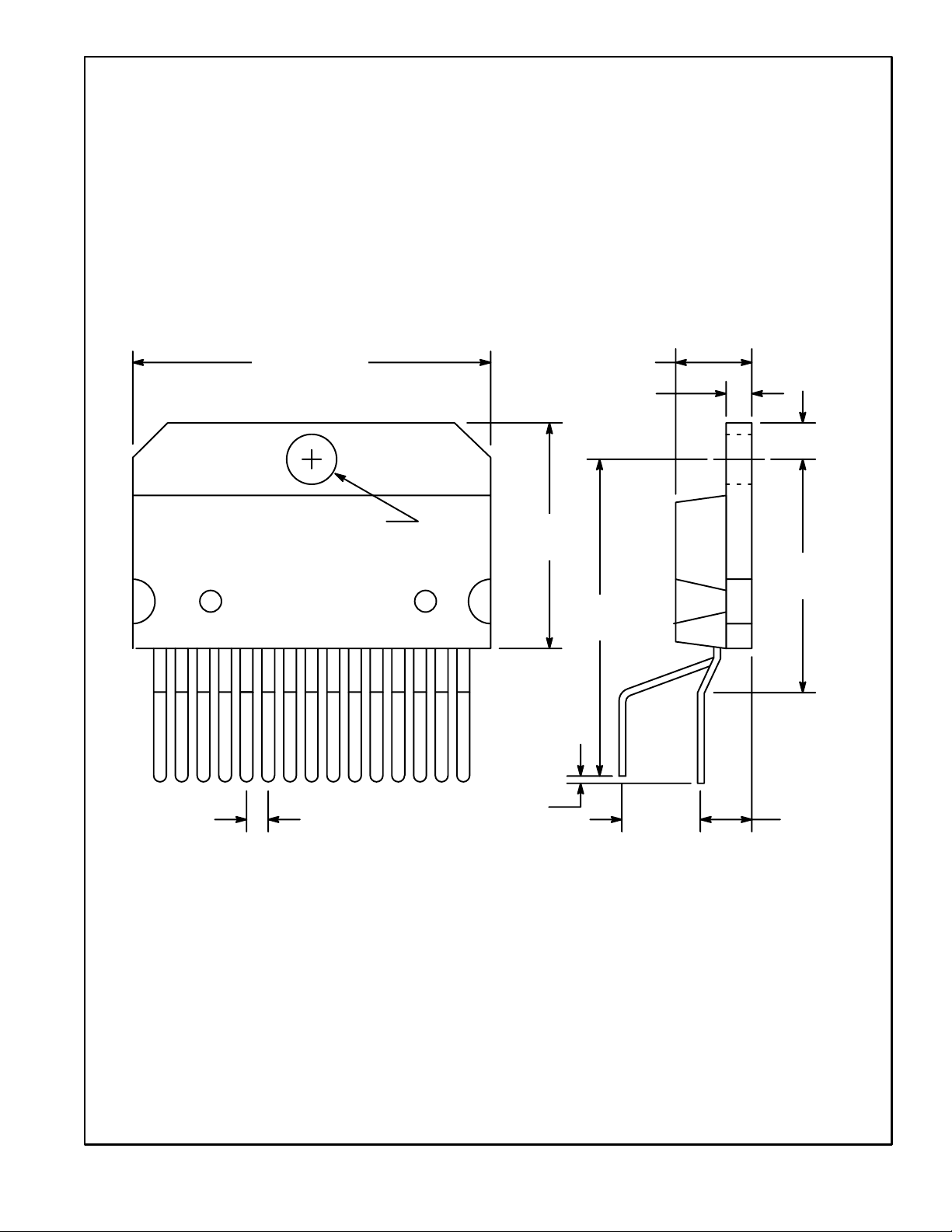
.791 (20.1)
.196 (4.99)
.069 (1.75)
.110
(2.79)
.150 (3.81) Dia Max
.050 (1.27) .200
.689
(17.5)
151
.008 (.203)
.860
(21.8)
(5.08)
.699
(17.7)
.169
(4.29)
 Loading...