

Page 1

NTE7119
Integrated Circuit
22W BTL (2 x 11W) Stereo Power Amplifier
Description:
The NTE7119 integrated circuit is a class–B dual output amplifier in a 9–Lead SIP type package designed primarily for use in car radio applications. This device contains two identical amplifiers with
differential input stages. The gain of each amplifier is fixed at 40dB.
Features:
D Stereo or BTL Application
D Few External Components for BTL
D High Output Power
D Low Offset Voltage at Output
D Fixed Gain
D Good Ripple Rejection
D Mute/Stand–by Switch
Absolute Maximum Ratings:
Supply Voltage, V
P
Operatring 18V. . . . . . . . . . . . . . . . . . . . . . . . . . . . . . . . . . . . . . . . . . . . . . . . . . . . . . . . . . . . . . . . . . .
Non–Operating 30V. . . . . . . . . . . . . . . . . . . . . . . . . . . . . . . . . . . . . . . . . . . . . . . . . . . . . . . . . . . . . .
Load Dump Protected (during 50ms, t
AC and DC Short–Circuit Safe Voltage, V
Reverse Polarity, V
PR
Energy Handling Capability at Outputs (V
Non–Repetitive Peak Output Current, I
Repetitive Peak Output Current, I
Total Power Dissipation, P
Crystal Temperature, T
Storage Temperature Range, T
tot
C
stg
OSM
ORM
≥ 2.5ms) 45V. . . . . . . . . . . . . . . . . . . . . . . . . . . . . . . . . .
r
PSC
= 0V) 200mJ. . . . . . . . . . . . . . . . . . . . . . . . . . . . . . . . . . . .
P
D Load Dump Protection
D Thermally Protected
D Reverse Polarity Safe
D Ability to Handle High Energy on Outputs
D No Switch–ON/OFF Pop
D Low Thermal Resistance
D Short Circuit Protected
18V. . . . . . . . . . . . . . . . . . . . . . . . . . . . . . . . . . . . . . . . . .
6V. . . . . . . . . . . . . . . . . . . . . . . . . . . . . . . . . . . . . . . . . . . . . . . . . . . . . . . . . . . . . . . .
6A. . . . . . . . . . . . . . . . . . . . . . . . . . . . . . . . . . . . . . . . . . . . .
4A. . . . . . . . . . . . . . . . . . . . . . . . . . . . . . . . . . . . . . . . . . . . . . . . . .
25W. . . . . . . . . . . . . . . . . . . . . . . . . . . . . . . . . . . . . . . . . . . . . . . . . . . . . . . .
+150°C. . . . . . . . . . . . . . . . . . . . . . . . . . . . . . . . . . . . . . . . . . . . . . . . . . . . . . . . .
–65° to +150°C. . . . . . . . . . . . . . . . . . . . . . . . . . . . . . . . . . . . . . . . . .
Page 2
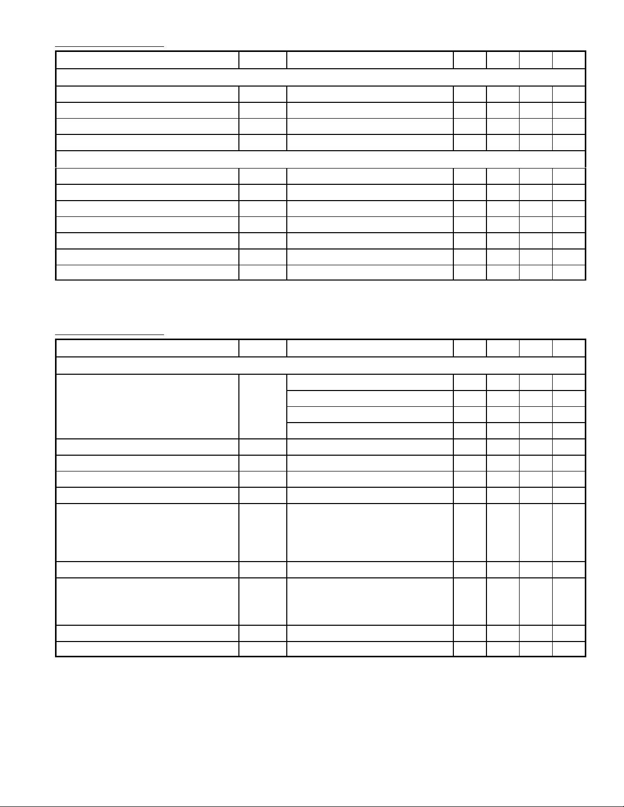
DC Characteristics: (VP = 14.4V, TA = +25°C unless otherwise specified)
Parameter Symbol Test Conditions Min Typ Max Unit
Supply
Supply Voltage Range V
Total Quiescent Current I
DC Output Voltage V
DC Output Offset Voltage |∆V
tot
Note 1 6.0 14.4 18.0 V
P
– 40 80 mA
Note 2 – 6.95 – V
O
| – – 250 mV
4–6
Mute/Stand–by Switch
Switch–ON Voltage Level V
Mute Condition V
Output Signal in Mute Position V
DC Output Offset Voltage |∆V
Stand–by Condition V
DC Current in Stand–by Condition I
Switch–ON Current I
ON
mute
VI = 1V (max), f = 20Hz to 15kHz – – 20 mV
O
| – – 250 mV
4–6
sb
sb
sw
8.5 – – V
3.3 – 6.4 V
0 – 2 V
– – 100 µA
– 12 40 µA
Note 1. The circuit is DC adjusted at VP = 6V to 18V and AC operating at VP = 8.5V to 18V.
Note 2. At 18V < V
< 30V the DC output voltage ≤ VP/2.
P
AC Characteristics: (VP = 14.4V, RL = 4Ω, f = 1kHz, TA = +25°C unless otherwise specified)
Parameter Symbol Test Conditions Min Typ Max Unit
Stereo Application
Output Power P
THD = 0.5%, Note 3 4 5 – W
O
THD = 10%, Note 3 5.5 6.0 – W
THD = 0.5%, RL = 2Ω, Note 3 7.5 8.5 – W
THD = 10%, RL = 2Ω, Note 3 10 11 – W
Total Harmonic Distortion THD PO = 1W – 0.1 – %
Low Frequency Roll–Off f
High Frequency Roll–Off f
Closed Loop Voltage Gain G
Supply Voltage Ripple Rejection
RR
ON
Mute
Standby
–3dB, Note 4 – 45 – Hz
L
–1dB, Note 4 20 – – kHz
H
V
Note 5, Note 6
Note 5, Note 7
Note 5, Note 6, Note 7
Note 5, Note 6, Note 7
39 40 41 dB
40
45
45
80
–
–
–
–
–
dB
–
dB
–
dB
–
dB
Input Impedance |Zi| 50 60 75 kΩ
Noise Output Voltage (RMS Value)
ON
Mute
V
no(rms)
RS = 0Ω, Note 8
R
= 10kΩ, Note 8
S
Note 9
–
150
–
250
–
120
–
500
–
µV
µV
µV
Channel Separation α RS = 10kΩ 40 – – dB
Channel Unbalance |∆GV| – 0.1 1 dB
Note 3. Output power is measured directly at the output pins of the IC.
Note 4. Frequency response externally fixed.
Note 5. Ripple rejection measured at the output with a source impedance of 0Ω (maximum ripple
amplitude of 2V)
Note 6. Frequency f = 100Hz.
Note 7. Frequency between 1kHz and 10kHz.
Note 8. Noise voltage measured in a bandwidth of 20Hz to 20kHz.
Note 9. Noise output voltage independent of R
(VI = 0V).
S
Page 3

AC Characteristics: (VP = 14.4V, RL = 4Ω, f = 1kHz, TA = +25°C unless otherwise specified)
Parameter Symbol Test Conditions Min Typ Max Unit
BTL Application
Output Power P
Total Harmonic Distortion THD PO = 1W – 0.1 – %
Power Bandwidth B
Low Frequency Roll–Off f
High Frequency Roll–Off f
Closed Loop Voltage Gain G
Supply Voltage Ripple Rejection
ON
Mute
Standby
Input Impedance |Zi| 25 30 38 kΩ
Noise Output Voltage (RMS Value)
ON
Mute
RR
V
no(rms)
THD = 0.5%, Note 3 15 17 – W
O
THD = 10%, Note 3 20 22 – W
THD = 0.5%, VP = 13.2V, Note 3 – 13 – W
THD = 10%, VP = 13.2V, Note 3 – 17.5 – W
THD = 0.5%, PO = –1dB, w.r.t 15W 35 to 15,000 Hz
W
–1dB, Note 4 – 45 – Hz
L
–1dB, Note 4 20 – – kHz
H
V
Note 5, Note 6
Note 5, Note 7
Note 5, Note 6, Note 7
Note 5, Note 6, Note 7
RS = 0Ω, Note 8
R
= 10kΩ, Note 8
S
Note 9
45 46 47 dB
34
48
48
80
–
–
–
–
–
–
–
200
350
180
–
–
–
–
–
700
–
dB
dB
dB
dB
µV
µV
µV
Note 3. Output power is measured directly at the output pins of the IC.
Note 4. Frequency response externally fixed.
Note 5. Ripple rejection measured at the output with a source impedance of 0Ω (maximum ripple
amplitude of 2V)
Note 6. Frequency f = 100Hz.
Note 7. Frequency between 1kHz and 10kHz.
Note 8. Noise voltage measured in a bandwidth of 20Hz to 20kHz.
Note 9. Noise output voltage independent of R
(VI = 0V).
S
Page 4

Pin Connection Diagram
(Front View)
Non–Invert Input
1
GND (Signal)
2
RR
3
4
Output 1
5 GND (Substrate)
6 Output 2
V
7
8
Mute/Stand–by Switch
Invert Input9
P
.961 (24.4)
.780 (19.8) .185 (4.7)
.489
(12.4)
.079
91
(2.0)
.674
(17.0)
.100 (2.54).079 (2.0)
 Loading...