

Page 1

NTE3880
Integrated Circuit
NMOS, 8–Bit Microprocessor (MPU), 4MHz
Description:
The NTE3880 is a third generation single chip microprocessor with unrivaled computational power.
This increased computational power results in higher system through–put and more efficient memory
utilization when compared to second generation microprocessors. In addition it is very easy to implement into a system because of it’ s single voltage requirement plus all output signals are fully decoded
and timed to control standard memory or peripheral circuits. The circuit is implemented using an N–
channel, ion implanted, silicon gate MOS process.
This device has an internal register configuration which contains 208 bits of Read/Write memory that
are accessible to the programmer. The registers include two sets of six general purpose registers that
may be used individually as 8–bit registers or as 16–bit register pairs. There are also two sets of accumulator and flag registers. The programmer has access to either set of main or alternate registers
through a group of exchange instructions. This alternate set allows foreground/background mode of
operation or may be reserved for very fast interrupt response. The NTE3880 also contains a 16–bit
stack pointer which permits simple implementation of multiple level interrupts, unlimited subroutine
nesting and simplification of many types of data handling.
The two 16–bit index registers allow tabular data manipulation and easy implementation of relocatable code. The Refresh register provides for automatic, totally transparent refresh of external dynamic memories. The I register is used in a powerful interrupt response mode to form the upper 8 bits of
a pointer to a interrupt service address table, while the interrupting device supplies the lower 8 bits
of the pointer. An indirect call is then made to this service address.
Features:
D Single Chip, N–Channel Silicon Gate
D 158 Instructions – Includes all 78 of the 8080A Instructions with T otal Software Compatibility. N e w
Instructions Include 4–, 8– and 16–Bit Operations with more useful Addressing Modes such as
Indexed, Bit and Relative
D 17 Internal Registers
D Three Modes of Fast Interrupt Response plus a Non–Maskable Interrupt
D Directly Interfaces Standard Speed Static or Dynamic Memories with Virtually No External Logic
D 1.0µs Instruction Execution Speed
D Single 5VDC Supply and Single–Phase 5V Clock
D Out–Performs any other Single–Phase 5V Clock
D All Pins TTL Compatible
D Built–In Dynamic RAM Refresh Circuitry
Page 2
Absolute Maximum Ratings:
Temperature Under Bias 0° to +70°C. . . . . . . . . . . . . . . . . . . . . . . . . . . . . . . . . . . . . . . . . . . . . . . . . . . . .
Storage Temperature Range –65° to +150°C. . . . . . . . . . . . . . . . . . . . . . . . . . . . . . . . . . . . . . . . . . . . . . .
Voltage On Any Pin With Respect to GND –0.3V to +7V. . . . . . . . . . . . . . . . . . . . . . . . . . . . . . . . . . . . .
Power Dissipation 1.5W. . . . . . . . . . . . . . . . . . . . . . . . . . . . . . . . . . . . . . . . . . . . . . . . . . . . . . . . . . . . . . . . .
Note 1. Stresses above those listed under “Absolute Maximum Ratings” may cause permanent
damage to the device. This is a stress rating only functional operation of the device at these
or any other condition above those indicated in the operational sections of this specification
is not implied. Exposure to absolute maximum rating conditions for extended periods may
affect device reliability.
DC Characteristics: (TA = 0° to 70°C, VCC = 5V ±5% unless otherwise specified)
Parameter Symbol Test Conditions Min Typ Max Unit
Clock Input Low Voltage V
Clock Input High Voltage V
Input Low Voltage V
Input High Voltage V
Output Low Voltage V
Output High Voltage V
Power Supply Current I
Input Leakage Current I
Tri–State Output Leakage Current in Float I
Tri–State Output Leakage Current in Float I
Data Bus Leakage Current in Input Mode I
ILC
IHC
IL
IH
OL
OH
CC
L1
LOH
LOL
LD
IOL = 1.8mA – – 0.4 V
IOH = –250µA 2.4 – – V
VIN = 0 to V
V
OUT
V
OUT
0 ≤ VIN ≤ V
CC
= 2.4 to V
CC
= 0.4V – – –10 µA
CC
–0.3 – 0.80 V
VCC–0.6 – VCC+3 V
–0.3 – 0.8 V
2.0 – V
CC
– 90 200 mA
– – 10 µA
– – 10 µA
– – ±10 µA
V
Capacitance: (TA = +25°C, f = 1MHz, unmeasured pins to GND unless otherwise specified)
Parameter Symbol Test Conditions Min Typ Max Unit
Clock Capacitance C
Input Capacitance C
Output Capacitance C
φ
IN
OUT
– – 35 pF
– – 5 pF
– – 10 pF
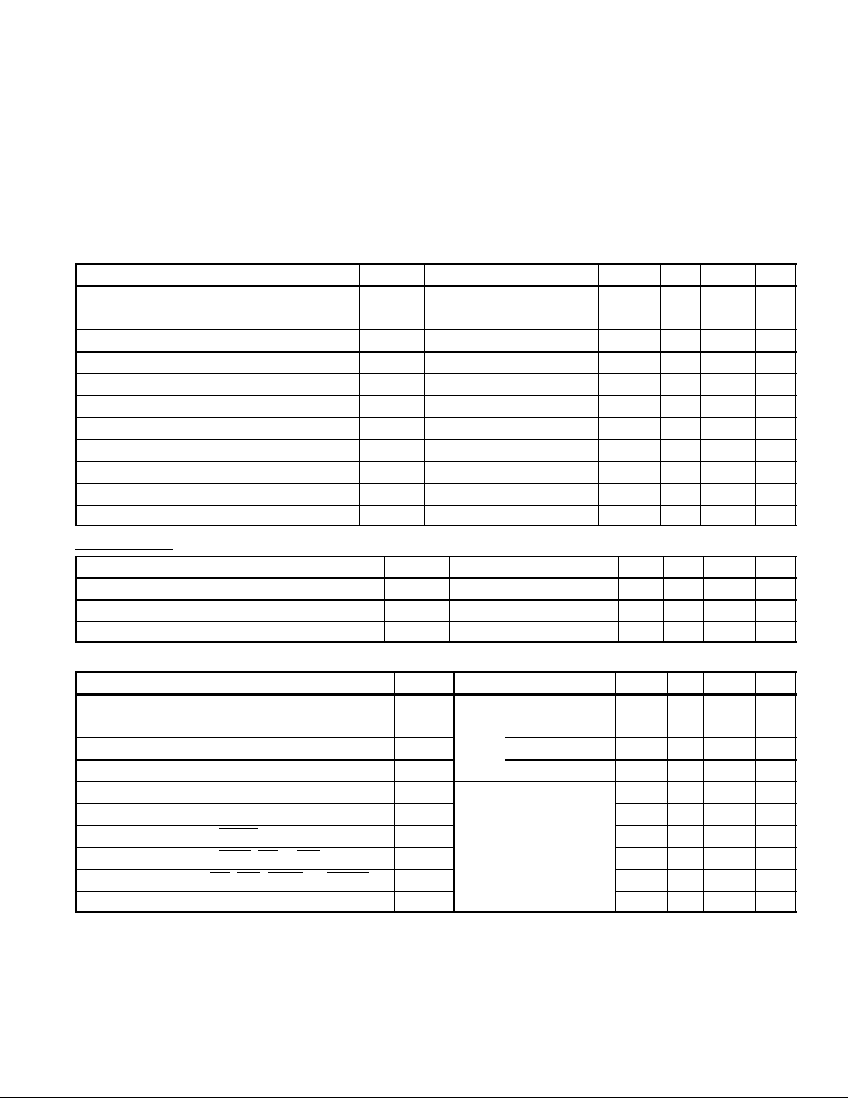
AC Characteristics: (TA = 0°C to +70°C, VCC = +15V ± 5% unless otherwise specified)
Parameter Symbol Signal Test Conditions Min Typ Max Unit
Clock Period t
c
Clock Pulse Width, Clock High tw (φH)
Clock Pulse Width, Clock Low tw (φL) 110 – 2000 ns
Clock Rise and Fall Time tr, t
f
Address Output Delay tD (AD) A
Data to Float tF (AD) – – 90 ns
Address Stable Prior to MRFQ (Memory Cycle) t
Address Stable Prior to IOFQ, RD or WR (I/O Cycle) t
Address Stable from RD, WR, IORQ, or MREQ t
Address Stable from RD or WR During Float t
Note 2. tc = t
(φH) + t
w
(φL) + tr + tf.
w
acm
aci
ca
caf
Note 3. Although static by design, testing guarantees t
Note 4. t
Note 5. t
Note 6. tca = t
Note 7. t
= t
acm
= tc–70.
aci
= t
caf
(φH) + tf–65.
w
(φL) + tr–50.
w
(φL) + tr–45.
w
φ 25 – Note 2 µs
110 – Note 3 ns
– – 30 ns
0–15CL
= 50pF – – 110 ns
Note 4 – – ns
Note 5 – – ns
Note 6 – – ns
Note 7 – – ns
(φH) of 200µs maximum.
w
Page 3

AC Characteristics (Cont’d): (TA = 0°C to +70°C, VCC = +15V ± 5% unless otherwise specified)
Parameter Symbol Signal Test Conditions Min Typ Max Unit
Data Output Delay tD (D) D
Delay to Float During Write Cycle tF (D)
Data Setup Time to Rising Edge of Clock
t
(D) 35 – – ns
φ
S
During M1 Cycle
Data Setup Time to falling Edge of Clock
During M2 to M
Data Stable Prior to WR (Memory Cycle) t
Data Stable Prior to WR (I/O Cycle) t
Data Stable From WR t
Any Hold Time for Setup Time t
MREQ Delay From Falling Edge of Clock,
5
dcm
dci
cdf
H
t
(MR) MREQ CL = 50pF – – 85 ns
φ
DL
MREQ Low
MREQ Delay From Rising Edge of Clock,
t
(MR) – – 85 ns
φ
DH
MREQ High
MREQ Delay From Falling Edge of Clock,
MREQ High
Pulse Width, MREQ Low tw (MRL) Note 11 – – ns
Pulse Width, MREQ High tw (MRH) Note 12 – – ns
IORQ Delay From Rising Edge of Clock
t
(IR) IORQ CL = 50pF – – 75 ns
φ
DL
IORQ Low
IORQ Delay From Falling Edge of Clock
IORQ Low
IORQ Delay From Rising Edge of Clock
t
(IR) – – 85 ns
φ
DH
IORQ High
IORQ Delay From Falling Edge of Clock
IORQ High
RD Delay From Rising Edge of Clock,
t
(RD) RD CL = 50pF – – 85 ns
φ
DL
RD Low
RD Delay From Falling Edge of Clock,
RD Low
RD Delay From Rising Edge of Clock,
t
(RD) – – 85 ns
φ
DH
RD High
RD Delay From Falling Edge of Clock,
RD High
WR Delay From Rising Edge of Clock,
t
(WR) WR CL = 50pF – – 65 ns
φ
DL
WR Low
WR Delay From Falling Edge of Clock,
WR Low
WR Delay From Falling Edge of Clock,
t
(WR) – – 80 ns
φ
DH
WR High
Pulse Width, WR Low tw (WRL) Note 13 – – ns
CL = 50pF – – 150 ns
0–7
– – 90 ns
50 – – ns
Note 8 – – ns
Note 9 – – ns
Note 10 – – ns
– – 0 ns
– – 85 ns
– – 85 ns
– – 85 ns
– – 95 ns
– – 85 ns
– – 80 ns
Note 8. t
Note 9. t
Note10. t
Note11. t
Note12. t
= tc–170.
dcm
= t
(φL) + tr–170.
dci
cdf
w
w
w
= t
(φL) + tr–70.
w
(MRL) = tc–30.
(MRH) = t
(φH) + tr–20.
w
Note13. tw (WRL) = tc–30.
Page 4

AC Characteristics (Cont’d): (TA = 0°C to +70°C, VCC = +15V ± 5% unless otherwise specified)
Parameter Symbol Signal Test Conditions Min Typ Max Unit
M1 Delay From Rising Edge of Clock,
M1 Low
M1 Delay From Rising Edge of Clock,
M1 High
RFSH Delay From Rising Edge of Clock,
Low
RFSH
RFSH Delay From Rising Edge of Clock,
RFSH High
WAIT Setup Time to Falling Edge of Clock ts (WT) WAIT 70 – – ns
HAL T Delay Time From Falling Edge of Clock tD (HT) HALT CL = 50pF – – 300 ns
INT Setup Time to Rising Edge of Clock ts (IT) INT 80 – – ns
Pulse Width, NM1 Low tw (NML) NM1 80 – – ns
BUSRQ Setup Time to Rising Edge of Clock ts (BQ) BUSRQ 50 – – ns
BUSAK Delay From Rising Edge of Clock,
BUSAK Low
BUSAK Delay From Rising Edge of Clock,
BUSAK High
RESET Setup Time to Rising Edge of Clock ts (RS) RESET 60 – – ns
Delay to Float (MREQ, IORQ, RD and WR) tF (C) – – 80 ns
M1 Stable Prior to IORQ (Interrupt Ack.) t
tDL (M1) M1 CL = 50pF – – 100 ns
tDH (M1)
– – 100 ns
tDL (RF) RFSH CL = 50pF – – 130 ns
tDH (RF) – – 120 ns
tDL (BA) BUSAK CL = 50pF – – 100 ns
tDH (BA) – – 100 ns
mr
Note 14 – – ns
Note14. tmr = 2tc + tw (φH) + tf–65.
Note15. Da t a should be enabled onto the CPU data bus w hen RD is active. During interrupt acknowl edge
data should be enabled when M1 and IORQ are both active.
Note16. All co ntrol si gnals are internally synchronized, so they may be totally asynchronous with
respect to the clock.
Note 17 . The RESET signal must be active for a minimum of 3 clock cycles.
Note 18 . Output Delay vs. Loaded Capacitance
TA = +70°CVCC = 5V ±5%
Add 10ns delay for each 50pf increase in load up to maximum of 200pF for data bus and
100pF for address & control lines.
Pin Connection Diagram
A
11
A
12
A
13
A
14
A
15
D
D
D
D
(+) 5V
D
D
D
D
INT
NMI
HALT
MREQ
IORQ
1
2
3
4
5
6System Clock Input
7
4
8
3
9 32
5
10
6
11
12 29
2
13 28
7
14 27
0
15 26
1
16
17
18 23
19 22
20 21
40
39
38
37
36
35
34
33
31
30
25
24
A
10
A
9
A
8
A
7
A
6
A
5
A
4
A
3
A
2
A
1
A
0
GND
RFSH
M
1
RESET
BUSRQ
WAIT
BUSAK
WD
RD
Page 5

40 21
120
2.055 (52.2)
.100 (2.54) .019 (0.5)
.155 (3.9)
.137
(3.5)
.550 (13.9)
Max
.650 (16.5)
 Loading...