

Page 1
NTE385
Silicon NPN Transistor
Audio Power Amp, Switch
Description:
The NTE385 is a silicon NPN transistor in a TO3 type package designed for high voltage, high speed,
power switching in inductive circuits where fall time is critical. It is particularly suited for line operated
switch mode applications.
Features:
D Fast Turn–Off Times
Absolute Maximum Ratings:
Collector–Emitter Voltage, V
Collector–Emitter Voltage (VBE = –1.5V), V
Emitter–Base Voltage, V
Collector Current, I
C
CEO(sus)
CEX
EB
Continuous 15A. . . . . . . . . . . . . . . . . . . . . . . . . . . . . . . . . . . . . . . . . . . . . . . . . . . . . . . . . . . . . . . . . .
Peak (Note 1) 30A. . . . . . . . . . . . . . . . . . . . . . . . . . . . . . . . . . . . . . . . . . . . . . . . . . . . . . . . . . . . . . . .
Overload 60A. . . . . . . . . . . . . . . . . . . . . . . . . . . . . . . . . . . . . . . . . . . . . . . . . . . . . . . . . . . . . . . . . . . .
Base Current, I
B
Continuous 5A. . . . . . . . . . . . . . . . . . . . . . . . . . . . . . . . . . . . . . . . . . . . . . . . . . . . . . . . . . . . . . . . . . .
Peak (Note 1) 20A. . . . . . . . . . . . . . . . . . . . . . . . . . . . . . . . . . . . . . . . . . . . . . . . . . . . . . . . . . . . . . . .
Total Power Dissipation (TC = +25°C), P
D
Derate Above 25°C 1.0W/°C. . . . . . . . . . . . . . . . . . . . . . . . . . . . . . . . . . . . . . . . . . . . . . . . . . . . . . .
Total Power Dissipation (TC = +100°C), P
Operating Junction Temperature Range, T
Storage Temperature Range, T
stg
Thermal Resistance, Junction–to–Case, R
D
J
thJC
Lead Temperature (During Soldering, 1/8” from case, 5sec), T
Note 1. Pulse test: Pulse Width = 5ms, Duty Cycle ≤ 10%.
–65° to +200°C. . . . . . . . . . . . . . . . . . . . . . . . . . . . . . . . . .
–65° to +200°C. . . . . . . . . . . . . . . . . . . . . . . . . . . . . . . . . . . . . . . . . .
L
400V. . . . . . . . . . . . . . . . . . . . . . . . . . . . . . . . . . . . . . . . . . . . . . . . .
850V. . . . . . . . . . . . . . . . . . . . . . . . . . . . . . . . . . . . . . . .
7V. . . . . . . . . . . . . . . . . . . . . . . . . . . . . . . . . . . . . . . . . . . . . . . . . . . . . . . . . . .
175W. . . . . . . . . . . . . . . . . . . . . . . . . . . . . . . . . . . . . . . . . . .
100W. . . . . . . . . . . . . . . . . . . . . . . . . . . . . . . . . . . . . . . . . .
1.0°C/W. . . . . . . . . . . . . . . . . . . . . . . . . . . . . . . . . . . . .
+275°C. . . . . . . . . . . . . . . . . . . . . . .
Electrical Characteristics: (TC = +25°C unless otherwise specified)
Parameter Symbol Test Conditions Min Typ Max Unit
OFF Characteristics (Note 2)
Collector–Emitter Sustaining Voltage V
Collector Cutoff Current I
Emitter Cutoff Current I
Emitter–Base Breakdown Voltage V
CEO(sus)IC
CEX
I
CER
EBO
(BR)EBOIE
= 200mA, IB = 0, L = 25mH 400 – – V
V
= 850V, V
CEX
V
= 850V, V
CEV
VCE = 850V, RBE = 10Ω – – 0.5 mA
VCE = 850V, RBE = 10Ω, TC = +1 00°C – – 3.0 mA
VBE = 5V, IC = 0 – – 0.1 mA
= 50mA, –IC = 0 7 – – V
= 1.5V – – 0.2 mA
BE(off)
= 1.5V, TC = +1 25°C – – 2.0 mA
BE(off)
Note 2. Pulse test: Pulse Width = 300µs, Duty Cycle ≤ 2%, Vcl = 300V, V
= 5V, LC = 180µH.
BE(off)
Page 2
Electrical Characteristics (Cont’d): (TC = +25°C unless otherwise specified)
Parameter Symbol Test Conditions Min Typ Max Unit
ON Characteristics (Note 2)
DC Current Gain h
Collector–Emitter Saturation Voltage V
Base–Emitter Saturation Voltage V
FE
CE(sat)IC
BE(sat)IC
Dynamic Characteristics
Output Capacitance C
ob
Switching Characteristics (Resistive Load)
Delay Time t
d
Rise Time t
Storage Time t
s
Fall Time t
Switching Characteristics (Inductive Load, Clamped)
Storage Time t
Fall Time t
Storage Time t
Crossover Time t
Fall Time t
sv
fi
sv
c
fi
VCE = 5V, IC = 10A 8 – –
= 10A, IB = 2A – – 1.5 V
IC = 10A, IB = 2A, TC = +1 00°C – – 2.0 V
IC = 8A, IB = 1.6A – – 1.5 V
IC = 8A, IB = 1.6A, TC = +1 00°C – – 2.0 V
= 10A, IB = 2A – – 1.6 V
IC = 10A, IB = 2A, TC = +1 00°C – – 1.6 V
VCB = 10V, IE = 0, f
= 1kHz – – 350 pF
test
VCC = 300V, IC = 10A, IB = 2A,
tp = 30µs, Duty Cycle = 2%,
r
V = 5V
V
= 5V
BE(off)
f
IC = 10A, IB1 = 2A, TC = +2 5°C
IC = 10A, IB1 = 2A, TC = +1 00°C
– 0.1 0.2 µs
– 0.4 0.7 µs
– 1.3 2.0 µs
– 0.2 0.4 µs
– 1.3 – µs
– 0.06 – µs
– 1.5 2.5 µs
– 0.3 0.6 µs
– 0.17 0.35 µs
Note 2. Pulse test: Pulse Width = 300µs, Duty Cycle ≤ 2%, Vcl = 300V, V
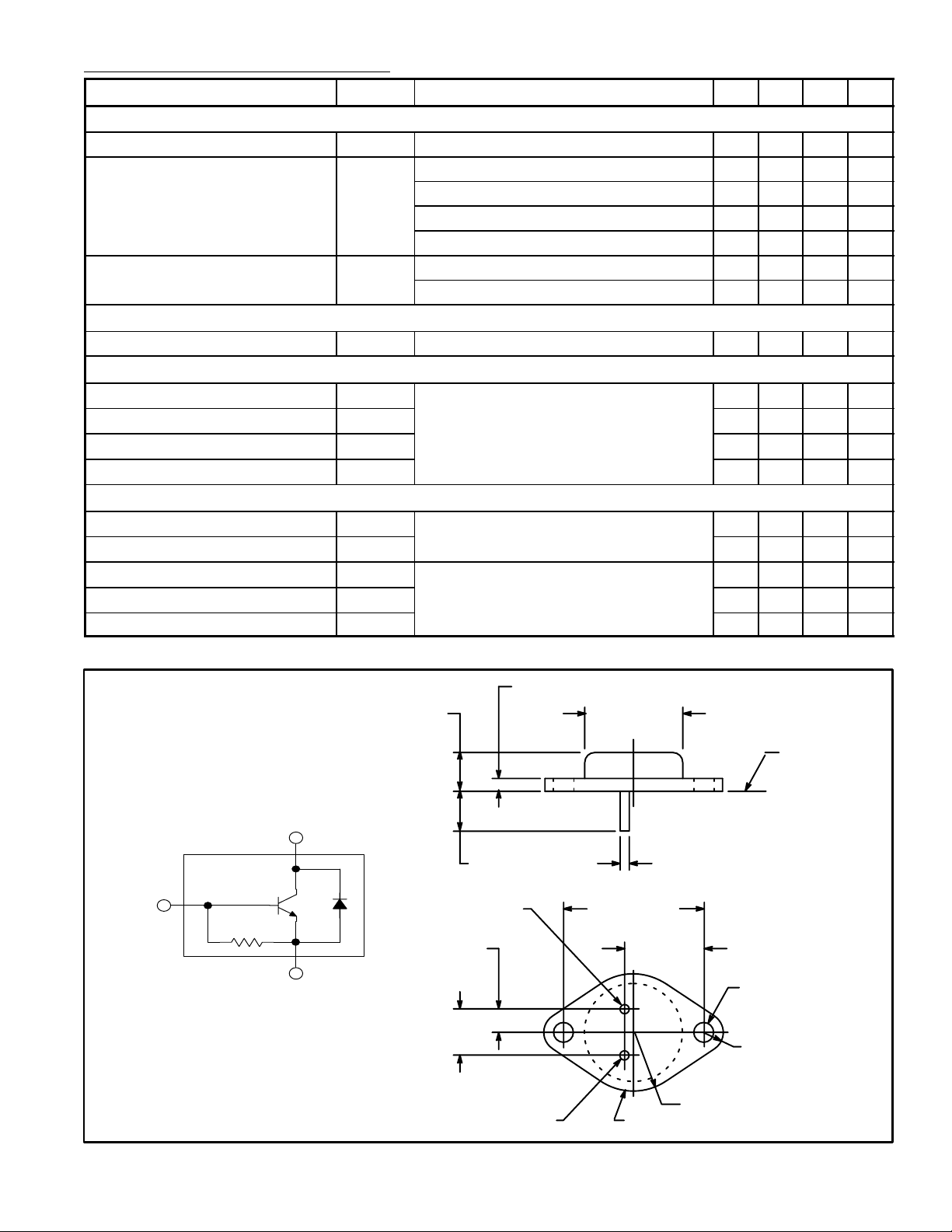
.135 (3.45) Max
BASE
.350 (8.89)
COLLECTOR
Emitter
.215 (5.45)
EMITTER
.430
(10.92)
.875 (22.2)
Dia Max
.040 (1.02).312 (7.93) Min
1.187
(30.16)
.665
(16.9)
Collector/CaseBase
= 5V, LC = 180µH.
BE(off)
Seating
Plane
.156 (3.96) Dia
(2 Holes)
.188 (4.8) R Max
.525 (13.35) R Max
 Loading...