

Page 1
NTE2114
Integrated Circuit
MOS, Static 4K RAM, 300ns
Description:
The NTE2114 1024–word 4–bit static random access memory is fabricated using N–channel silicon–
gate technology. All internal circuits are fully static and therefore require no clocks or refreshing for
operation. The data is read out nondestructively and has the same polarity as the input data. Common input/output pins are provided.
The separate chip select input (CS
) allows easy memory expansion by OR–tying individual devices
to a data bus.
Features
D All Inputs and Outputs Directly TTL Compatible
D Static Operation: No Clocks or Refreshing Required
D Low Power: 225mW Typ
D High Speed: Down to 300ns Access Time
D TRI–STATE Output for Bus interface
D Common Data In and Data Out Pins
D Single 5V Supply
D Standard 18–Lead DIP Package
Absolute Maximum Ratings:
Voltage at Any Pin –0.5V to +7V. . . . . . . . . . . . . . . . . . . . . . . . . . . . . . . . . . . . . . . . . . . . . . . . . . . . . . . . . .
Power Dissipation, P
Storage Temperature Range, T
Lead Temperature (During Soldering, 10sec), T
D
stg
L
–65° to +150°C. . . . . . . . . . . . . . . . . . . . . . . . . . . . . . . . . . . . . . . . . .
1W. . . . . . . . . . . . . . . . . . . . . . . . . . . . . . . . . . . . . . . . . . . . . . . . . . . . . . . . . . . . . .
+300°C. . . . . . . . . . . . . . . . . . . . . . . . . . . . . . . . . . . .
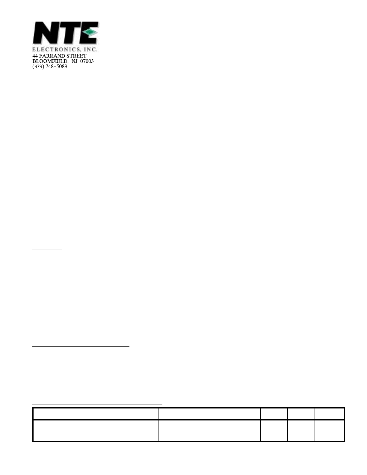
Recommended Operating Conditions:
Parameter Symbol Test Conditions Min Max Units
Supply Voltage V
Ambient temperature T
CC
A
4.75 5.25 V
0 +70 °C
Page 2
DC Electrical Characteristics: (TA = 0° to +70°, VCC = 5V ±5% unless otherwise specified)
Parameter
Logical “1” Input Voltage V
Logical “0” Input Voltage V
Logical “1” Output Voltage V
Logical “0” Output Voltage V
Input Load Current I
Output Leakage Current I
Power Supply Current I
Power Supply Current I
Symbol Test Conditions Min Max Units
IH
IL
OH
OL
LI
LO
CC1
CC2
2.0 V
CC
–0.5 0.8 V
IOH = –1.0mA 2.4 – V
IOL = 2.1mA – 0.4 V
VIN = 0 to 5.25V –10 10 µA
VO = 4V to 0.4V, CS = V
IH
–10 10 µA
All Inputs = 5.25V, TA = 25°C – 95 mA
All Inputs = 5.25V, TA = 0°C – 100 mA
V
AC Electrical Characteristics: (TA = 0°C to +70°C, VCC = 5V ±5%, Note 2 unless otherwise specified)
Parameter
Symbol Test Conditions Min Max Units
READ CYCLE
Read Cycle Time (WE = VIH) t
Access Time t
Chip Select to Output Valid t
Chip Select to Output Active t
Chip Select to Output TRI–STATE t
Output Hold from Address Change t
RC
A
CO
CX
COT
OHA
300 – ns
– 300 ns
– 100 ns
20 – ns
0 80 ns
10 – ns
WRITE CYCLE
Write Cycle Time t
Write Pulse Width t
Write Recovery Time t
Data Set–Up Time t
Data Hold Time t
Write Enable to Output TRI–STATE t
Write Enable to Output Valid t
WC
WP
WR
DS
DH
WOT
WO
Capacitance: (TA = +25°C, f = 1 MHZ, Note 3 unless otherwise specified)
Parameter
Input Capacitance C
Output Capacitance C
Symbol Test Conditions Min Max Units
IN
OUT
All Inputs VIN = 0V – 5 pF
VO = 0V – 10 pF
Note 1: Typical values at TA = +25°C.
Note 2: All input transitions ≤ 10ns.Timing referenced to V
IL(MAX)
or V
IH(MIN)
0.8V and 2V for output. For test purposes, input levels should swing between
0V and 3V. Output load = 1 TTL gate and C
= 100 pF.
L
Note 3: This parameter is guaranteed by periodic testing.
300 – ns
150 – ns
0 – ns
150 – ns
0 – ns
0 80 ns
– 100 ns
for inputs,
Page 3

Truth Table:
CS WE I/O MODE
H X Hi–Z Not Selected
L L H Write 1
L L L Write 0
L H D
OUT
Read
Functional Description:
Two pins control the operation of the NTE2114. Chip Select (CS) enables write and read operations
and controls TRI–STATING of the data–output buffer. Write Enable (WE
) chooses between READ
and WRITE modes and also controls output TRI–STATING. The truth table details the states pro-
duced by combinations of the CS
During READ–cycle timing, WE
new data to be fetched and brought to the output buffer. CS
and WE controls.
is kept high. Independent of CS, any change in address code causes
must be low , however, for the output buf fer
to be enabled and transfer the data to the output pin.
Address access time, t
pin, assuming CS
, is the time required for CS to enable the output buffer and transfer previously fetched data to the
t
CO
output–pin. Operation with CS
Writing occurs only during the time both CS
, is the time required for an address change to produce new data at the output
A
has enabled the output buffer prior to data arrival. Chip Select–to–output delay,
continuously held low is permissible.
and WE are low . Minimum write pulse width, tWP, refers
to this simultaneous low region. Data set–up and hold times are measured with respect to whichever
control first rises. Successive write operations may be performed with CS
continuously held low. WE
then is used to terminate WRITE between address changes. Alternatively, WE may be held low for
successive WRITES and CS
used for WRITE interruption between address change.
In any event, either WE
WRITE.
or CS (or both) must be high during address transitions to prevent erroneous
Pin Connection Diagram
A6
A5
A4
A3
CS
GND
1
2
3
4
5A0
6A1
7A2
8
9 10
18
V
CC
A7
17
A8
16
A9
15
14 I/O 1
13 I/O 2
I/O 3
12
I/O 4
11
WE
Page 4

91
10 18
.300 (7.62)
.945 (24.0)
.160
(4.06)
Max
.100 (2.54) .115 (2.92) Min
.800 (20.32)
.260 (6.6)
 Loading...