

Page 1

NTE21256
262,144–Bit Dynamic Random
Access Memory (DRAM)
Description:
The N TE21256 i s a 262,144 w ord b y 1 –bit d ynamic R andom A ccess M emory. This 5 V–only c omponent
is fabricated with N–channel silicon gate technology.
Nine multiplexed address inputs permit the NTE21256 to be packaged in an industry standard
16–Lead DIP package. Features of this device include single power supply with ±10% tolerance, on–
chip address, date registers which eliminate the need for interface registers, and fully TTL compatible
inputs and outputs, including clocks.
In addition to the usual read, write, and read–modify–write cycles, the NTE21256 is capable of early
and late write cycles, RAS
early write operation.
The NTE21256 also features page mode which allows high–speed random access of bits in the same
row.
Features:
D 262,144 x 1–Bit Organization
D Single +5V Supply, ±10% Tolerance
D Low Power Dissipation:
–385mW active (Max)
–28mW standby (Max)
D Access Time: 150ns
D Cycle Time: 260ns
D All Inputs and Outputs TTL Compatible
D On–Chip Substrate Bias Generator
D Three–State Data Output
D Read, Write, Read–Modify–Write, RAS
D Common I/O Capability using “Early Write” Operation
D Page Mode Read and Write, Read–Write
D 256 Refresh Cycles with 4ms Refresh Period
–only refresh, and hidden refresh. Common I/O capability is given by using
–Only–Refresh, Hidden Refresh
Absolute Maximum Ratings:
Operating Temperature Range, T
Storage Temperature Range, T
Voltage on any pin relative to V
Power Dissipation, P
Data Out Current (Short Circuit) 50mA. . . . . . . . . . . . . . . . . . . . . . . . . . . . . . . . . . . . . . . . . . . . . . . . . . . .
Note 1. Stresses above those listed under “Absolute Maximum Ratings” may cause permanent
damage to t he device. E xposure t o a bsolute m aximum r ating c onditions for extended p eriods
may affect device reliability.
D
(Note 1)
opr
stg
SS
0° to +70°C. . . . . . . . . . . . . . . . . . . . . . . . . . . . . . . . . . . . . . . . . . .
–65° to +150°C. . . . . . . . . . . . . . . . . . . . . . . . . . . . . . . . . . . . . . . . . .
–1 to +7V. . . . . . . . . . . . . . . . . . . . . . . . . . . . . . . . . . . . . . . . . . . . . . .
1W. . . . . . . . . . . . . . . . . . . . . . . . . . . . . . . . . . . . . . . . . . . . . . . . . . . . . . . . . . . . . .
Page 2

Functional Description:
Device Initialization
Since the NTE21256 is a dynamic RAM with a single +5V supply, no power sequencing is required.
For power–up, an initial pause of 200µs is necessary for the internal bias generator to establish the
proper substrate bias voltage. To initialize the nodes of the dynamic circuitry, a minimum of 8 active
cycles of the Row Address Strobe (RAS
) has to be performed. This is also necessary after an ex-
tended inactive state of greater than 4ms.
Addressing (A0–A8)
For selecting one of the 262,144 memory cells, a total of 18 address bits are required. First 8 Row
Address bits are set up on pins A0 through A8 and latched into the row address latches by the Row
Address Strobe (RAS
into the column address latches by the Column Address Strobe (CAS
stable on the falling edges of RAS
in that it activates the sense amplifiers as well as the row decoder. C A S
). Then the 9 column address bits are set up on pins A0 through A8 and latched
). All input addresses must be
and CAS. It should be noted that RAS is similar to a Chip Enable
is used as a chip select acti-
vating the column decoder and the input and output buffers.
Write Enable (WE
The read or write mode is selected with the WE
mode; logic low (V
When WE
goes low prior to CAS, data output (DO) will remain in the high–impedance state for the
)
input. A logic high (VIH) on WE dictates read
) dictates write mode. The data input is disabled when read mode is selected.
IL
entire cycle permitting common I/O operation.
Data Input (DI)
Data is written during a write or read–modify–write cycle. The falling edge of CAS
into the on–chip data latch. In an early write cycle, WE
strobed in by CAS
with setup and hold times referenced to this signal.
is brought low prior to CAS and the data is
or WE strobes data
Data Output (DO)
The output is three–state TTL compatible with a fan–out of two standard TTL loads. Data Out has
the same polarity as Data In. The output is in a high impedance state until CAS
a read cycle or read–write cycle, the output is valid after t
is satisfied, or after t
from transition of CAS when the transition occurs after t
CAC
from transition of RAS when t
RAC
is brought low. In
RCD
(Max). In an early
RCD
(Min)
write cycle, the output is always in the high impedance state. In a delayed write or read–modify–write
cycle, the output will follow the sequence for the read cycle. With CAS
to the high impedance state within t
OFF
.
going high the output returns
Hidden Refresh
RAS
–only refresh cycle may take place while maintaining valid output data. This feature is referred
to as Hidden Refresh. Hidden Refresh is performed by holding CAS
at VIL of a previous memory read
cycle.
Refresh Cycle
A refresh operation must be performed at least every 4ms to retain data. Since the output buffer is
in the high impedance state unless CAS
during refresh. Strobing each of the 256 row addresses (A0 through A7) with RAS
in each row to be refreshed. CAS
is applied, the RAS–only refresh sequence avoids any signal
, causes all bits
can remain high (inactive) for this refresh sequence to conserve
power.
Page Mode
Page–mode operation allows effectively faster memory access by maintaining the row address and
strobing random column addresses onto the chip. Thus, the time necessary to setup and strobe sequential row addresses for the same page is no longer required. The maximum number of columns
that can be addressed in sequence is determined by t
, the maximum RAS low pulse width.
RAS
Page 3
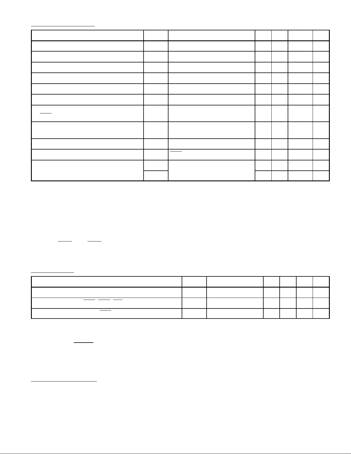
DC Characteristics: (TA = 0° to +70°C, VSS = 0V, VCC = +5V ±10% unless otherwise specified)
Parameter Symbol Test Conditions Min Typ Max Unit
Input High Voltage (All Inputs) V
Input Low Voltage (All Inputs) V
Output High Voltage V
Output Low Voltage V
Average VCC Supply Current I
Standby VCC Supply Current I
Average VCC Supply Current during
–only refresh cycles
RAS
Average VCC supply Current during
Page Mode
Input Leakage Current (Any Input) I
Output Leakage Current I
Supply Voltage V
I
I
V
CC1tRC
CC2
CC3
CC4
I (L)
O (L)
Notes 2, Note3 2.4 – VCC +1 V
IH
Notes 2, Note3 –1.0 – 0.8 V
IL
Note 4 2.4 – – V
OH
Note 5 – – 0.4 V
OL
= 260ns, Note 6 – – 70 mA
Note 7 – – 5 mA
Note 6 – – 65 mA
Note 6 – – 55 mA
– – 10 µA
CAS at Logic 1, 0 ≤ V out ≤ 5.5 – – 10 µA
Note 2 4.5 – 5.5 V
CC
SS
0 – 0 V
Note 2. All voltages referenced to VSS.
Note 3. Overshooting and undershooting on input levels of +6.5V or –2V for a period 0f 30ns Max.
will influence function and reliability of the device.
Note 4. I
Note 5. I
Note 6. I
= 4mA and 100pf load.
OH
= 4mA and 100pf load.
OL
depends on frequency of operation. Maximum current is measured at the fastest cycle
CC
rate.
Note 7. RAS
and CAS are both at VIH.
Capacitance:
Input Capacitance (A0–A8, DI) C
Input Capacitance (RAS, CAS, WE) C
Output Capacitance (DO, CAS = VIH to disable output) C
(Note 6)
Parameter Symbol Test Conditions Min Typ Max Unit
I1
I2
O
– – 6 pF
– – 7 pF
– – 7 pF
Note 6. Effective capacitance calculated from the equation:
C =
I • ∆t
with ∆V = 3V or measured with Boonton meter.
∆V
AC Test Conditions:
Input Pulse Levels 0 to 3.0V. . . . . . . . . . . . . . . . . . . . . . . . . . . . . . . . . . . . . . . . . . . . . . . . . . . . . . . . . . . . .
Input Rise and Fall Times 5ns between 0.8 and 2.4V. . . . . . . . . . . . . . . . . . . . . . . . . . . . . . . . . . . . . . .
Input Timing Reference Levels 0.8 to 2.4V. . . . . . . . . . . . . . . . . . . . . . . . . . . . . . . . . . . . . . . . . . . . . . . . .
Output Timing Reference Levels 0.4 to 2.4V. . . . . . . . . . . . . . . . . . . . . . . . . . . . . . . . . . . . . . . . . . . . . . .
Output Load equivelent to 2 standard TTL loads and 100pf. . . . . . . . . . . . . . . . . . . . . . . . . . . . . . . . . .
Page 4
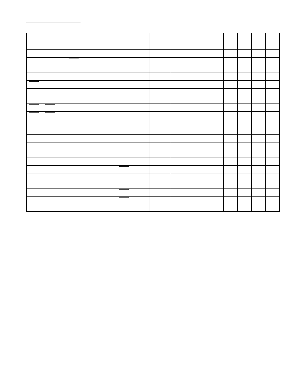
AC Characteristics: (TA = 0° to +70°C, VCC = 5V ±10%, Note 9, Note 10, Note 11 unless
otherwise specified)
Parameter Symbol Test Conditions Min Typ Max Unit
Random Read or Write Cycle Time t
Read–Modify–Write Cycle Time t
Access Time from RAS t
Access Time from CAS t
RAS Pulse Width t
CAS Pulse Width t
Refresh Period t
RAS Precharge Time t
CAS to RAS Precharge Time t
RAS to CAS Delay Time t
RAS Hold Time t
CAS Hold Time t
Row Address Setup Time t
Row Address Hold Time t
Column Address Setup Time t
Column Address Hold Time t
Column Address Hold Time referenced to RAS t
Transition Time (Rise and Fall) t
Read Command Setup Time t
Read Command Hold Time referenced to CAS t
Read Command Hold Time referenced to RAS t
Output Buffer Turn–Off Delay t
RC
RWC
RAC
CAC
RAS
CAS
REF
RP
CRP
RCD
RSH
CSH
ASR
RAH
ASC
CAH
AR
T
RCS
RCH
RRH
OFF
Note 12 260 – – ns
Note 12 310 – – ns
Notes 13, Note 14 – – 150 ns
Notes 13, Note 15 – – 75 ns
150 – 10
75 – – ns
– – 4 ms
100 – – ns
0 – – ns
Note 16 30 – 75 ns
75 – – ns
150 – – ns
0 – – ns
20 – – ns
0 – – ns
30 – – ns
Note 17 105 – – ns
Note 9 3 – 50 ns
0 – – ns
Note 18 0 – – ns
Note 18 10 – – ns
Note 19 0 – 40 ns
4
ns
Note 9. VIH and VIL are reference levels to measure timing of input signals. Also, transition times
are measured between V
and VIL.
IH
Note10. An i nit ial pa use o f 2 00µs is r equired after p ower–up followed b y a m inimum of e ight i nitialization
cycles prior to normal operation.
Note1 1. Th e time parame ter s s pe ci fie d h er e a re valid for a trans it ion time o f t
Note12. The specification for t
(Min), t
RC
(Min), and page–mode cycle time (tPC) are only used
RWC
= 5 ns for t he i nput signals
T
to indicate cycle time at which proper operation over full temperature range
(0°C ≤ T
≤ +70°C) is assured.
A
Note13. Measured with a load equivalent to two TTL loads and 100pf.
Note14. Assumes that t
shown in this table, t
Note15. Assumes that t
Note16. Operation within the t
cified as a reference point only. If t
access time is controlled exclusively by t
Note17. t
Note18. Either t
Note19. t
+ t
RCD
(Max) defines the time at which the output achieves the open circuit condition and is not
OFF
≥ tAR Min, t
CAH
or t
RRH
≤ t
RCD
≤ t
RCD
must be satisfied for a read cycle.
RCH
(Max). If t
RCD
will increase by the amount that t
RAC
(Max).
RCD
(Max) limit ensures that t
RCD
+ tDH ≥ t
RCD
is greater than the maximum recommended value
RCD
is greater than the specified t
RCD
CAC
Min, t
DHR
.
RCD
exceeds the value shown.
RCD
(Max) can be met. t
RAC
+ t
WCH
≥ t
WCR
Min.
(Max) is spe-
RCD
(Max) limit, then
RCD
referenced to output voltage levels.
Page 5
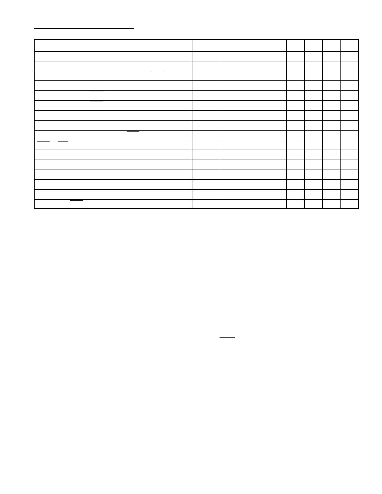
AC Characteristics (Cont’d): (TA = 0° to +70°C, VCC = 5V ±10%, Note 9, Note 10, Note 11
unless otherwise specified)
Parameter Symbol Test Conditions Min Typ Max Unit
Write Command Setup Time t
Write Command Hold Time t
Write Command Hold Time referenced to RAS t
Write Command Pulse Width t
Write Command to RAS Lead Time t
Write Command to CAS Lead Time t
Data in Setup Time t
Data in Hold Time t
Data in Hold Time referenced to RAS t
CAS to WE Delay t
RAS to WE Delay t
RMW Cycle RAS Pulse Width t
RMW Cycle CAS Pulse Width t
Page Mode Cycle Time t
Page Mode Read–Write Cycle Time t
Page Mode CAS Precharge Time t
WCS
WCH
WCR
WP
RWL
CWL
DHR
CWD
RWD
RRW
CRW
PRWC
Note 20 0 – – ns
45 – – ns
Note 17 120 – – ns
45 – – ns
45 – – ns
45 – – ns
Note 21 0 – – ns
DS
Note 21 45 – – ns
DH
Note 17 120 – – ns
Note 20 75 – – ns
Note 20 150 – – ns
200 – – ns
125 – – ns
Note 12 145 – – ns
PC
190 – – ns
CP
60 – – ns
Note 9. VIH and VIL are reference levels to measure timing of input signals. Also, transition times
are measured between V
and VIL.
IH
Note10. An i nit ial pa use o f 2 00µs is r equired after p ower–up followed b y a m inimum of e ight i nitialization
cycles prior to normal operation.
Note1 1. Th e time parame ter s s pe ci fie d h er e a re valid for a trans it ion time o f t
Note12. The specification for t
(Min), t
RC
(Min), and page–mode cycle time (tPC) are only used
RWC
= 5 ns for t he i nput signals
T
to indicate cycle time at which proper operation over full temperature range
Note17. t
Note20. t
(0°C ≤ T
RCD
WCS
sheet as electrical characteristics only: If t
≤ +70°C) is assured.
A
+ t
, t
≥ tAR Min, t
CAH
, and t
CWD
RWC
RCD
+ tDH ≥ t
DHR
Min, t
RCD
+ t
WCH
≥ t
WCR
Min.
are not restrictive operating parameters. They are included in the data
WCS
≥ t
(Min), the cycle is an early write cycle
WCS
and the Data Out will remain open circuit (high impedance) throughout the entire cycle; if
t
CWD
≥ t
(Min) and t
CWD
RWD
≥ t
(Min) the cycle is a read–write cycle and the Data Out
RWD
will cont a i n d a ta read from the selected cell. If neither of the above sets of conditions is satis-
fied, the condition of the Data Out (at access time) is indeterminate.
Note21. t
and tDH are referenced to the leading edge of CAS in early write cycles, and to the leading
DS
edge of WE in delayed write of read–modify–write cycles.
Page 6
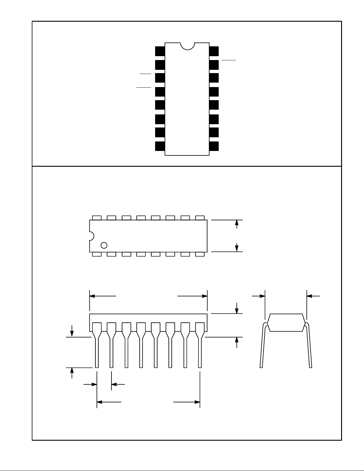
Pin Connection Diagram
1
A8
DI
2
A0
3
4
5
WE
RAS
6A2
A1
7
CC
8
V
16 9
V
16
CAS
15
DO
14
13
A6
12 A3
11
A4
10 A5
A7
9
SS
.245
(6.22)
Min
.260 (6.6) Max
18
.785 (19.9) Max
.300 (7.62)
.200 (5.08)
Max
.100 (2.54)
.700 (17.7)
 Loading...