

Page 1

NTE21128
Integrated Circuit
NMOS, 128K (16K x 8) UV EPROM
Description:
The NTE21128 is a 131,072 bit UV erasable and electrically programmable memory EPROM in a
28–Lead DIP type package organized as 16,384 words by 8 bits. The transparent lid allows the user
to expose the chip to ultraviolet light to erase the bit pattern. A new pattern can then be written to the
device by following the programming procedure.
Features:
D Access Time: 250ns
D Single 5V Supply Voltage
D Low Standby Current: 40mA Max
D TTL Compatible During Read and Program
D Fast Programming Algorithm
D Programming Voltage: 12V Typ
Absolute Maximum Ratings:
Supply Voltage, V
Program Supply, V
A9 Voltage, V
Input or Output Voltages, V
CC
PP
A9
IO
Ambient Operating Temperature, T
Temperature Under Bias, T
Storage Temperature Range, T
BIAS
stg
A
–0.6V to 6.25V. . . . . . . . . . . . . . . . . . . . . . . . . . . . . . . . . . . . . . . . . . . . . . . . . . . . . .
–0.6V to 14V. . . . . . . . . . . . . . . . . . . . . . . . . . . . . . . . . . . . . . . . . . . . . . . . . . . . . . .
–0.6V to 13.5V. . . . . . . . . . . . . . . . . . . . . . . . . . . . . . . . . . . . . . . . . . . . . . . . . . . . . . . . . .
–0.6V to 6.25V. . . . . . . . . . . . . . . . . . . . . . . . . . . . . . . . . . . . . . . . . . . . . .
0° to +70°C. . . . . . . . . . . . . . . . . . . . . . . . . . . . . . . . . . . . . . . . . . .
–10° to +80°C. . . . . . . . . . . . . . . . . . . . . . . . . . . . . . . . . . . . . . . . . . . . .
–65° to +125°C. . . . . . . . . . . . . . . . . . . . . . . . . . . . . . . . . . . . . . . . . .
Note 1. Except for the rating “Operating Temperature Range”, stresses above those listed in the
table “Absolute Maximum Ratings” may cause permanent damage to the device. These are
stress ratings only and operation of the device at these or any other conditions above those
indicated in the Operating sections of this specification is not implied. Exposure to Absolute
Maximum Rating conditions for extended periods may affect device reliability.
Page 2
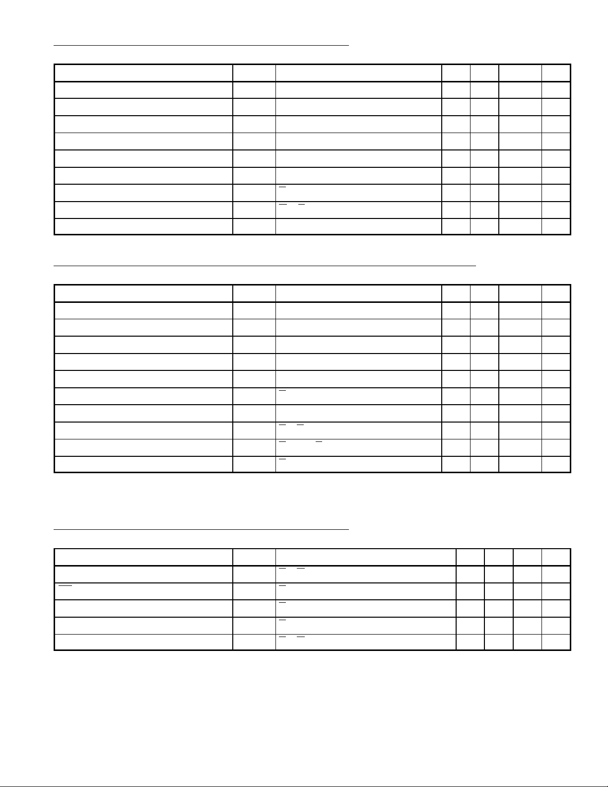
DC Characteristics (Read Mode and Standby Mode):
(TA = 0° to + 70°C, VCC = +5V ±5%, VPP = VCC)
Parameter Symbol Test Conditions Min Typ Max Unit
Output High Voltage V
Output Low Voltage V
Input High Voltage V
Input Low Voltage V
Output Leakage Current I
Input Leakage Current I
VCC Current (Standby) I
VCC Current (Active) I
VPP Current I
OHIOH
OLIOL
IH
IL
LO
LI
CC1
CC2
PP1
= –400µA 2.4 – – V
= 2.1mA – – 0.45 V
2.0 – VCC +1 V
–0.1 – 0.8 V
V
= 5.25V – – 10 µA
OUT
VIN = 5.25V – – 10 µA
E = V
IH
G = E = V
IL
– – 25 mA
– 60 100 mA
VPP = 5.25V – – 15 mA
DC Characteristics (Program, Program Verify, and Program Inhibit Modes):
(TA = +25°±5°C, VCC = +5V ±5% Note 2, VPP = +21V ±0.5V)
Parameter Symbol Test Conditions Min Typ Max Unit
Input High Voltage V
Input Low Voltage V
Input Leakage Current I
Output High Voltage V
Output Low Voltage V
VCC Current (Program Inhibit) I
VCC Current (Program Verify) I
VPP Current (Program) I
VPP Current (Program Verify) I
VPP Current (Program Inhibit) I
IH
IL
LI
OHIOH
OLIOL
CC1
CC2
PP2
PP3
PP4
VIN = VIL or V
= –400µA 2.4 – – V
IH
= 2.1mA – – 0.45 V
E = V
IH
E = P = V
E = VIL, P = V
E = V
IL
IH
IH
2.0 – VCC +1 V
–0.1 – 0.8 V
– – 10 µA
– – 25 mA
– – 100 mA
– – 30 mA
– – 15 mA
– – 15 mA
Note 2. VCC = 6V ±0.25V for high–speed programming.
AC Characteristics (Read Mode and Standby Mode):
(TA = 0° to + 70°C, VCC = +5V ±5%, VPP = VCC)
Parameter Symbol Test Conditions Min Typ Max Unit
Address to Output Delay t
CE to Output Delay t
Output Enable to Output Delay t
Output Enable High to Output Delay t
Address to Output Hold Time t
ACC
OE
OH
CE
DF
E = G = V
E = V
IL
E = V
IL
E = V
IL
E = G = V
IL
IL
Test Conditions:
Input Rise and Fall Times: 20ns
Input Pulse Levels: 0.45V to 2.4V
Timing Measurement Reference Levels:
Inputs: 0.8V and 2.0V
Outputs: 0.8V and 2.0V
– – 250 ns
– – 250 ns
– – 100 ns
0 – 85 ns
0 – – ns
Page 3

AC Characteristics (Program, Program Verify, and Program Inhibit Modes):
(TA = +25°±5°C, VCC = +5V ±5%, VPP = +21V ±0.5V)
Parameter Symbol Test Conditions Min Typ Max Unit
Address Setup Time t
E Setup Time t
Data Setup Time t
Address Hold Time t
E Setup Time t
Data Hold Time t
Chip Enable to Output Float Delay t
Data Valid from E t
Program Pulse Width (Note 3) t
VPP Setup Time t
OES
CES
PW
Input Pulse Levels = 0.45V to 2.4V,
AS
Input Timing Reference
Level = 0.8V and 2V,
Output Timing Reference
DS
Level = 0.8V and 2V,
Level = 0.8V and 2V,
Input Rise and Fall Times: 20ns
AH
DH
DF
OE
VS
Note 3. Initial Program Pulse width tolerance is 1msec ±5%.
Test Conditions:
Input Pulse Levels: 0.45V to 2.4V
Input Timing Reference Level: 0.8V and 2.0V
Output Timing Reference Level: 0.8V and 2.0V
Input Rise and Fall Times: 20ns
2 – – µs
2 – – µs
2 – – µs
0 – – µs
2 – – µs
2 – – µs
0 – 130 ns
– – 150 ns
45 50 55 ms
2 – – µs
Capacitance:
Input Capacitance C
Output Capacitance C
(TA = +25°C, f = 1MHz)
Parameter Symbol Test Conditions Min Typ Max Unit
VIN = 0V – 4 8 pF
IN
V
OUT
= 0V – 8 14 pF
OUT
Device Operation:
A single 5V power supply is required in the read mode. All inputs are TTL levels except for VPP.
Read Mode
The NTE21128 has the following two control functions: Chip Enable (E
device selection and Output Enable (G
) is the output control used to gate data to the output pins, inde-
) is the power control used for
pendent of device selection.
Address access time (t
) is equal to the delay from E to output (t
AVQV
outputs after the falling edge of G
for at least t
AVQV
– t
GLQV
.
, assuming that E has been low and the addresses have been stable
). Data is available at the
ELQV
Standby Mode
The standby mode, reducing the maximum active power current from 85mA to 40mA, is achieved by
applying a TTL high signal to the E
ance state, independent of the G
input. When in the standby mode, the outputs are in a high imped-
input.
Page 4

Device Operation (Cont’d):
Two Line Output Control
The NTE21128 features a 2 line control function which accommodates the use of multiple memory
connection. The two line control function allows:
a. the lowest possible memory power dissipation,
b. complete assurance that output bus contention will not occur.
For the most efficient use of these two control lines, E
device selecting function, while G
and connected to the READ
should be made a common connection to all devices in the array
line from the system control bus.
should be decoded and used as the primary
This ensures that all deselected memory devices are in their low power standby mode and that the
output pins are only active when data is required from a particular memory device.
System Considerations
The power switching characteristics of EPROMs require careful decoupling of the devices. The supply current (I
) has three segments that are of interest to the system designer: the standby current
CC
level, the active current level, and transient current peaks that are produced by the falling and rising
edges of E
. The magnitude of these transient current peaks is dependent on the capacitive and inductive loading of the device at the output. The associated transient voltage peaks can be suppressed
by complying with the two line output control and by properly selecting decoupling capacitors. It is
recommended that a 1µf ceramic capacitor be used on every device between V
and VSS. This
CC
should be a high frequency capacitor of low inherent inductance and should be placed as close to the
device as possible. In addition, a 4.7µf bulk electrolytic capacitor should be used between V
CC
and
GND for every eight devices. The bulk capacitor should be located near the power supply connection
point. The purpose of the bulk capacitor is to overcome the voltage drop caused by the inductive effects of PCB traces.
Programming
When delivered, all bits of the NTE21128 are in the “1” state. Data is introduced by selectively pro-
gramming “0s” into the desired bit locations. Although only “0s” will be programmed, both “1s” and
“0s” can be present in the data word. The only way to change a “0” to a “1” is by ultraviolet light erasure.
The NTE21128 is in the programming mode when the V
input is at 12.5V and E and P are at TTL
PP
low. The data to be programmed is applied 8 bits in parallel to the data output pins. The levels required
for the address and data inputs are TTL.
Fast Programming Algorithm
Fast Programming Algorithm rapidly programs the NTE21128 EPROM using an efficient and reliable
method suited to the production programming environment. Programming reliability is also ensured
as the incremental program margin of each byte is continually monitored to determine when it has
been successfully programmed. The Fast Programming Algorithm utilizes two different pulse types:
initial and overprogram.
The duration of the initial P
pulse(s) is 1ms, which will then be followed by a longer overprogram pulse
of length 3ms by n (n is equal to the number of the initial one–millisecond pulses applied to a particular
NTE21128 location), before a correct verify occurs. Up to 25 one–millisecond pulses per byte are
provided for before the over program pulse is applied.
The entire sequence of program pulses and byte verifications is performed at V
= 6V and VPP =
CC
12.5V. When the Fast Programming cycle has been completed, all bytes should be compared to the
original data with V
= 5V and VPP = 5V.
CC
Page 5

Device Operation (Cont’d):
Program Inhibit
Programming of multiple NTE21 128s in parallel with different data is also easily accomplished. Except for E
applied to a n NTE21128’s E
, all like inputs (including G) of the parallel NTE21128 may be common. A TTL low pulse
input, with VPP = 12.5V, will program that NTE21 128> A high level E input
inhibits the other NTE21128s from being programmed.
Program Verify
A verify should be performed on the programmed bits to determine that they were correctly programmed. The verify is accomplished with G
= VIL, E = VIL, P = VIH, and VPP at 12.5V.
Erasure Operation:
The erasure characteristic of the NTE21128 is such that erasure begins when the cells are exposed
to light with wavelengths shorter than approximately 4000 angstroms. The recommended erasure
procedure for the NTE21128 is exposure to short wave ultraviolet light which has a wavelength of
2537 angstroms. The integrated dose (i.e. UV intensity x exposure time) for erasure should be a minimum of 15 W sec/cm
an ultraviolet lamp with 12000 µW/cm
2
. The erasure time with this dosage is approximately 15 to 20 minutes using
2
power rating. The NTE21128 should be placed within 2.5cm
(1 inch) of the lamp tubes during the erasure. Some lamps have a filter on their tubes which should
be removed before erasure.
Pin Connection Diagram
V
A12
PP
A7
A6
A2
1
2
3
4
5A5
6A4
7A3
8
28
27
26
25
24
23
22
21
9A1 20
10A0
11
O0
12 17
O1
13
O2
19
18
16
14GND 15
V
CC
PGM
A13
A8
A9
A11
OE
A10
CE
O7
O6
O5
O4
O3
Page 6

1.449 (36.8)
28 15
.577
(14.6)
114
.230 (5.84) Max
.100 (2.54)
.100 (2.54) Min
 Loading...