

Page 1

NTE2055
Integrated Circuit
CMOS, 3 1/2 Digit A/D Converter
Description:
The NTE2055 is a high performance, low power, 3 1/2 digit A/D converter combining both linear CMOS and
digital CMOS circuits on a single monolithic IC. Available in a 24–Lead DIP type package, this device is designed to minimize use of external components. With two external resistors and two external capacitors, the
system forms a dual slope A/D converter with automatic zero correction and automatic polarity.
The NTE2055 is ratiometric and may be used over a full–scale range from 1.999V to 199.9mV. Systems using
this device may operate over a wide range of power supply voltages for ease of use with batteries, or with standard 5V supplies. The output drive conforms with standard B–Series CMOS specifications and can drive a
low–power Schottky TTL load.
The high impedance MOS inputs allow applications in current and resistance meters as well as voltmeters.
In addition to DVM/DPM applications, the NTE2055 finds use in digital thermometers, digital scales, remote
A/D, A/D control systems, and in MPU systems.
Features:
D Accuracy: ±0.05% of Reading ±1 Count
D Two Voltage Ranges: 1.999V and 199.9mV
D Up to 25 Conversions /s
D Z
D Auto–Polarity and Auto–Zero
D Single Positive Voltage Reference
D Standard B–Series CMOS Outputs: Drives One Low Power Schottky Load
D Uses On–Chip System Clock, or External Clock
D Wide Supply Range: e.g., ±4.5V to ±8.0V
D Overrange and Underrange Signals Available
D Operates in Auto Ranging Circuits
D Operates with LED and LCD Displays
D Low External Component Count
D Chip Complexity: 1326 FETs
> 100MΩ
in
Absolute Maximum Ratings:
DC Supply Voltage, VDD to V
EE
Voltage, Ant Pin, Referenced to V
DC Input Current, Per Pin, I
in
Operating Temperature Range, T
Storage Temperature Range, T
stg
, V –0.5V to VDD+0.5V. . . . . . . . . . . . . . . . . . . . . . . . . . . . . . . . . . . . . . . . . .
EE
A
–0.5V to +18V. . . . . . . . . . . . . . . . . . . . . . . . . . . . . . . . . . . . . . . . . . . . . . . . . . . .
±10mA. . . . . . . . . . . . . . . . . . . . . . . . . . . . . . . . . . . . . . . . . . . . . . . . . . . . . . . . . . . . .
–40° to +85°C. . . . . . . . . . . . . . . . . . . . . . . . . . . . . . . . . . . . . . . . . . . . . . . . . .
–65° to +150°C. . . . . . . . . . . . . . . . . . . . . . . . . . . . . . . . . . . . . . . . . . . . . . . . .
Note 1. Th is d evice contains circuitry to protect the inputs against damage due to high static voltages or electric
fields; however, it is advised that normal precautions be taken to avoid applications of any voltage higher
than maximum rated voltages to this high i mpedance circuit. For proper operation it i s recommended t hat
and V
V
in
Recommended Operating Conditions:
be constrained to the range VEE ≤ (Vin or V
out
(VSS = 0 or VEE)
) ≤ VDD.
out
DC Supply Voltage
to Analog GND, V
V
DD
to Analog GND, V
V
EE
Clock Frequency, f
Clk
DD
EE
Zero Offset Correction Capacitor, C
o
+5.0 to 8.0V. . . . . . . . . . . . . . . . . . . . . . . . . . . . . . . . . . . . . . . . . . . . . . . . . . . . .
–2.8 to –8.0V. . . . . . . . . . . . . . . . . . . . . . . . . . . . . . . . . . . . . . . . . . . . . . . . . . . .
32 to 400kHz. . . . . . . . . . . . . . . . . . . . . . . . . . . . . . . . . . . . . . . . . . . . . . . . . . . . . . . . . . . . . .
0.1 ±20%µF. . . . . . . . . . . . . . . . . . . . . . . . . . . . . . . . . . . . . . . . . . . . . . . . . .
Page 2
Electrical Characteristics: (CI = 0.1µF mylar, RI = 470kΩ @ V
= 300kΩ, TA = +25°C ; all voltages referenced to Analog GND, Pin1, unless
R
C
= 2V, RI = 27kΩ @ V
ref
= 200mV,
ref
otherwise specified)
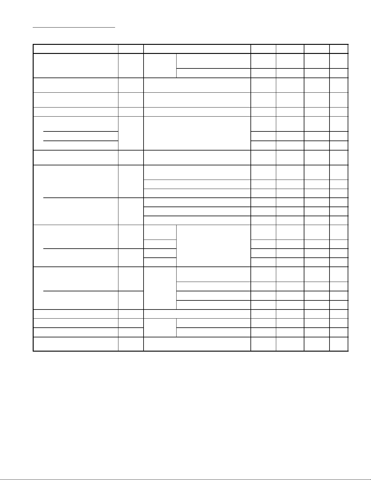
Parameter Symbol Test Conditions Min Typ Max Unit
V
Linearity–Output Reading VDD = 5V,
V
= –5V,
EE
Note 2
Stability – Output Reading VDD = 5V, VEE = –5V, VX = 199mV,
V
= 200mV
ref
Symmetry – Output Reading VDD = 5V, VEE = –5V, V
Note 3
Zero–Output Reading VDD = 5V, VEE = –5V, VX = 0V, V
= 2.000V –0.05
ref
V
= 200.0mV – ±0.05 – %rdg
ref
– Count
– – 3 LSD
= 2000mV,
ref
= 2V – 0 0 LSD
ref
– – 4 LSD
Bias Current
Analog Input
VDD = 5V, VEE = –5V
– ±20 ±100 pA
Reference Input – ±20 ±100 pA
Analog GND – ±20 ±500 pA
Common Mode Rejection VDD = 5V, VEE = –5V, f
VX = 1.4V, V
ref
= 2V
= 32kHz,
Clk
– 65 – dB
Input Voltage (Pin9, Pin10)
“0” Level V
VDD = 5V, VO = 4.5V or 0.5V, Note 3 – 2.25 1.5 V
IL
VDD = 10V, VO = 9V or 1V, Note 3 – 4.50 3.0 V
VDD = 15V, VO = 13.5V or 1.5V, Note 3 – 6.75 4.0 V
“1” Level V
VDD = 5V, VO = 0.5V or 4.5V, Note 3 3.5 2.75 – V
IH
VDD = 10V, VO = 1V or 9V, Note 3 7.0 5.50 – V
VDD = 15V, VO = 1.5V or 13.5V, Note 3 11.0 8.25 – V
Output Voltage (Pin14 to Pin23)
“0” Level V
VSS = 0V VDD = 5V, VEE = –5V – 0 0.05 V
OL
VSS = –5V – –5.0 –4.95 V
“1” Level V
VSS = 0V 4.95 –5.0 – V
OH
VSS = –5V 4.95 5.0 – V
Output Current (Pin14 to Pin23)
Source I
Sink I
OH
OL
VDD = 5V,
VEE = –5V
VSS = 0V, VOH = 4.6V –0.2 –0.36 – mA
VSS = –5V, VOH = 4.5V –0.5 –0.9 – mA
VSS = 0V, VOL = 0.4V 0.51 0.88 – mA
VSS = –5V, VOL = –4.5V 1.3 2.25 – mA
Input Current (DU, Pin9) I
Quiescent Current I
DC Supply Rejection VDD = 5V, VEE = –5V, VDD to VEE, ISS = 0,
VDD = 5V, VEE = –5V – ±0.00001 ±0.3 µA
DU
Q
VDD to VEE,
ISS = 0
VDD = 5V, VEE = –5V – 0.9 2.0 mA
VDD = 8V, VEE = –8V – 1.8 4.0 mA
– 0.5 – mV/V
V
= 2V
ref
±0.05 +0.05
+ Count
%rdg
Note 2. Accuracy – The accuracy of the meter at full scale is the accuracy of the setting of the reference volt-
age. Zero is recalculated during each conversion cycle. The meaningful specification is linearity.
In other words, the deviation from correct reading for all inputs other than positive full scale and zero
is defined as the linearity specification.
Note 3. Symmetry – Defined as the difference between a negative and positive reading of the same voltage
at or near full scale.
Note 4. Referenced to V
for Pin9. Referenced to VEE for Pin10.
SS
Page 3

Truth Table
Coded Condition
of MSD Q3 Q2 Q1 Q0
+0 1 1 1 0 Blank
–0 1 0 1 0 Blank
+0 UR 1 1 1 1 Blank
–0 UR 1 0 1 1 Blank
(DS1 =1)
BCD to 7 Segment
Decoding
+1 0 1 0 0 4 → 1
–1 0 0 0 0 0 → 1
+1 OR 0 1 1 1 7 → 1
–1 OR 0 0 1 1 3 → 1
Hook up
only seg b
and c to
MSD
Notes for Truth Table:
Q3 –1/2 digit, low for “1”, high for “0”
Q2 – Polarity: “1” = positive, “0” = negative
Q0 – Out of range condition exists if Q0 =1. When used in conjunction with Q3 the type
of out of range condition is indicated, i.e., Q3 = 0 → OR or Q3 = 1 → UR.
When only segment b and c of the decoder are connected to the
1
/2 digit of the display 4,
0, 7, and 3 appear as 1.
The overrange indication (Q3 = 0 and Q0 = 1) occurs when the count is greater than 1999,
e.g., 1.999V for a reference of 2V. The underrage indication, useful for autoranging circuits,
occurs when the count is less than 180, e.g., o.180V for a reference of 2V.
Caution: If the most significant digit is connected to a display other than a “1” only; such as
a full digit display, segments other than b and c must be disconnected. The BCD
ti seven decoder must blank on BCD inputs 1010 to 1111.
Pin Connection Diagram
V
1
AG
V
2
ref
V
3
X
R
4
I
RI/C
5
I
C
6
I
CO 1
7
CO 2
8 17
DU DS 49 16
CLK 1 10 15
CLK 2 EOC
11 14
V
12 13
EE
V
24
DD
23
Q2
22
21Q3Q1
20
Q0
19 DS 1
18 DS 2
DS 3
OR
V
SS
Page 4

24 13
112
1.300 (33.02)
Max
.100 (2.54)
1.100 (27.94)
.225
(5.73)
Max
.126
(3.22)
Min
.520
(13.2)
.600
(15.24)
 Loading...