

Page 1

NTE2050 & NTE2051
Integrated Circuit
31/2–Digit Single Chip A/D Converter
Description:
The NTE2050 and NTE2051 are high performance, low power 3–1/2 digit A/D converters containing
all the necessary active devices on a single CMOS IC. Included are seven segment decoders, display
drivers, reference and a clock. The NTE2051 is designed to interface with a liquid crystal display
(LCD) and includes a backplane drive; the NTE2050 will directly drive an instrument–size light emitting diode (LED) display.
The NTE2050 and NTE2051 bring together an unprecedented combination of high accuracy, versatility, and true economy. High accuracy like auto–zero to less than 10µV, zero drift of less than 1µV/°C,
input bias current of 10pA max., and roll–over error of less than one count. The versatility of true differential input and reference is useful in all systems, but gives the designer an uncommon advantage
when measuring load cells, strain gauges and other bridge–type transducers. And, finally, the true
economy of single power supply operation (NTE2051), enabling a high performance panel meter to
be built with the addition of only 7 passive components and a display.
Features:
D Guaranteed Zero Reading for 0 Volts Input on all Scales
D True Polarity at Zero for Precise Null Detection
D Input Current: 1pA Typ
D True Differential Input and Reference
D Direct Display Drive – No External Components Required:
NTE2050 (LED)
NTE2051 (LCD)
D Low Noise – Less than 15µV
D On–Chip Clock and Reference
D Low Power Dissipation – Typically Less than 10mW
D No Additional Active Circuits Required
P–P
Page 2
Absolute Maximum Ratings:
Supply Voltage,
NTE2051, V+ to V– 15V. . . . . . . . . . . . . . . . . . . . . . . . . . . . . . . . . . . . . . . . . . . . . . . . . . . . . . . . . . .
NTE2050, V+ to GND +6V. . . . . . . . . . . . . . . . . . . . . . . . . . . . . . . . . . . . . . . . . . . . . . . . . . . . . . . . .
NTE2050, V– to GND –9V. . . . . . . . . . . . . . . . . . . . . . . . . . . . . . . . . . . . . . . . . . . . . . . . . . . . . . . . .
Analog Input Voltage (Either Input, Note 2) V+ to V–. . . . . . . . . . . . . . . . . . . . . . . . . . . . . . . . . . . . . . . .
Reference Input Voltage (Either Input) V+ to V–. . . . . . . . . . . . . . . . . . . . . . . . . . . . . . . . . . . . . . . . . . . .
Clock Input,
NTE2051 TEST to V+. . . . . . . . . . . . . . . . . . . . . . . . . . . . . . . . . . . . . . . . . . . . . . . . . . . . . . . . . . . . .
NTE2050 GND to V+. . . . . . . . . . . . . . . . . . . . . . . . . . . . . . . . . . . . . . . . . . . . . . . . . . . . . . . . . . . . . .
Power Dissipation (Note 3) 800mW. . . . . . . . . . . . . . . . . . . . . . . . . . . . . . . . . . . . . . . . . . . . . . . . . . . . . . .
Operating Temperature Range 0° to +70°C. . . . . . . . . . . . . . . . . . . . . . . . . . . . . . . . . . . . . . . . . . . . . . . .
Storage Temperature Range –65° to +160°C. . . . . . . . . . . . . . . . . . . . . . . . . . . . . . . . . . . . . . . . . . . . . . .
Lead Temperature (During Soldering, 60sec) +300°C. . . . . . . . . . . . . . . . . . . . . . . . . . . . . . . . . . . . . . .
Note 1. Stresses above those listed under “Absolute Maximum Ratings” may cause permanent
damage to the device. These are stress ratings only, and functional operation of the device
at these or another conditions above those indicated in the operational section of the specification is not implied. Exposure to absolute maximum rating conditions for extended periods
may affect device reliability.
Note 2. Input v oltages m ay e xceed t he s upply voltages p rov ided t he i nput c urr ent is l im ited t o ±100µA.
Note 3. Dissipation rating assumes device is mounted with all leads soldered to printed circuit board.
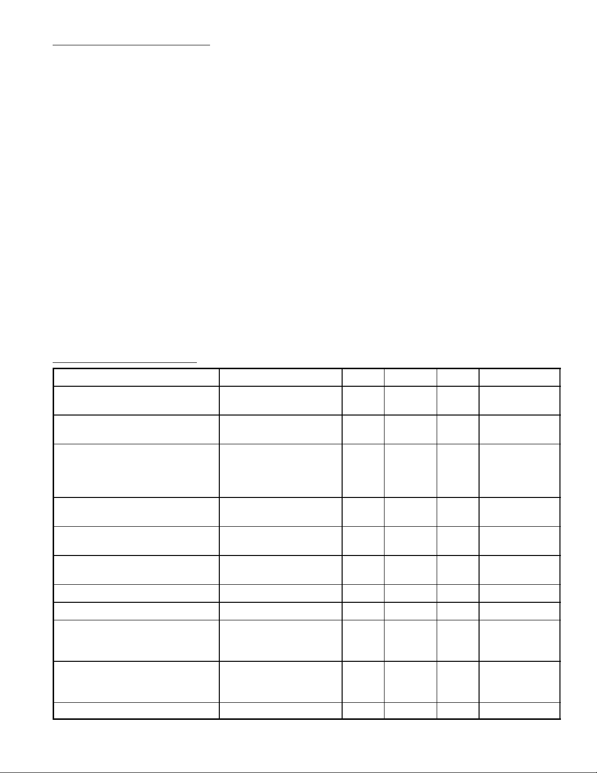
Electrical Characteristics: (TA = +25°C, f
Parameter Test Conditions Min Typ Max Unit
Zero Input Reading VIN = 0V
Full Scale = 200mV
Ratiometric Reading VIN = V
V
Rollover Error (Difference in
Reading for Equal Positive and
Negative Reading near Full
Scale)
Linearity (Maximum Deviation
from Best Straight Line Fit)
Common Mode Rejection Ratio VCM = ±1V, VIN = 0V
Noise (Peak–Peak Value not
Exceeded 95% of Time)
Leakage Current | Input VIN = 0 – 1 10 pA
Zero Reading Drift VIN = 0, 0° < TA < +70°C – 0.2 1.0 µV/°C
Scale Factor Temperature
Coefficient
–VIN = +VIN ] 200mV –1 ±.2 +1 Counts
Full Scale = 200mV
or Full Scale = 2V
Full Scale = 200mV
VIN = 0V
Full Scale = 200mV
VIN = 199.0mV
0° < T
(Ext. Ref. 0ppm/°C)
= 100mV
REF
A
REF
< +70°C
= 48kHz unless otherwise specified)
clock
–000.0 ±000.0 +000.0 Digital Reading
999 999/1000 1000 Digital Reading
–1 ±.2 +1 Counts
– 50 – µV/V
– 15 – µV
– 1 5 ppm/°C
V+ Supply Current (Does Not
Include LED Current for
NTE2050)
V– S upply C urrent (NTE2050 O nly) – 0.6 1.8 mA
VIN = 0 – 0.8 1.8 mA
Page 3

Electrical Characteristics (Cont’d): (TA = +25°C, f
Parameter Test Conditions Min Typ Max Unit
= 48kHz unless otherwise specified)
clock
Analog Common Voltage Common
(With Respect to Positive Supply)
Temperature Coef ficient of A nalog
Common (With Respect to
25kΩ Between Com m on
& Positive Supply
25kΩ Between Com m on
& Positive Supply
2.4 2.8 3.2 V
– 80 – ppm/°C
Positive Supply)
Peak–Peak S egment Drive V oltage,
V+ to V– = 9V, Note 4 4 5 6 V
Peak–Peak Backplane Drive
Voltage (NTE2051 Only)
Segment Sinking Current
(NTE2050 Only)
(Except Pin19)
(Pin19 Only)
V+ = 5V
Segment Voltage = 3V
5
10
8
16
–
–
mA
Note 4. Back plane drive is in phase with segment drive for “off” segment, 180° outp of phase for “on”
segment. Frequency is 20 times conversion rate. Average DC component is less than
50mV.
Pin Connection Diagram
Units V(+)
Units D1
Units C1
1
2
3
40
39
38
OSC 1
OSC 2
OSC 3
Units B1
Units A1
Units F1
Units G1
Units E1
Tens D2 Common
Tens C2
Tens B2 In Low
T ens A2
Tens F2
Tens E2
100’s D3
100’s B3
100’s F3 C3 100’s
100’s E3
Polarity (–)
4
5
6
7
8 33
9 32
10 31 In High
11 30
12 29
13
14
15
16 25
17 24
18 23 A3 100’s
19 22
AB4 G3 100’s
20 21
37
Test
36
Ref High
35 Ref Low
34 C (+) Ref
C (–)
A/Z
28
Buff
27 Int
26 V (–)
G2 Tens
BP/GND*
Note: Pin21 is GND on the NTE2050
Page 4

40 21
1
2.055 (52.2)
.100 (2.54) .019 (0.5)
20
.155 (3.9)
.137
(3.5)
.550 (13.9)
Max
.650 (16.5)
 Loading...