

Page 1
NTE1639
Integrated Circuit
CMOS Clock Generator/Driver for BBDs
Description:
The NTE1639 is a CMOS LSI Clock Generator ina 8–Lead DIP type package capable of generating
two phase clock signals of low output impedance for use as a BBD driver. The built–in V
supply circuit provides the proper voltages needed for driving BBDs such as the NTE1641.
Features:
D BBD Direct Driving Capability of up to two BBD’s
D Self and Separate Oscillations.
D Two Phase Clock Output (Duty: 1/2)
D Built–in V
Voltage Generator for Driving the NTE1641 BBD.
GG
D Single Power Supply: –8V to –16V.
Applications:
D BBD Clock Generator/Driver.
GG
power
Absolute Maximum Ratings:
Drain Supply Voltage, V
DD
Input/Output Pin Voltage, V
Power Dissipation, P
D
(TA = +25°C unless otherwise specified)
I, VO
Operating Ambient Temperature Range, T
Storage Temperature Range, T
stg
Recommended Operating Conditions:
Item
Drain Supply Voltage V
Symbol Condition Min Typ Max Unit
DD
GND = 0V –8 –15 –16 V
VDD –0.3V to +0.3V. . . . . . . . . . . . . . . . . . . . . . . . . . . . . . . . . . . . . . . .
opr
(TA = +25°C unless otherwise specified)
–18V to +0.3V. . . . . . . . . . . . . . . . . . . . . . . . . . . . . . . . . . . . . . . . . . . . . . . . . .
200mW. . . . . . . . . . . . . . . . . . . . . . . . . . . . . . . . . . . . . . . . . . . . . . . . . . . . . . . . . .
–10° to +70°C. . . . . . . . . . . . . . . . . . . . . . . . . . . . . . . . . .
–30° to +125°C. . . . . . . . . . . . . . . . . . . . . . . . . . . . . . . . . . . . . . . . . .
Page 2
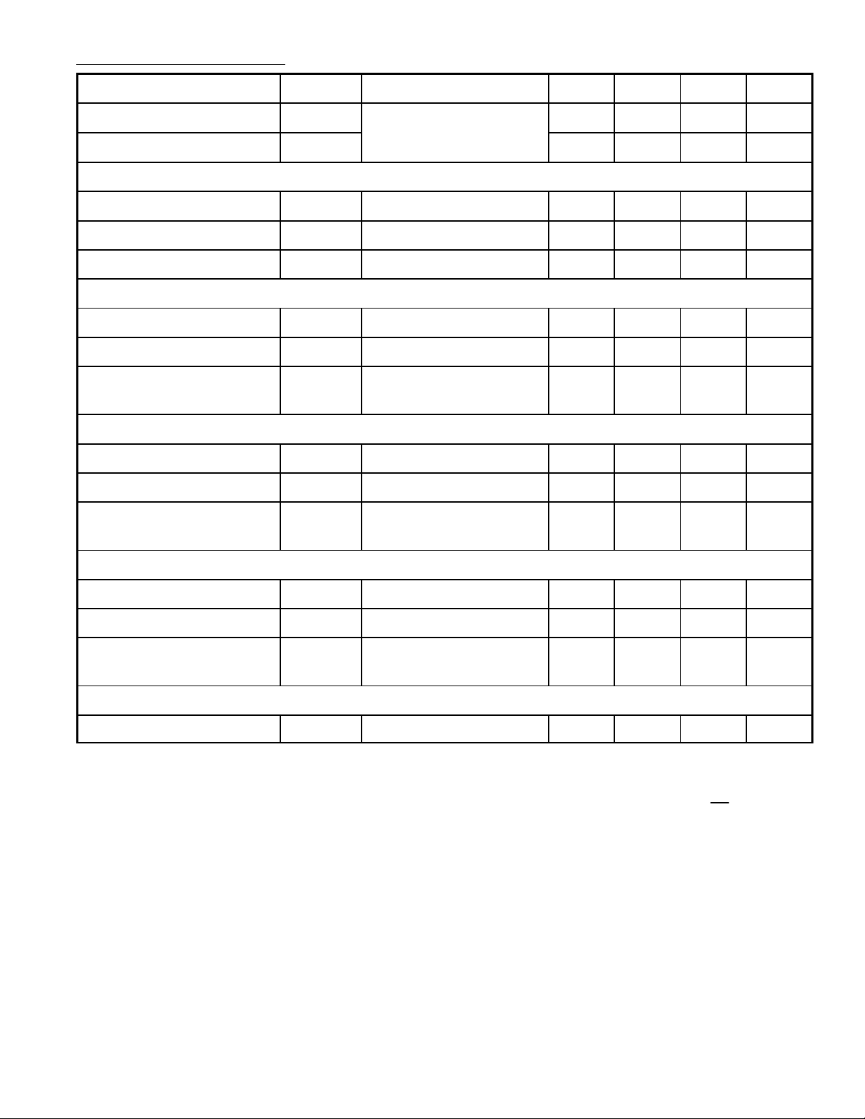
Electrical Characteristics: (TA = +25°C, VDD = –15V, GND = 0V unless otherwise specified)
Parameter
Symbol Test Condition Min Typ Max Unit
Input Drain Current I
Total Power Dissipation P
OX1 Input Pin
Voltage “H” Level V
Voltage “L” Level V
Input Leakage Current I
Leak
OX2 Output Pin
Output Current “H” Level I
Output Current “L” Level I
Output Leakage Current I
OH(1)
OL(1)
LOL(1)
OX3 Output pin
Output Current “H” Level I
Output Current “L” Level I
OH(2)
OL(2)
DD
tot
IH
IL
No load
No load
Clock Output 40kH
Z
– 3 – mA
– 45 – mW
0 – –1 V
VDD+1 – V
DD
V
VI = 0V to –15V – – 30 µA
VO = –1V 0.6 – – mA
VO = –14V 0.5 – – mA
VO = V
DD
VO = GND
–
–
–
–
30
30
µA
µA
VO = –1V 1.5 – – mA
VO = –14V 2 – – mA
Output Leakage Current I
LOL(2)
VO = V
DD
VO = GND
CP1, CP2 output pin
Output Current “H” Level I
Output Current “L” Level I
Output Leakage Current I
OH(3)
OL(3)
LOL(3)
VO = –1V 10 – – mA
VO = –14V 10 – – mA
VO = V
DD
VO = GND
VGG OUT output pin (Note 1)
Output Voltage V
GG(Out)
Note 1. This pin generates the VGG voltage for a BBD manufac-
tured by NTE. So therefore, it might not be applicable for
other devices. In any case, the V
GG(OUT)
changes by the
following formula depending on the value of VDD.
–
–
–
–
–
–
–
–
30
30
30
30
–14 V
14
V
GG(OUT)
≅
15
V
µA
µA
µA
µA
DD
Page 3

Pin Descriptions:
Pin No. Symbol Pin Name Description
1 GND Ground Connected to GND of the circuit.
2 CP1 Clock Output 1 This pin outputs a clock signal that is the reverse
phase of CP2 with a Duty Cycle of 1/2 the frequency
of oscillation.
3 V
DD
VDD apply –15V is applied
4 CP2 Clock Output 2 This pin outputs a clock signal that is a the reverse
phase of CP1
5 OX3
6 OX2
7 OX1
8 V
GG OUT
OSC connections to R, C are connected for the In case of separate excita-
C1, R2, and R
separately
separately opened and OX1 is set to
1
internal clock. tion, OX3 and OX2 are
opened and OX1 is set to
OSC input.
VGG Voltage Output –14V is output. (VDD = –15V) V
GG OUT
= 14/15VDD.
The Maximum Clock Frequency:
The upper limit value of the clock frequency is determined by the load capacitance and power consumption. The maximum power dissipation for the NTE1639 is P
= 200mW . If the clock frequency
D
of the load capacitance is increased, the power consumption will be increased. Accordingly , in order
to utilize this device with a dissipation less than the permissible value, it is necessary to select adequate values for the clock frequency and load capacitance. By connecting a resistance to the clock
output pin, it is possible to increase the value of the maximum clock frequency without increasing dissipation. Because the dissipation on the LSI side is lessened, part of the power consumption required
for driving the load capacitance is consumed by the series resistance.
Pin Connection Diagram
GND
CP 1
CP 2
1
2
V
3
DD
4
8
7
6
5
V
GG
OX 1
OX 2
OX 3
(Out)
Page 4

85
.256 (6.52) Max
14
.393 (10.0)
Max
.300 (7.62)
.300
(7.62)
.150
(3.81)
.070 (1.77) Min.100 (2.54)
 Loading...