

Page 1

NTE1641
Integrated Circuit
1024 Stage BBD for Audio Signal Delays
Description:
The NTE1641 is a 1024–stage long delay low noise BBD that provides a signal delay of up to
51.2msec. This device is suitable for use as the reverberation effect of an electronic musical instrument, or in stereo equipment, due to its long delay times.
Features:
D Variable delay time of audio signal: 5.12ms to 51.2ms.
D Clock component cancellation capability.
D No insertion loss: L
D Wide dynamic range: S/N ≅ 80dB typ.
D Wide frequency response: f
D Low distortion: THD = 0.5% typ. (V
D Clock frequency range: 10 to 100kH
D P channel silicon gate process.
D 8–Lead DIP plastic package.
= 0dB typ.
i
≤ 12kHZ.
i
= 0.78V
i
.
Z
rms
)
Applications:
D Reverberation effect echo for P.A. and stereo equipment.
D Chorus effect in electronic musical instruments.
D Variable or fixed delay of analog signals
D Telephone time compression and delay line for voice communication systems, etc.
Absolute Maximum Ratings:
Pin Voltage, V
Output Voltage, V
, VGG, VCP, V
DD
O
Operating Ambient Temperature Range, T
Storage Temperature Range, T
(TA = +25°C unless otherwise specified)
I
opr
stg
–18V to +0.3V. . . . . . . . . . . . . . . . . . . . . . . . . . . . . . . . . . . . . . . . . . . .
–18V to +0.3V. . . . . . . . . . . . . . . . . . . . . . . . . . . . . . . . . . . . . . . . . . . . . . . . . . . . . .
–20° to +60°C. . . . . . . . . . . . . . . . . . . . . . . . . . . . . . . . .
–55° to +125°C. . . . . . . . . . . . . . . . . . . . . . . . . . . . . . . . . . . . . . . .
Page 2
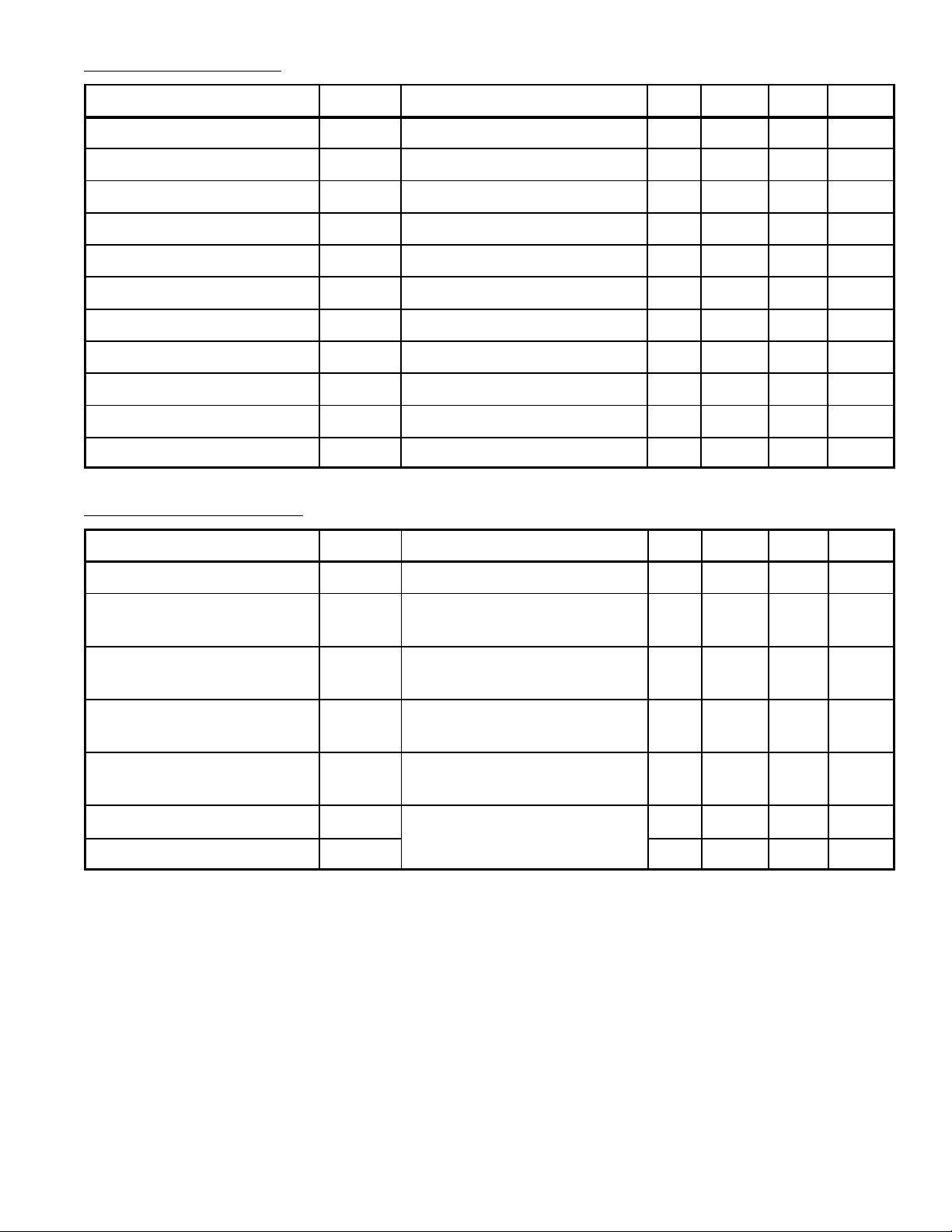
Operating Conditions: (TA = +25°C unless otherwise specified)
Parameter
Drain Supply Voltage V
Gate Supply Voltage V
Clock Voltage “H” Level V
Clock Voltage “L” Level V
Clock Frequency f
Clock Pulse Width t
Clock Rise Time t
Clock Fall Time t
Clock Input Capacitance C
Clock Cross Point V
Input DC Bias Voltage V
Symbol Condition Min Typ Max Unit
DD
GG
CPH
CPL
CP
2
W(CP)
2
r(CP)
2
f(CP)
CP
2
X
Bias
Electrical Characteristics: (TA = +25°C, VDD = V
Parameter
Symbol Condition Min Typ Max Unit
= –15V, V
CPL
–14 –15 –16 V
– VDD+1 – V
0 – –1 V
– V
DD
– V
10 – 100 kH
1
0.5T
– – 500 µs
– – 500 ns
– – 700 V
0 – –3 V
–5 – –10 V
= 0V, VGG = –14V, RL = 100kΩ)
CPH
Z
–
Signal Delay Time t
Input Singal Frequency f
D
i
fCP = 40kHz, Vi = 1.5Vrms,
3dB down (0dB at f
= 1kHZ)
i
Input Voltage Amplitude υi fCP = 40kHZ, fi = 1kHZ,
THD = 2.5%
Insertion Loss Li fCP = 40kHZ, fi = 1kHZ,
V
= 1.5V
i
rms
Total Harmonic Distortion THD fCP = 40kHZ, fi = 1kHZ,
V
= 0.78V
Output Noise Voltage V
no
i
fCP = 100kHZ,
rms
Weighted by “A” curve
Signal to noise ratio S/N
Note 1. T = 1/fcp (Clock Period)
Note 2. Clock pulse waveforms
5.12 – 51.2 ms
12 – – kH
1.5 – – V
rms
–4 0 4 dB
– 0.5 2.5 %
– – 0.3 mV
– 80 – dB
Z
rms
Page 3
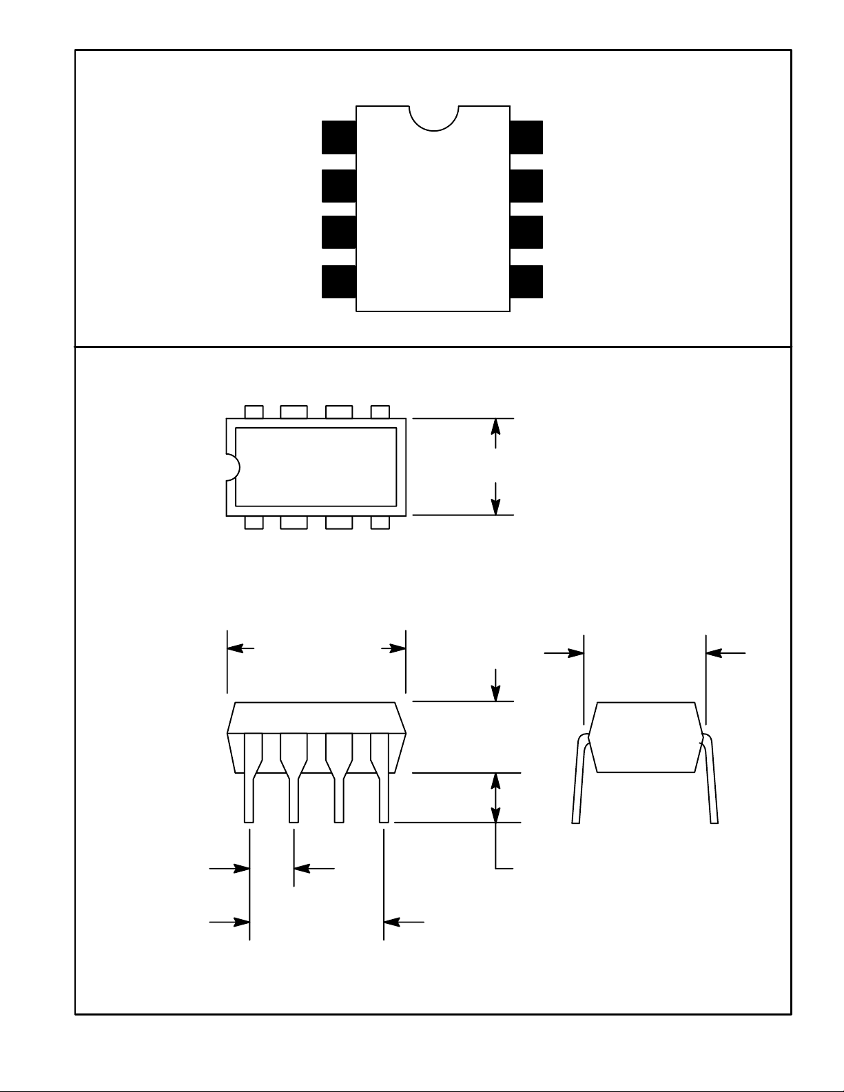
Pin Connection Diagram
GND
CP 1
Input
V
GG
1
2
3
4
85
.256 (6.52) Max
8
7
6
5
Output 2
Output 1
CP 2
V
DD
14
.393 (10.0)
Max
.150
(3.81)
.300 (7.62)
.300
(7.62)
.070 (1.77) Min.100 (2.54)
 Loading...