

Page 1
查询NJL0281D供应商
NL27WZ00
Dual 2−Input NAND Gate
The NL27WZ00 is a high performance dual 2−input NAND Gate
operating from a 1.65 V to 5.5 V supply.
• Extremely High Speed: t
• Designed for 1.65 V to 5.5 V V
• Over Voltage Tolerant Inputs
• LVTTL Compatible − Interface Capability With 5 V TTL Logic with
= 3 V
V
CC
• LVCMOS Compatible
• 24 mA Balanced Output Sink and Source Capability
• Near Zero Static Supply Current Substantially Reduces System
Power Requirements
• Replacement for NC7WZ00
• Chip Complexity: FET = 112
2.4 ns (typical) at VCC = 5 V
PD
Operation
CC
http://onsemi.com
8
1
US8
US SUFFIX
CASE 493
MARKING
DIAGRAM
8
D
L1
1
A1
B1
Y2
GND
D = Date Code
8
1
2
3
4
V
CC
Y1
7
See detailed ordering and shipping information in the package
dimensions section on page 4 of this data sheet.
6
B2
5
A2
ORDERING INFORMATION
IEEE/IEC
A1
B1
A2
B2
&
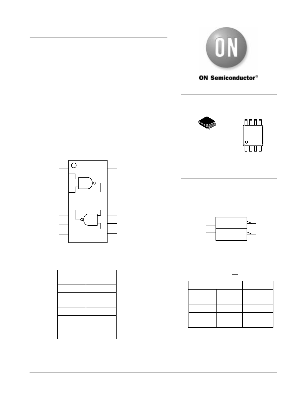
Figure 1. Pinout Figure 2. Logic Symbol
PIN ASSIGNMENT
FUNCTION TABLE
Pin
1
2
3
4
5
6
7
8
Function
A1
B1
Y2
GND
A2
B2
Y1
V
CC
Y = AB
Inputs
A
L
L
H
H
H = HIGH Logic Level
L = LOW Logic Level
B
L
H
L
H
Y1
Y2
Output
Y
H
H
H
L
Semiconductor Components Industries, LLC, 2003
November, 2003 − Rev. 4
1 Publication Order Number:
NL27WZ00/D
Page 2

Page 3

Page 4

NL27WZ00
tf = 3 ns
INPUT
A and B
OUTPUT Y
90%
90%
t
PHL
50%
10%
50%
50%
50%
Figure 3. Switching Waveform
t
PLH
10%
= 3 ns
t
f
V
CC
GND
V
OH
V
OL
V
CC
INPUT
CL*
includes all probe and jig capacitances.
*C
L
A 1−MHz square input wave is recommended
for propagation delay tests.
Figure 4. Test Circuit
OUTPUT
DEVICE ORDERING INFORMATION
Device Nomenclature
Device Order
Number
Logic Circuit
Indicator
NL27WZ00US NL 2 7 WZ 00 US US8 178 mm, 3000
†For information on tape and reel specifications, including part orientation and tape sizes, please refer to our Tape and Reel Packaging
Specifications Brochure, BRD8011/D.
No. of Gates
per Package
Temp Range
Identifier
Technology
Device
Function
Package
Suffix
Package
Type
Tape and
Reel Size
Unit
†
http://onsemi.com
4
Page 5

NL27WZ00
CAVITY
TAPE
TOP TAPE
TAPE DIMENSIONS mm
8.00
+ 0.30
− 0.10
TAPE TRAILER
(Connected to Reel Hub)
NO COMPONENTS
160 mm MIN
Figure 5. Tape Ends for Finished Goods
4.00
2.00
4.00
COMPONENTS
DIRECTION OF FEED
TAPE LEADER
NO COMPONENTS
400 mm MIN
1.50 TYP
1.75
3.50 0.25
1
1.00 ± 0.25 TYP
DIRECTION OF FEED
Figure 6. US8 Reel Configuration/Orientation
http://onsemi.com
5
Page 6

NL27WZ00
1.5 mm MIN
(0.06 in)
(0.512 in 0.008 in)
t MAX
13.0 mm 0.2 mm
20.2 mm MIN
A
(0.795 in)
REEL DIMENSIONS
Tape Size
8 mm
T and R Suffix
FULL RADIUS
Figure 7. Reel Dimensions
A Max
US
178 mm
(7 in)
DIRECTION OF FEED
G
8.4 mm, + 1.5 mm, −0.0
(0.33 in + 0.059 in, −0.00)
50 mm MIN
(1.969 in)
G
t Max
14.4 mm
(0.56 in)
BARCODE LABEL
Figure 8. Reel Winding Direction
http://onsemi.com
6
HOLEPOCKET
Page 7

−T−
SEATING
PLANE
A
58
P
D
G
K
0.10 (0.004) XY
M
41
−X−
LB
T
−Y−
C
NL27WZ00
PACKAGE DIMENSIONS
US8
US SUFFIX
CASE 493−02
ISSUE A
J
DETAIL E
R
S
U
T0.10 (0.004)
V
DETAIL E
H
N
F
NOTES:
R 0.10 TYP
M
1. DIMENSIONING AND TOLERANCING PER
ANSI Y14.5M, 1982.
2. CONTROLLING DIMENSION: MILLIMETERS.
3. DIMENSION “A” DOES NOT INCLUDE MOLD
FLASH, PROTRUSION OR GATE BURR.
MOLD FLASH. PROTRUSION AND GATE
BURR SHALL NOT EXCEED 0.140 MM
(0.0055”) PER SIDE.
4. DIMENSION “B” DOES NOT INCLUDE
INTER−LEAD FLASH OR PROTRUSION.
INTER−LEAD FLASH AND PROTRUSION
SHALL NOT E3XCEED 0.140 (0.0055”) PER
SIDE.
5. LEAD FINISH IS SOLDER PLATING WITH
THICKNESS OF 0.0076−0.0203 MM.
(300−800 “).
6. ALL TOLERANCE UNLESS OTHERWISE
SPECIFIED ±0.0508 (0.0002 “).
MILLIMETERS
DIMAMIN MAX MIN MAX
1.90 2.10 0.075 0.083
B 2.20 2.40 0.087 0.094
C 0.60 0.90 0.024 0.035
D 0.17 0.25 0.007 0.010
F 0.20 0.35 0.008 0.014
G 0.50 BSC 0.020 BSC
H 0.40 REF 0.016 REF
J 0.10 0.18 0.004 0.007
K 0.00 0.10 0.000 0.004
L 3.00 3.20 0.118 0.126
M 0 6 0 6
N 5 10 5 10
P 0.23 0.34 0.010 0.013
R 0.23 0.33 0.009 0.013
S 0.37 0.47 0.015 0.019
U 0.60 0.80 0.024 0.031
V 0.12 BSC
INCHES
0.005 BSC
http://onsemi.com
7
Page 8

NL27WZ00
ON Semiconductor and are registered trademarks of Semiconductor Components Industries, LLC (SCILLC). SCILLC reserves the right to make changes without further notice
to any products herein. SCILLC makes no warranty, representation or guarantee regarding the suitability of its products for any particular purpose, nor does SCILLC assume any liability
arising out of the application or use of any product or circuit, and specifically disclaims any and all liability, including without limitation special, consequential or incidental damages.
“Typical” parameters which may be provided in SCILLC data sheets and/or specifications can and do vary in different applications and actual performance may vary over time. All
operating parameters, including “Typicals” must be validated for each customer application by customer’s technical experts. SCILLC does not convey any license under its patent rights
nor the rights of others. SCILLC products are not designed, intended, or authorized for use as components in systems intended for surgical implant into the body, or other applications
intended to support or sustain life, or for any other application in which the failure of the SCILLC product could create a situation where personal injury or death may occur. Should
Buyer purchase or use SCILLC products for any such unintended or unauthorized application, Buyer shall indemnify and hold SCILLC and its officers, employees, subsidiaries, affiliates,
and distributors harmless against all claims, costs, damages, and expenses, and reasonable attorney fees arising out of, directly or indirectly, any claim of personal injury or death
associated with such unintended or unauthorized use, even if such claim alleges that SCILLC was negligent regarding the design or manufacture of the part. SCILLC is an Equal
Opportunity/Affirmative Action Employer. This literature is subject to all applicable copyright laws and is not for resale in any manner.
PUBLICATION ORDERING INFORMATION
LITERATURE FULFILLMENT:
Literature Distribution Center for ON Semiconductor
P.O. Box 5163, Denver, Colorado 80217 USA
Phone: 303−675−2175 or 800−344−3860 Toll Free USA/Canada
Fax: 303−675−2176 or 800−344−3867 Toll Free USA/Canada
Email: orderlit@onsemi.com
N. American Technical Support: 800−282−9855 Toll Free
USA/Canada
Japan: ON Semiconductor, Japan Customer Focus Center
2−9−1 Kamimeguro, Meguro−ku, Tokyo, Japan 153−0051
Phone: 81−3−5773−3850
http://onsemi.com
ON Semiconductor Website: http://onsemi.com
Order Literature: http://www.onsemi.com/litorder
For additional information, please contact your
local Sales Representative.
NL27WZ00/D
8
 Loading...