

Page 1

PRELIMINARY DATA SHEET
N-CHANNEL GaAs MESFET
NES1823P-100
100W L-BAND PUSH-PULL POWER GaAs MESFET
DESCRIPTION
The NES1823P-100 is a 100 W push-pull type GaAs MESFET designed for high power transmitter applications for
IMT-2000 and PCS/PCN base station systems. It is capable of delivering 100 watts of output power with high linear
gain, high efficiency and excellent distortion. Its primary band is 1.8 to 2.3 GHz with different maching.
The device employs Tungsten Silicide gates, via holes, plated heat sink, and silicon dioxide and nitride
passivation for superior performance, thermal characteristics, and reliability.
Reliability and performance uniformity are assured by NEC’s stringent quality and control procedures.
FEATURES
• Push-pull type N-channel GaAs MESFET
• High Output Power : 100 W TYP.
• High Linear Gain : 11.0 dB TYP.
• High Drain Efficiency: 50 % TYP. @VDS = 10 V, I
Dset
= 6 A, f = 2.2 GHz
ORDERING INFORMATION (PLAN)
Part Number Package Supplying Form
NES1823P-100 T-92 ESD protective envelope
Remark
To order evaluation samples, please contact your local NEC sales office.
(Part number for sample order: NES1823P-100)
ABSOLUTE MAXIMUM RATINGS (TA = +25°C)
Operation in excess of any one of these parameters may result in permanent damage.
Parameter Symbol Ratings Unit
Drain to Source Voltage V
Gate to Source Voltage V
Drain Current I
Gate Current I
Total Power Dissipat i on P
Channel Temperature T
Storage Temperature T
DS
GSO
D
G
ch
stg
15 V
–7 V
76 A
440 mA
Note
T
220
175 °C
–65 to +175 °C
W
C
= 25°C
T
Note
Caution Please handle this device at static-free workstation, because this is an electrostatic sensitive
device.
Document No. P13839EJ1V0DS00 (1st edition)
Date Published November 1998 N CP(K)
Printed in Japan
The information in this document is subject to change without notice.
1998©
Page 2
NES1823P-100
RECOMMENDED OPERATING LIMITS
Parameter Symbol Test Condition MIN. TYP. MAX. Unit
I
Dset
R
DSS
η
DS
ch
10.0 10.0 V
6.0 8.0 A
g
10 12.5 Ω
VDS = 2.5 V, VGS = 0 V 76 A
p
VDS = 2.5 V, IDS = 330 mA –4.0 –2.6 V
th
Channel to Case 0.6 0.8 °C/W
out
f = 2.2 GHz, VDS = 10 V
in
= +42.5 dBm, Rg = 12.5 Ω
P
D
Dset
= 6.0 A Total (RF OFF)
I
D
L
Note
49.0 50.0 dBm
20.0 32.5 A
50 %
9.0 11.0 dB
+150 °C
Drain to Source Voltage V
Gain Compression Gcomp 3.0 dB
Channel Temperature T
Set Drain Current
Gate Resistance
Notes 1.
Note 1
Note 2
Dset
I
= 3.0 A each drain, VDS = 10 V, RF OFF.
Rg is the series resistance between the gate supply and FET gate.
2.
ELECTRICAL CHARACTERISTICS (TA = +25°C)
Parameter Symbol Test Conditions MIN. TYP. MAX. Unit
Saturated Drain Current I
Pinch-off Voltage V
Thermal Resistance R
Output Power P
Drain Current I
Drain Efficiency
Linear Gain G
Note
Dset
I
= 3.0 A each drain
Preliminary Data Sheet2
Page 3

TYPICAL CHARACTERISTICS (TA = +25°C)
POWER MATCHING AND IM3 MATCHING
NES1823P-100
NEC produces two type matching circuits, power matching and IM
3
matching. Power matching circuit is used our
production line. And the IM3 matching circuit is useful for the customers to design the special tuning application. The
power matching is designed as this, input impedance is gain-matching, output is matched with power matching
impedance which is calculated with large signal simulation model. The IM3 matching is designed as this, input
impedance is matched to the impedance which has the direction of decreasing S21 phase-shift, output impedance is
matched to the almost same as the efficiency matching impedance. Those typical RF data are shown as this, GL =
10.2 dB P
out
= 50.0 dBm IM3 = –28 dBc at power matching, GL = 10.0 dB P
matching (@2 tone P
out
= 40 dBm).
out
= 49.3 dBm IM3 = –31 dBc at IM
3
Preliminary Data Sheet 3
Page 4

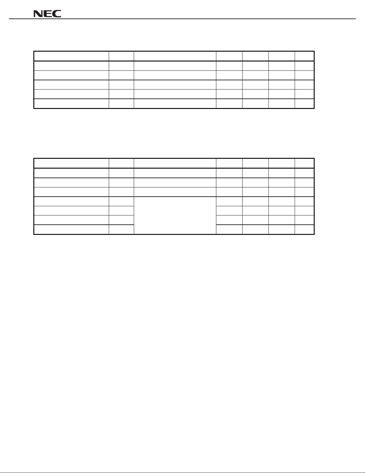
NES1823P-100
55
50
45
40
35
(dBm)
out
30
Output Power P
OUTPUT POWER, DRAIN CURRENT AND EFFICIENCY
POWER MATCHING
vs. INPUT POWER
P
out
η
D
I
D
80
70
60
50
(%)
40
D
η
30
Drain Efficiency
(A)
D
Drain Current I
25
20
15
10
20 25 30 35 40 45
Input Power Pin (dBm)
V
DS
f
g
R
20
10
0
–10
= 10 V
= 2.2 GHz
= 12.5 Ω
Dset
= 2 A
I
Dset
= 4 A
I
Dset
= 6 A
I
Preliminary Data Sheet4
Page 5
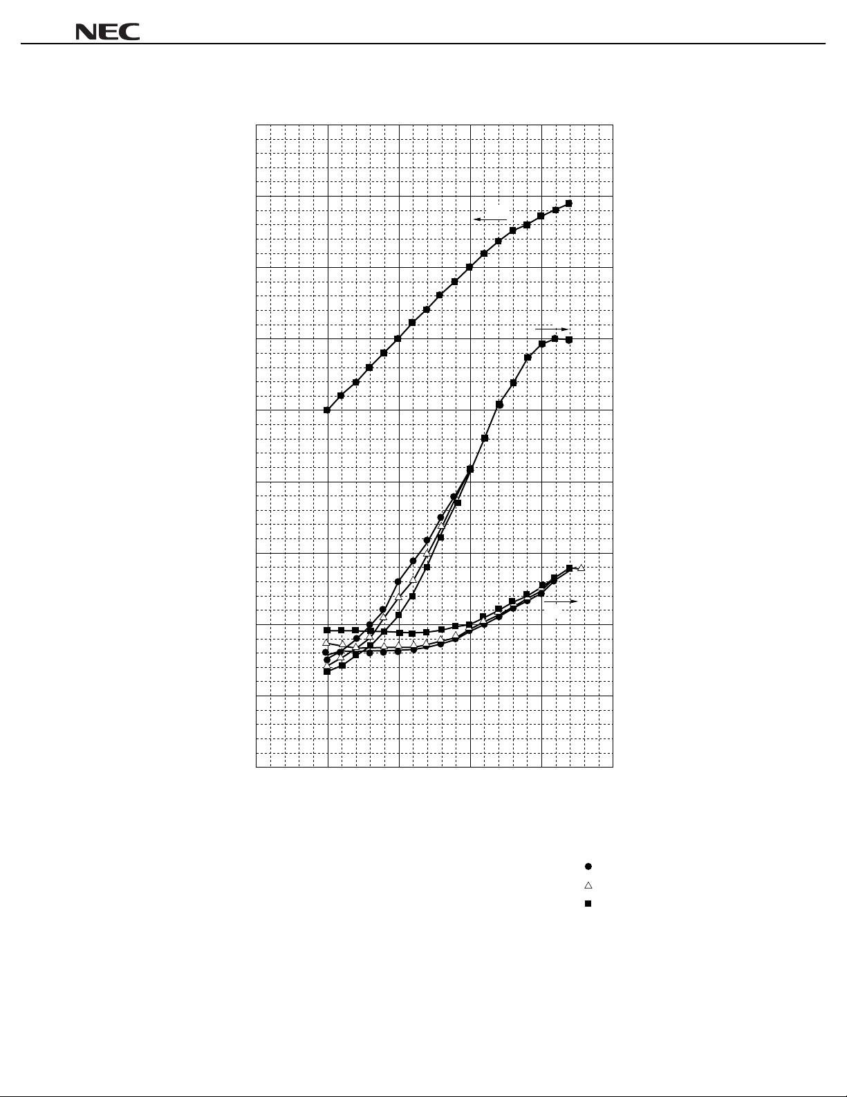
NES1823P-100
55
50
45
40
35
(dBm)
out
30
Output Power P
OUTPUT POWER, DRAIN CURRENT AND EFFICIENCY
DISTORTION MATCHING
vs. INPUT POWER
P
out
η
D
80
70
60
50
(%)
40
D
η
30
Drain Efficiency
(A)
D
Drain Current I
25
I
D
20
15
10
20 25 30 35 40 45
Input Power Pin (dBm)
V
DS
= 10 V
f
= 2.12 GHz
g
R
= 12.5 Ω
Dset
I
Dset
I
Dset
I
20
10
0
–10
= 6 A
= 8 A
= 10 A
Preliminary Data Sheet 5
Page 6
NES1823P-100
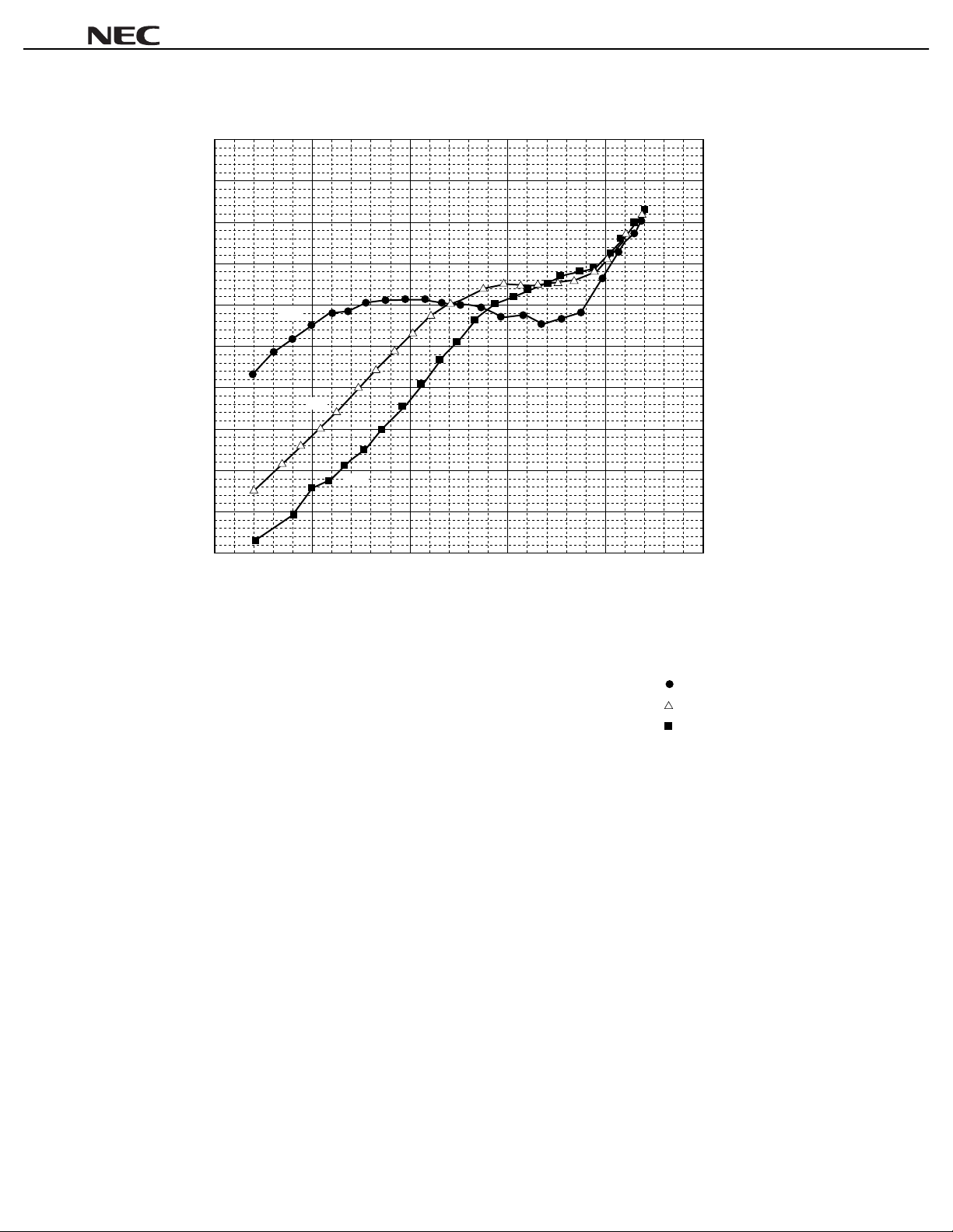
3rd INTERMODULATION DISTORTION vs.
2 TONES OUTPUT POWER
–10
–15
–20
(dBc)
3
–25
–30
2A
–35
–40
4A
3rd Intermodulation Distortion IM
–45
–50
–55
POWER MATCHING
6A
–60
25 30 35 40 45 50
2 tones Output Power P
out
(2 tones) (dBm)
V
f
∆
f
R
DS
g
= 10 V
= 1 MHz
= 2.2 GHz
= 12.5 Ω
Dset
= 2 A
I
Dset
= 4 A
I
Dset
= 6 A
I
Preliminary Data Sheet6
Page 7

NES1823P-100
3rd INTER MODULATION DISTORTION vs.
DISTORTION MATCHING
2TONES OUTPUT POWER
–10
–15
–20
–25
–30
–35
–40
–45
3rd Intermodulation Distortion IM3 (dBc)
–50
–55
–60
25 30 35 40 45 50
2 tones Output Power Pout (2 tones) (dBm)
V
DS
= 10 V
f
= 1 MHz
∆
f
= 2.12 GHz
g
R
= 12.5 V
Dset = 6 A
I
Dset = 8 A
I
Dset = 10 A
I
Preliminary Data Sheet 7
Page 8

NES1823P-100
3rd INTER MODULATION DISTORTION vs.
DISTORTION MATCHING
2TONES OUTPUT POWER
–10
–15
–20
–25
–30
–35
–40
–45
3rd Intermodulation Distortion IM3 (dBc)
–50
–55
–60
25 30 35 40 45 50
2 tones Output Power Pout (2 tones) (dBm)
DS
= 10 V
V
f
= 20 MHz
∆
f
= 2.12 GHz
g
R
= 12.5 Ω
Dset = 6 A
I
Dset = 8 A
I
Dset = 10 A
I
Preliminary Data Sheet8
Page 9

NES1823P-100
S-Parameters
DS
V
= 10 V, I
START 1 GHz, STOP 3 GHz, STEP 40 MHz Marker 2.2 GHz
Dset
= 3 A each drain
S
11
S
12
1.0
0.5
0
–0.5
+135° +45°
120.5
–1.0
S
21
+90°
–2.0
R
2.0
max
. = 1
+90°
+135° +45°
∞
±180° 0°
–135°
0.5
–90°
S
1.0
22
–45°
max
. = 0.1
R
2.0
±180° 0°
–135°
–90°
–45°
max
. = 5
R
Preliminary Data Sheet 9
0
0.5
–0.5
1
–1.0
2
–2.0
R
max
. = 1
∞
Page 10

S-Parameters
VDS = 10 V, I
Dset
= 3 A each drain
NES1823P-100
FREQUENCY S
11
21
S
12
S
GHz MAG. ANG. MAG. ANG. MAG. ANG. MAG. ANG.
1.000
1.040
1.080
1.120
1.160
1.200
1.240
1.280
1.320
1.360
1.400
1.440
1.480
1.520
1.560
1.600
1.640
1.680
1.720
1.760
1.800
1.840
1.880
1.920
1.960
2.000
2.040
2.080
2.120
2.160
2.200
2.240
2.280
2.320
2.360
2.400
2.440
2.480
2.520
2.560
2.600
2.640
2.680
2.720
2.760
2.800
2.840
2.880
2.920
2.960
3.000
0.959
0.959
0.956
0.956
0.956
0.950
0.946
0.941
0.941
0.935
0.927
0.920
0.912
0.903
0.890
0.876
0.858
0.839
0.815
0.789
0.756
0.719
0.674
0.616
0.548
0.474
0.405
0.371
0.403
0.477
0.553
0.622
0.664
0.693
0.712
0.719
0.723
0.721
0.713
0.701
0.684
0.661
0.632
0.594
0.542
0.483
0.499
0.530
0.555
0.587
0.625
173.5
172.7
171.7
170.8
170.8
168.7
167.5
166.2
164.8
163.3
161.7
159.9
158.1
156.0
153.9
151.5
149.1
146.6
143.8
141.2
138.1
135.1
132.1
129.1
127.3
127.6
132.9
144.4
156.0
160.5
159.4
155.8
150.3
144.6
138.7
132.7
127.3
120.8
114.1
106.5
98.3
88.7
78.0
65.6
51.8
40.7
29.6
10.9
–9.1
–28.3
–46.2
0.857
0.537
0.478
0.429
0.419
0.408
0.424
0.416
0.475
0.540
0.577
0.728
0.780
0.956
1.001
1.183
1.262
1.364
1.542
1.585
1.823
1.968
2.157
2.379
2.757
2.806
3.193
3.181
3.141
3.069
2.740
2.545
2.246
2.008
1.732
1.576
1.333
1.181
1.131
0.887
0.965
0.751
0.851
0.727
0.735
0.650
0.714
0.636
0.689
0.654
0.625
65.1
58.8
57.7
58.5
59.5
62.7
60.9
66.8
68.3
68.3
67.2
66.4
59.2
55.2
46.2
41.6
30.6
24.7
16.7
6.3
3.4
–11.4
–16.4
–28.8
–40.5
–54.6
–70.0
–85.4
–103.6
–118.7
–133.2
–150.0
–157.0
–175.7
–178.2
165.7
161.8
156.5
149.7
145.0
142.0
135.7
134.8
125.7
119.7
119.2
109.0
106.7
94.9
88.7
72.9
0.006
0.006
0.006
0.007
0.007
0.008
0.008
0.009
0.009
0.010
0.012
0.012
0.014
0.015
0.017
0.018
0.021
0.022
0.025
0.028
0.030
0.036
0.038
0.044
0.045
0.054
0.055
0.059
0.058
0.054
0.051
0.048
0.042
0.036
0.038
0.031
0.033
0.029
0.028
0.028
0.028
0.026
0.027
0.026
0.023
0.022
0.020
0.023
0.023
0.022
0.024
62.5
57.4
53.7
51.0
48.3
47.1
43.5
43.8
37.8
34.8
32.1
28.6
20.2
18.9
9.6
7.7
–1.8
–8.4
–18.3
–25.1
–36.7
–45.7
–58.5
–74.2
–85.5
–103.2
–120.7
–140.4
–159.5
–179.6
168.1
147.2
135.8
123.9
114.5
100.7
94.9
80.3
74.3
65.5
46.9
44.9
27.6
18.4
3.4
–5.7
–7.0
–15.0
–24.8
–36.4
–47.5
0.943
0.924
0.922
0.914
0.904
0.898
0.880
0.866
0.851
0.832
0.814
0.794
0.776
0.758
0.739
0.720
0.701
0.683
0.663
0.644
0.625
0.606
0.583
0.563
0.535
0.499
0.461
0.436
0.443
0.483
0.543
0.605
0.660
0.708
0.749
0.783
0.804
0.823
0.848
0.860
0.875
0.882
0.894
0.900
0.907
0.915
0.917
0.923
0.928
0.931
0.932
22
S
171.2
166.7
165.7
164.2
162.7
161.5
159.8
158.2
156.4
154.7
152.8
150.9
148.9
146.8
144.5
142.0
139.5
136.7
133.6
130.0
125.8
120.5
113.6
104.6
91.7
74.1
50.3
19.8
–14.0
–44.9
–69.8
–89.0
–103.5
–115.0
–124.2
–131.9
–136.9
–142.7
–147.4
–151.8
–155.2
–158.4
–161.5
–163.8
–166.2
–168.7
–170.4
–172.2
–174.0
–175.7
–177.1
Preliminary Data Sheet10
Page 11

NES1823P-100
CIRCUIT DESIGN
The matching circuit of package inside consists of bond-wire, chip-capacitor and microstrip line on the alumina
substrate. The package-lead impedance is designed as 25 Ω connecting to the external matching circuit, in the
external circuit design, the microstrip line impedance is 25 Ω, conjugate with package impedance, then the
impedance is connected to balun, it is 1:2 balun structure, finally connected to 50 Ω. Balun technology has some
advantage over single-ended device, minimize matching-loss with decrease of impedance change ratio and cancel
the even mode harmonic frequency for IM
BALUN DESIGN
The balun design is the key for these high power push-pull structure device. NEC designed low insertion loss
microstrip balun for this product. What is the reason of our choice? One is the repeatability of assembly, and the
other is its performance. Microstrip balun performance tolerance is small because of its simple structure. So the
balun performance is stable and repeatable between NEC and customers. And its insertion loss is 0.2 dB less than
coaxial balun 0.3 dB, also Its band width is better than coaxial balun. The microstrip balun is consists of microstrip
pattern and cavity, therefore its insertion loss and band width due to its parameter design. Those parameters are
optimized with simuration. : (substrate duroid ε r = 2.2 t = 0.8 mm)
Then the phase difference between two ports is 180° ±4, insertion loss is 0.2 dB from 1 to 3 GHz.
3
performance. The balun circuit is employed for this product.
DC STABILITY (AVOID OSCILLATION)
The function of DC-cut capacitor arranged between transformer and microstrip balun is avoid DC oscillation.
When the gate is pinch-off, a few pinch-off voltage (VP) difference of each port occur the loop current, then start DC
oscillation in the area of pinch-off. Because of this reasons, the DC-cut capacitor is need to this microstrip balun
assemble. Additionally, the ground of transformer substate is effective to DC oscillation, so that five screws are
arranged at the middle of substrate.
Preliminary Data Sheet 11
Page 12

RF TEST FIXTURE
Input MS Balun Output MS Balundevice
NES1823P-100
180˚
50 Ω
IN OUT
0˚
Input MS Balun Output MS Balun
DC CUT
25 Ω
25 Ω 25 Ω
1 000 pF
µ
4.7 F
transformer transformer
Rg=5 Ω
25 Ω
0˚
180˚
µ
4.7 F
DC CUT 20 pF × 2
50 Ω
OUT
IN
cavity (depth = 1.2 mm)
Series R = 510 Ω
39 pF
1 000 pF
4.7 F
µ
g
= 10 Ω
R
device
chip C 2.2 F
VGS
µ
VDS
1 000 pF
4.7 F
cavity (depth = 1.2 mm)
µ
Preliminary Data Sheet12
Page 13

FIGURES OF SUBSTRATE (UNIT: mm)
BALUN (FACE)
10.75
8.25
2.78
0
35.25
33.25
38.75
39.75
37.75
41.75
59.25
+0
72.22
NES1823P-100
–0.1
75
0
18
20.5
C2.5
φ
6 – 3
BALUN (BACK)
0
3.08
5 adjusting patterns at a 0.5 mm pitch
17
19
20
2-C5.5
2-C1.5
0
22.75
28.25
33.75
41.25
49.5
46.75
5.3
0.5
52.25
0.5
0.5
61.01
20.5
23
28.5
41
43.13
46.92
+0
50
–0.1
22.5
46.5
65.517
10
7.5
13.5
21.5
34.5
49.5
19.520.5
9
6.5
3
1.5
61
Preliminary Data Sheet 13
Page 14

TRANSFORMER
75
70
65
30
+0
–0.1
NES1823P-100
92 –
18.8
2
1
7.8
5 – 3.5
φ
4 – 3
φ
3.5555
3
1
+0
–0.1
30
15
1
10
2.5 5
4 1 4.5 2 4 4
15.5
1.8 6.5
1
16 – 1
φ
through hole
2
1
10
7
3
2
35
61
61.5
t = 0.8 mm
ε
r
= 2.2
Preliminary Data Sheet14
Page 15

PACKAGE DIMENSIONS (UNIT: mm)
NES1823P-100
35.2 ± 0.3
9.7 ± 0.3
2.4 ± 0.3
R1.2 ± 0.3
2.4 ± 0.2
G1, G2: Gate
D2: Drain
D1,
S
: Source
45˚
S
G1 G2
D1 D2
4.0 ± 0.3
31.6 ± 0.3
S
8.0
17.4 ± 0.3
4.75 MAX.
1.8 ± 0.2
Preliminary Data Sheet 15
Page 16

NES1823P-100
RECOMMENDED MOUNTING CONDITION FOR CORRECT USE
(1) Fix to a heatsink or mount surface completely with screw at the four holes of the flange.
(2) Recommended torque strength of the screw is 3 kgF typical using M2.3 type screw.
(3) Recommended flatness of the mount surface is less than ±10 µm. (roughness of surface is )
RECOMMENDED SOLDERING CONDITIONS
This product should be soldered under the following recommended conditions. For soldering methods and
conditions other than those recommended below, contact your NEC sales representative.
Soldering Method Soldering Conditions Recommended Condition Symbol
Partial Heating Pin temperature: 260°C
Time: 5 seconds or less (per pi n row)
For details of recommended soldering conditions, please contact your local NEC sales office.
–
Preliminary Data Sheet16
Page 17

[MEMO]
NES1823P-100
Preliminary Data Sheet 17
Page 18

[MEMO]
NES1823P-100
Preliminary Data Sheet18
Page 19

[MEMO]
NES1823P-100
Preliminary Data Sheet 19
Page 20

NES1823P-100
Caution
The Great Care must be taken in dealing with the devices in this guide.
The reason is that the material of the devices is GaAs (Gallium Arsenide), which is
designated as harmful substance according to the law concerned.
Keep the law concerned and so on, especially in case of removal.
No part of this document may be copied or reproduced in any form or by any means without the prior written
consent of NEC Corporation. NEC Corporation assumes no responsibility for any errors which may appear in this
document.
NEC Corporation does not assume any liability for infringement of patents, copyrights or other intellectual
property rights of third parties by or arising from use of a device described herein or any other liability arising
from use of such device. No license, either express, implied or otherwise, is granted under any patents,
copyrights or other intellectual property rights of NEC Corporation or others.
While NEC Corporation has been making continuous effort to enhance the reliability of its semiconductor devices,
the possibility of defects cannot be eliminated entirely. To minimize risks of damage or injury to persons or
property arising from a defect in an NEC semiconductor device, customers must incorporate sufficient safety
measures in its design, such as redundancy, fire-containment, and anti-failure features.
NEC devices are classified into the following three quality grades:
"Standard", "Special", and "Specific". The Specific quality grade applies only to devices developed based on
a customer designated "quality assurance program" for a specific application. The recommended applications
of a device depend on its quality grade, as indicated below. Customers must check the quality grade of each
device before using it in a particular application.
Standard: Computers, office equipment, communications equipment, test and measurement equipment,
audio and visual equipment, home electronic appliances, machine tools, personal electronic
equipment and industrial robots
Special: Transportation equipment (automobiles, trains, ships, etc.), traffic control systems, anti-disaster
systems, anti-crime systems, safety equipment and medical equipment (not specifically designed
for life support)
Specific: Aircrafts, aerospace equipment, submersible repeaters, nuclear reactor control systems, life
support systems or medical equipment for life support, etc.
The quality grade of NEC devices is "Standard" unless otherwise specified in NEC's Data Sheets or Data Books.
If customers intend to use NEC devices for applications other than those specified for Standard quality grade,
they should contact an NEC sales representative in advance.
Anti-radioactive design is not implemented in this product.
M4 96. 5
 Loading...