

Page 1
DATA SHEET
N-CHANNEL GaAs HJ-FET
NE6510179A
1 W L-BAND POWER GaAs HJ-FET
DESCRIPTION
The NE6510179A is a 1 W GaAs HJ-FET designed for middle power transmitter applications for mobile
communication and wireless PC LAN systems. It is capable of delivering 1 W of output power (CW) with high linear
gain, high efficiency and excellent distortion.
Reliability and performance uniformity are assured by NEC’s stringent quality and control procedures.
FEATURES
• GaAs HJ-FET structure
• High output power : P
out
= +31.5 dBm TYP. @VDS = 3.5 V, I
out
P
= +32.5 dBm TYP. @VDS = 3.5 V, I
out
P
= +35.0 dBm TYP. @VDS = 5.0 V, I
• High linear gain : GL = 15 dB TYP. @VDS = 3.5 V, I
GL = 10 dB TYP. @VDS = 3.5 V, I
GL = 10 dB TYP. @VDS = 5.0 V, I
• High power added efficiency : 70% TYP. @VDS = 3.5 V, I
58% TYP. @VDS = 3.5 V, I
56% TYP. @VDS = 5.0 V, I
Dset
= 200 mA, f = 900 MHz, Pin = +20 dBm
Dset
= 200 mA, f = 1 900 MHz, Pin = +25 dBm
Dset
= 200 mA, f = 1 900 MHz, Pin = +25 dBm
Dset
= 200 mA, f = 900 MHz, Pin = +20 dBm
Dset
= 200 mA, f = 1 900 MHz, Pin = +25 dBm
Dset
= 200 mA, f = 1 900 MHz, Pin = +25 dBm
Dset
= 200 mA, f = 900 MHz, Pin = 0 dBm
Dset
= 200 mA, f = 1 900 MHz, Pin = 0 dBm
Dset
= 200 mA, f = 1 900 MHz, Pin = 0 dBm
ORDERING INFORMATION
Part Number Package Supplying Form
NE6510179A-T1 79A
Remark
Caution Please handle this device at static-free workstation, because this is an electrostatic sensitive
Document No. P13496EJ4V0DS00 (4th edition)
Date Published August 2000 N CP(K)
Printed in Japan
To order evaluation samples, consult your NEC sales representative
(Part number for sample order: NE6510179A).
device.
The information in this document is subject to change without notice. Before using this document, please
confirm that this is the latest version.
Not all devices/types available in every country. Please check with local NEC representative for
availability and additional information.
•
12 mm wide embossed taping
•
Qty 1 kpcs/reel
The mark shows major revised points.
©
1998, 2000
Page 2
ABSOLUTE MAXIMUM RATINGS (TA = +25°C)
Operation in excess of any one of these parameters may result in permanent damage.
Parameter Symbol Ratings Unit
Drain to Source Voltage V
Gate to Source Voltage V
Drain Current I
Gate Forward Current I
Gate Reverse Current I
Total Power Dissipat i on P
Channel Temperature T
Storage Temperature T
DS
GSO
D
GF
GR
tot
ch
stg
8V
–4 V
2.8 A
25 mA
25 mA
15 W
150 °C
–65 to +150 °C
RECOMMENDED OPERATING CONDITIONS
Parameter Symbol Test Condition MIN. TYP. MAX. Unit
NE6510179A
Drain to Source Voltage V
DS
Gain Compression Gcomp
Channel Temperature T
Recommended maximum Gain Compression is 3.0 dB at V
Note
ch
DS
> 4.2 V
ELECTRICAL CHARACTERISTICS
(TA = +25°C, unless otherwise specified, using NEC standard test fixture.)
Parameter Symbol Test Conditions MIN. TYP. MAX. Unit
BV
η
DSS
add
G
VDS = 2.5 V, VGS = 0 V
p
VDS = 2.5 V, ID = 14 mA –2.0
gd
Igd = 14 mA 12
th
Channel to Case
out
D
f = 1.9 GHz, VDS = 3.5 V,
in
= +25 dBm, Rg = 100 Ω,
P
Dset
= 200 mA (RF OFF)
I
Note 2
L
Saturated Drain Current I
Pinch-off Voltage V
Gate to Drain Break Down
Voltage
Thermal Resistance R
Output Power P
Drain Current I
Power Added Efficiency
Linear Gain
Note 1
−
3.5 5.5 V
−−
−−
−
2.4
−
−−
−
58°C/W
31.5 32.5
−
0.72
50 58
−
10.0
Note
5.0
+110 °C
−
–0.4 V
−
dBm
−
−
−
dB
A
V
A
%
dB
Notes 1.
2
in
= 0 dBm
P
DC performance is 100% testing. RF performance is testing several samples per wafer.
2.
Wafer rejection criteria for standard devices is 1 reject for several samples.
Data Sheet P13496EJ4V0DS00
Page 3
TYPICAL RF PERFORMANCE FOR REFERENCE
(TA = +25°C, unless otherwise specified, using NEC standard test fixture.)
Parameter Symbol Test Conditions MIN. TYP. MAX. Unit
NE6510179A
Output Power P
Drain Current I
Power Added Efficiency
Linear Gain
Note
Note
in
= 0 dBm
P
out
D
η
add
G
f = 900 MHz, VDS = 3.5 V,
in
= +20 dBm, Rg = 100 Ω,
P
Dset
= 200 mA (RF OFF)
I
L
TYPICAL RF PERFORMANCE FOR REFERENCE
(TA = +25°C, unless otherwise specified, using NEC standard test fixture.)
Parameter Symbol Test Conditions MIN. TYP. MAX. Unit
Output Power P
Drain Current I
Power Added Efficiency
Linear Gain
Note
Note
in
= 0 dBm
P
out
D
η
add
G
f = 1.9 GHz, VDS = 5.0 V,
in
= +25 dBm, Rg = 100 Ω,
P
Dset
= 200 mA (RF OFF)
I
L
TYPICAL CHARACTERISTICS (TA = +25°°°°C)
−
−
−
−
−
−
−
−
31.5
0.53
70
15.0
35.0
1.2
56
10.0
−
−
−
−
−
−
−
−
dBm
A
%
dB
dBm
A
%
dB
(dBm)
out
Output Power P
Remark
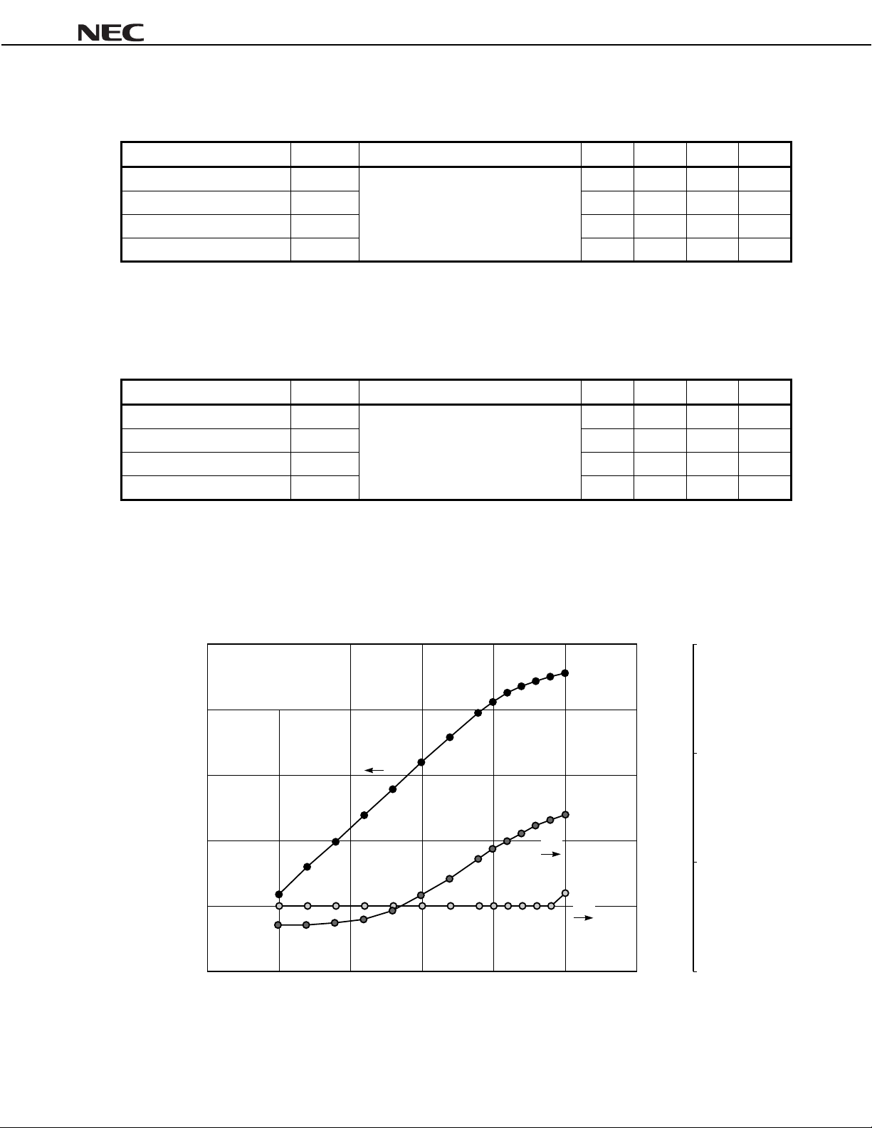
OUTPUT POWER, DRAIN CURRENT AND GATE CURRENT vs. INPUT POWER
35
VDS = 3.5 V
Dset
= 200 mA (RF OFF)
I
g
= 100 Ω
R
f = 1.9 GHz
30
P
out
25
20
15
10
Input Power Pin (dBm)
I
D
I
G
The graph indicates nominal characteristics.
8
6
4
2
0
–2
302520151050
1 500
1 000
(mA)
G
Gate Current I
500
0
(mA)
D
Drain Current I
Data Sheet P13496EJ4V0DS00
3
Page 4

S-PARAMETERS
NE6510179A
Test Conditions: VDS = 3.5 V, I
Frequency S
= 200 mA (RF OFF)
Dset
11
21
S
12
S
S
MHz MAG. ANG. (deg.) MAG. ANG. (deg.) MAG. ANG. (deg.) MAG. ANG. (deg.)
550 0.940 179.9 2.859 92.3 0.020 21.9 0.803 177.2
600 0.938 178.6 2.699 92.6 0.020 24.3 0.808 177.2
650 0.943 177.5 2.440 91.9 0.020 25.3 0.806 176.5
700 0.940 176.9 2.316 91.5 0.021 26.7 0.807 176.3
750 0.939 175.8 2.098 91.2 0.020 28.0 0.802 175.3
800 0.948 175.1 2.008 90.3 0.021 29.6 0.796 175.5
850 0.949 174.9 1.826 92.0 0.020 31.2 0.802 173.7
900 0.938 174.1 1.772 90.5 0.022 32.0 0.804 174.5
950 0.940 173.2 1.691 92.5 0.020 36.4 0.808 173.7
1000 0.940 172.4 1.579 90.2 0.022 34.6 0.807 173.5
1050 0.940 171.9 1.545 92.7 0.021 39.3 0.806 172.8
1100 0.938 171.7 1.447 91.4 0.022 37.3 0.805 172.3
1150 0.940 171.1 1.432 91.0 0.022 40.5 0.807 171.9
1200 0.936 170.4 1.342 90.6 0.023 40.4 0.803 171.4
1250 0.935 170.1 1.325 91.3 0.022 42.5 0.803 171.3
1300 0.935 169.4 1.224 89.2 0.023 42.3 0.800 170.8
1350 0.933 169.9 1.232 90.2 0.023 47.0 0.806 171.4
1400 0.934 168.0 1.140 90.0 0.023 45.5 0.795 169.9
1450 0.937 167.5 1.105 88.5 0.024 46.1 0.804 169.5
1500 0.938 167.0 1.075 90.0 0.023 49.5 0.801 168.8
1550 0.938 166.4 1.045 90.3 0.024 49.6 0.803 168.7
1600 0.934 167.1 1.019 91.1 0.024 52.3 0.803 169.5
1650 0.936 165.1 0.997 89.7 0.025 53.3 0.803 167.6
1700 0.933 164.6 0.982 91.0 0.025 54.8 0.800 166.7
1750 0.934 163.7 0.936 89.6 0.026 54.6 0.803 166.6
1800 0.934 162.9 0.961 87.4 0.026 57.7 0.799 165.3
1850 0.934 162.1 0.905 90.9 0.026 55.6 0.804 165.4
1900 0.935 161.7 0.875 85.8 0.028 58.5 0.798 164.1
1950 0.931 160.7 0.855 89.3 0.026 58.2 0.800 164.1
2000 0.929 160.4 0.807 87.2 0.028 59.5 0.797 163.2
2050 0.929 158.8 0.796 89.3 0.027 58.0 0.802 162.6
2100 0.933 158.1 0.772 85.5 0.028 63.2 0.797 161.1
2150 0.928 156.6 0.769 92.6 0.027 60.2 0.792 160.5
2200 0.934 156.5 0.729 87.0 0.028 65.2 0.793 159.9
2250 0.930 155.5 0.716 92.2 0.027 65.6 0.795 159.9
22
4
Data Sheet P13496EJ4V0DS00
Page 5

APPLICATION CIRCUIT EXAMPLE
f = 1.9 GHz (Unit: mm)
NE6510179A
GS
V
R
g
V
DS
Tantalum Condenser
47 F
µ
/4 OPEN STUB
λ
5
2
C1
3
4
3
INPUT
12
f = 1.9 GHz
DS
= 3.5 V
V
I
Dset
= 200 mA (RF OFF)
APPLICATION CIRCUIT EXAMPLE
f = 900 MHz (Unit: mm)
1 000 p
λ
/4 LINE
5
16 16
22
42
C1 = 30 pF
C2 = 30 pF
GS VDS
V
4
6
g
R
2
3
= 100 Ω
39.5
Tantalum Condenser
100 F
µ
/4 OPEN STUB
λ
50 Ω LINE
5
GND
Substrate: Teflon glass ( r = 2.6)
t = 0.8 mm
C2
3
3
OUTPUT
ε
Tantalum Condenser
2
C1
INPUT
f = 900 MHz
V
DS = 3.5 V
I
Dset = 200 mA (RF OFF)
47 F
µ
/4 OPEN STUB
λ
3
6
C4
Rg
12
1.5
2
4
182
3
C5
C1 = 30 pF C5 = 8 pF
C2 = 30 pF
C3 = 30 pF
C6 = 8 pF
C7 = 4 pF
C4 = 3 pF
1 000 p
λ
/4 LINE
211
5
R1
C3
6
1
C6
R1 = 30 Ω
g = 100 Ω
R
Tantalum Condenser
100 F
µ
λ
/4 OPEN STUB
5
4
2
1.5
203
2.5
2
6
50 Ω LINE
31
3
C2
2.5
OUTPUT
C7
GND
Substrate: Teflon glass ( r = 2.6)
ε
t = 0.8 mm
Data Sheet P13496EJ4V0DS00
5
Page 6

79A PACKAGE DIMENSIONS (Unit: mm)
4.2 MAX.
Source
NE6510179A
BOTTOM VIEW
1.5±0.2
Source
Gate
0.6±0.15
5.7 MAX.
0.9±0.2
T I
0.4±0.15
5.7 MAX.
Drain
4.4 MAX.
0.8±0.15
8X
0.2±0.1
Gate
1.0 MAX.
79A PACKAGE RECOMMENDED P.C.B. LAYOUT (Unit: mm)
4.0
1.7
Drain
1.2 MAX.
0.8 MAX.
3.6±0.2
Stop up the hole with a rosin
or something to avoid solder
flow.
Drain Gate
5.9
6
1.2
Source
0.5
0.5 0.5
6.1
Data Sheet P13496EJ4V0DS00
through hole 0.2 × 33
φ
1.0
Page 7

NE6510179A
RECOMMENDED SOLDERING CONDITIONS
This product should be soldered and mounted under the following recommended conditions. For soldering
methods and conditions other than those recommended below, contact your NEC sales representative.
Soldering Method Soldering Conditions Recommended Condition Symbol
Infrared Reflow Package peak temperature: 235°C or below,
Time: 30 seconds or less (at 210°C or higher),
Count: 2 times or less,
Exposure limit: None
Partial Heating Pin temperature: 260°C or below,
Time: 5 seconds or less (per pi n row),
Exposure limit: None
After opening the dry pack, store it at 25°C or less and 65% RH or less for the allowable storage period.
Note
Note
Note
Caution Do not use different soldering methods together (except for partial heating).
IR35-00-2
–
Data Sheet P13496EJ4V0DS00
7
Page 8

NE6510179A
CAUTION
The great care must be taken in dealing with the devices in this guide.
The reason is that the material of the devices is GaAs (Gallium Arsenide), which is
designated as harmful substance according to the law concerned.
Keep the law concerned and so on, especially in case of removal.
•
The information in this document is current as of August, 2000. The information is subject to
change without notice. For actual design-in, refer to the latest publications of NEC's data sheets or
data books, etc., for the most up-to-date specifications of NEC semiconductor products. Not all
products and/or types are available in every country. Please check with an NEC sales representative
for availability and additional information.
•
No part of this document may be copied or reproduced in any form or by any means without prior
written consent of NEC. NEC assumes no responsibility for any errors that may appear in this document.
•
NEC does not assume any liability for infringement of patents, copyrights or other intellectual property rights of
third parties by or arising from the use of NEC semiconductor products listed in this document or any other
liability arising from the use of such products. No license, express, implied or otherwise, is granted under any
patents, copyrights or other intellectual property rights of NEC or others.
•
Descriptions of circuits, software and other related information in this document are provided for illustrative
purposes in semiconductor product operation and application examples. The incorporation of these
circuits, software and information in the design of customer's equipment shall be done under the full
responsibility of customer. NEC assumes no responsibility for any losses incurred by customers or third
parties arising from the use of these circuits, software and information.
•
While NEC endeavours to enhance the quality, reliability and safety of NEC semiconductor products, customers
agree and acknowledge that the possibility of defects thereof cannot be eliminated entirely. To minimize
risks of damage to property or injury (including death) to persons arising from defects in NEC
semiconductor products, customers must incorporate sufficient safety measures in their design, such as
redundancy, fire-containment, and anti-failure features.
•
NEC semiconductor products are classified into the following three quality grades:
"Standard", "Special" and "Specific". The "Specific" quality grade applies only to semiconductor products
developed based on a customer-designated "quality assurance program" for a specific application. The
recommended applications of a semiconductor product depend on its quality grade, as indicated below.
Customers must check the quality grade of each semiconductor product before using it in a particular
application.
"Standard": Computers, office equipment, communications equipment, test and measurement equipment, audio
and visual equipment, home electronic appliances, machine tools, personal electronic equipment
and industrial robots
"Special": Transportation equipment (automobiles, trains, ships, etc.), traffic control systems, anti-disaster
systems, anti-crime systems, safety equipment and medical equipment (not specifically designed
for life support)
"Specific": Aircraft, aerospace equipment, submersible repeaters, nuclear reactor control systems, life
support systems and medical equipment for life support, etc.
The quality grade of NEC semiconductor products is "Standard" unless otherwise expressly specified in NEC's
data sheets or data books, etc. If customers wish to use NEC semiconductor products in applications not
intended by NEC, they must contact an NEC sales representative in advance to determine NEC's willingness
to support a given application.
(Note)
(1) "NEC" as used in this statement means NEC Corporation and also includes its majority-owned subsidiaries.
(2) "NEC semiconductor products" means any semiconductor product developed or manufactured by or for
NEC (as defined above).
M8E 00. 4
 Loading...