

Page 1

Philips Semiconductors
SA614A
Low power FM IF system
Product specification
Replaces data of December 15, 1994
1997 Nov 07
RF COMMUNICATIONS PRODUCTS
IC17 Data Handbook
Page 2
Philips Semiconductors Product specification
SA614ALow power FM IF system
2
1997 Nov 07 853-0594 18663
DESCRIPTION
The SA614A is an improved monolithic low-power FM IF system
incorporating two limiting intermediate frequency amplifiers,
quadrature detector, muting, logarithmic received signal strength
indicator, and voltage regulator. The SA614A features higher IF
bandwidth (25MHz) and temperature compensated RSSI and
limiters permitting higher performance application compared with the
SA604. The SA614A is available in a 16-lead dual-in-line plastic
and 16-lead SO (surface-mounted miniature) package.
FEA TURES
•Low power consumption: 3.3mA typical
•Temperature compensated logarithmic Received Signal Strength
Indicator (RSSI) with a dynamic range in excess of 90dB
•Two audio outputs - muted and unmuted
•Low external component count; suitable for crystal/ceramic filters
•Excellent sensitivity: 1.5µV across input pins (0.22µV into 50Ω
matching network) for 12dB SINAD (Signal to Noise and Distortion
ratio) at 455kHz
•SA614A meets cellular radio specifications
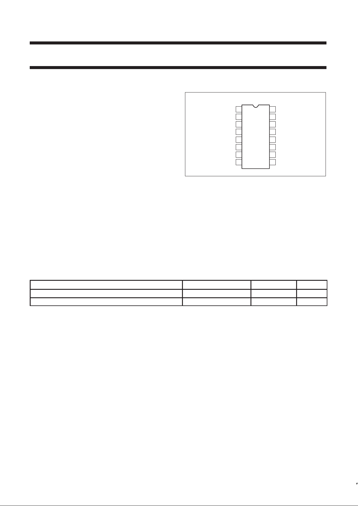
PIN CONFIGURATION
D and N Packages
IF AMP DECOUPLING
1
2
3
4
5
6
7
8
9
10
11
12
13
14
16
15
GND
MUTE INPUT
RSSI OUTPUT
MUTE AUDIO OUTPUT
UNMUTE AUDIO OUTPUT
QUADRATURE INPUT
IF AMP INPUT
IF AMP DECOUPLING
IF AMP OUTPUT
GND
LIMITER INPUT
LIMITER DECOUPLING
LIMITER DECOUPLING
LIMITER
V
CC
SR00323
Figure 1. Pin Configuration
APPLICATIONS
•Cellular radio FM IF
•High performance communications receivers
•Intermediate frequency amplification and detection up to 25MHz
•RF level meter
•Spectrum analyzer
•Instrumentation
•FSK and ASK data receivers
ORDERING INFORMATION
DESCRIPTION TEMPERATURE RANGE ORDER CODE DWG #
16-Pin Plastic Dual In-Line Package (DIP) -40 to +85°C SA614AN SOT38-4
16-Pin Plastic Small Outline (SO) package (Surface-mount) -40 to +85°C SA614AD SOT109-1
Page 3

Philips Semiconductors Product specification
SA614ALow power FM IF system
1997 Nov 07
3
BLOCK DIAGRAM
16 15 14 13 12 11 10 9
87654321
SIGNAL
VOLTAGE
IF
AMP
LIMITER
REGULATOR
STRENGTH
GND
V
CC
GND
MUTE
QUAD
DET
LIMITER
SR00324
Figure 2. Block Diagram
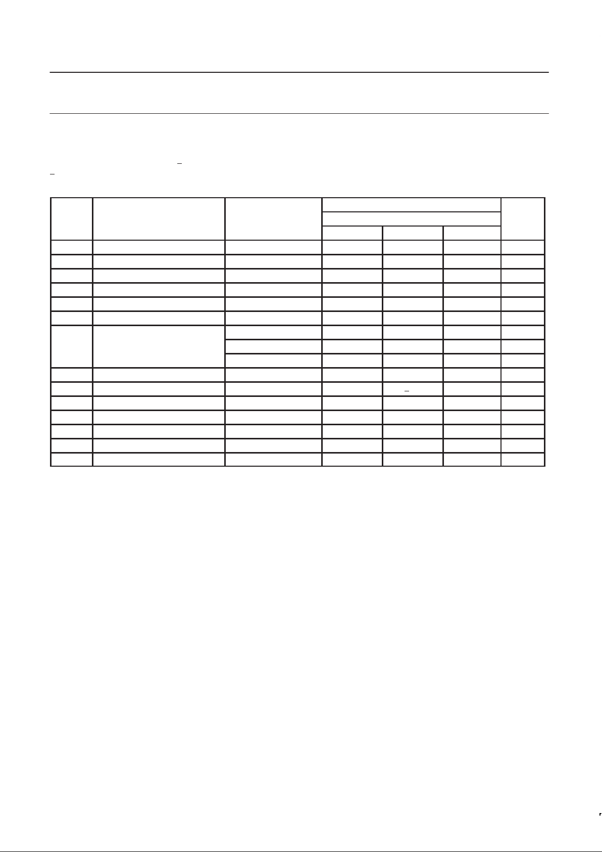
ABSOLUTE MAXIMUM RATINGS
SYMBOL PARAMETER RATING UNITS
V
CC
Single supply voltage 9 V
T
STG
Storage temperature range -65 to +150
°C
T
A
Operating ambient temperature range SA614A -40 to +85
°C
θ
JA
Thermal impedance D package
N package
90
75
°C/W
°C/W
DC ELECTRICAL CHARACTERISTICS
VCC = +6V, TA = 25°C; unless otherwise stated.
LIMITS
SYMBOL PARAMETER TEST CONDITIONS SA614A UNITS
MIN TYP MAX
V
CC
Power supply voltage range 4.5 8.0 V
I
CC
DC current drain 2.5 3.3 4.0 mA
Mute switch input threshold (ON)
(OFF)
1.7
1.0
V
V
Page 4
Philips Semiconductors Product specification
SA614ALow power FM IF system
1997 Nov 07
4
AC ELECTRICAL CHARACTERISTICS
Typical reading at TA = 25°C; VCC = +6V , unless otherwise stated. IF frequency = 455kHz; IF level = -47dBm; FM modulation = 1kHz with
+
8kHz peak deviation. Audio output with C-message weighted filter and de-emphasis capacitor. Test circuit Figure 3. The parameters listed
below are tested using automatic test equipment to assure consistent electrical characterristics. The limits do not represent the ultimate
performance limits of the device. Use of an optimized RF layout will improve many of the listed parameters.
LIMITS
SYMBOL PARAMETER TEST CONDITIONS SA614A UNITS
MIN TYP MAX
Input limiting -3dB Test at Pin 16 -92 dBm/50Ω
AM rejection 80% AM 1kHz 25 33 dB
Recovered audio level 15nF de-emphasis 60 175 260 mV
RMS
Recovered audio level 150pF de-emphasis 530 mV
RMS
THD Total harmonic distortion -30 -42 dB
S/N Signal-to-noise ratio No modulation for noise 68 dB
RF level = -118dBm 0 160 800 mV
RSSI output
1
RF level = -68dBm 1.7 2.50 3.3 V
RF level = -18dBm 3.6 4.80 5.8 V
RSSI range R4 = 100k (Pin 5) 80 dB
RSSI accuracy R4 = 100k (Pin 5) +2.0 dB
IF input impedance 1.4 1.6 kΩ
IF output impedance 0.85 1.0 kΩ
Limiter input impedance 1.4 1.6 kΩ
Unmuted audio output resistance 58 kΩ
Muted audio output resistance 58 kΩ
NOTE:
1. SA614A data sheets refer to power at 50Ω input termination; about 21dB less power actually enters the internal 1.5k input.
SA614A (50) SA614A (1.5k)/SA615 (1.5k)
-97dBm -118dBm
-47dBm -68dBm
+3dBm -18dBm
The SA615 and SA614A are both derived from the same basic die. The SA615 performance plots are directly applicable to the SA614A.
Page 5
Philips Semiconductors Product specification
SA614ALow power FM IF system
1997 Nov 07
5
IF INPUT
GND
RSSI AUDIO DATA
GND
GND
OFF
ON
V
CC
SIGNETICS
NE614 TEST CKT
M
U
T
E
100nF + 80 – 20% 63V K10000–25V Ceramic
455kHz Ceramic Filter Murata SFG455A3
100nF +
10% 50V
100nF +
10% 50V
455kHz (Ce = 180pF) TOKO RMC 2A6597H
51Ω +
1% 1/4W Metal Film
150pF +
2% 100V N1500 Ceramic
6.8µF +
20% 25V Tantalum
1nF +
10% 100V K2000-Y5P Ceramic
15nF +
10% 50V
100nF +
10% 50V
C1
C2
C3
C4
C5
C6
C7
C8
C9
C10
C11
C12
F1
F2
R1
100nF +10% 50V
100nF +
10% 50V
100nF +10% 50V
10pF +
2% 100V NPO Ceramic
R2
R3
R4
1500Ω +
1% 1/4W Metal Film
1500Ω +
5% 1/8W Carbon Composition
100kΩ +
1% 1/4W Metal Film
16 15 14 13 12 11 10 9
87654321
NE614A TEST CIRCUIT
SA614A
INPUT
Q = 20 LOADED
MUTE
INPUT
RSSI
OUTPUT
AUDIO
OUTPUT
DATA
OUTPUT
C
5
C
3
C
6
S
1
C
10
C
8
F
2
C
12
C
9
F
1
C
7
C
11
R
1
R
2
R
3
C
4
C
1
C
2
R
4
IF INPUT
GND
RSSI AUDIO DATA
GND
GND
OFF
ON
V
CC
SIGNETICS
NE614 TEST CKT
M
U
T
E
SR00325
Figure 3. SA614A Test Circuit
Page 6

Philips Semiconductors Product specification
SA614ALow power FM IF system
1997 Nov 07
6
16 15 14 13 11 10 9
87654321
12
42k
GND
42k
700
7k
1.6k
40k
700
35k
1.6k
40k
2k
4.5k
2k 8k
FULL
WAVE
RECT.
VOLTAGE/
CURRENT
CONVERTER
VOLT
REG
VOLT
REG
MUTE QUAD
DET
BAND
GAP
VOLT
GND
80k
55k
55k
40k
40k
80k
80k
FULL
WAVE
RECT.
V
EE
V
CC
V
CC
V
CC
SR00326
Figure 4. Equivalent Circuit
Page 7

Philips Semiconductors Product specification
SA614ALow power FM IF system
1997 Nov 07
7
16 15 14 13 12 11 10 9
87654321
NE604A TEST CIRCUIT
SA604A
MUTE
AUDIO
RSSI
DATA
8765
4321
SA602
+6V
100nF
10nF
47pF
22pF
100nF
5.6pF
44.545
3rd OVERTURE
XTAL
SFG455A3
OUT
OUT
C–MSG
FILTER
455kHz
Q=20
SFG455A3
+6V
4V
10pF
3V
2V
1V
–0
–20
–40
–60
–80
10 100 1k 10k 100k
–120 –100 –80 –60 –40 –20
AUDIO OUT – ‘C’ MESSAGE WEIGHTED
614A IF INPUT (µV) (1500Ω)
(0dB REF = RECOVERED AUDIO FOR
+8kHz PEAK DEVIATION (dB)
–
AUDIO
RSSI (VOLTS)
THD + NOISE
AM (80% MOD)
NOISE
602 RF INPUT (dBm) (50Ω)
0.1µF
0.1µF
0.1µF
0.1µF
0.1µF
22pF
1nF
0.5
to
1.3µH
5.5µH
6.8µF
0.21
to
0.28µH
100k
0.1µF
SR00327
Figure 5. Typical Application Cellular Radio (45MHz to 455kHz)
CIRCUIT DESCRIPTION
The SA614A is a very high gain, high frequency device. Correct
operation is not possible if good RF layout and gain stage practices
are not used. The SA614A cannot be evaluated independent of
circuit, components, and board layout. A physical layout which
correlates to the electrical limits is shown in Figure 3. This
configuration can be used as the basis for production layout.
The SA614A is an IF signal processing system suitable for IF
frequencies as high as 21.4MHz. The device consists of two limiting
amplifiers, quadrature detector, direct audio output, muted audio
output, and signal strength indicator (with log output characteristic).
The sub-systems are shown in Figure 4. A typical application with
45MHz input and 455kHz IF is shown in Figure 5.
IF Amplifiers
The IF amplifier section consists of two log-limiting stages. The first
consists of two differential amplifiers with 39dB of gain and a small
signal bandwidth of 41MHz (when driven from a 50Ω source). The
output of the first limiter is a low impedance emitter follower with
1kΩ of equivalent series resistance. The second limiting stage
consists of three differential amplifiers with a gain of 62dB and a
small signal AC bandwidth of 28MHz. The outputs of the final
differential stage are buffered to the internal quadrature detector.
One of the outputs is available at Pin 9 to drive an external
quadrature capacitor and L/C quadrature tank.
Both of the limiting amplifier stages are DC biased using feedback.
The buffered output of the final differential amplifier is fed back to the
input through 42kΩ resistors. As shown in Figure 4, the input
impedance is established for each stage by tapping one of the
feedback resistors 1.6kΩ from the input. This requires one
additional decoupling capacitor from the tap point to ground.
42k
15
16
1
1.6k
40k
V+
700
14
7k
SR00328
Figure 6. First Limiter Bias
Page 8

Philips Semiconductors Product specification
SA614ALow power FM IF system
1997 Nov 07
8
11
12
10
40k
80k
8
40k
V+
9
42k
SR00329
Figure 7. Second Limiter and Quadrature Detector
BPF
BPF
SR00330
Figure 8. Feedback Paths
a. Terminating High Impedance Filters with Transformation to Low Impedance
b. Low Impedance Termination and Gain Reduction
BPF
HIGH IMPEDANCE
LOW IMPEDANCE
HIGH IMPEDANCE
BPF
BPF
RESISTIVE LOSS INTO BPF
BPF
A
SR00331
Figure 9. Practical Termination
16 15 14 13 12 11 10 9
87654321
614A
430
430
SR00332
Figure 10. Crystal Input Filter with Ceramic Interstage Filter
Because of the very high gain, bandwidth and input impedance of
the limiters, there is a very real potential for instability at IF
frequencies above 455kHz. The basic phenomenon is shown in
Figure 8. Distributed feedback (capacitance, inductance and
radiated fields) forms a divider from the output of the limiters back to
the inputs (including RF input). If this feedback divider does not
cause attenuation greater than the gain of the forward path, then
oscillation or low level regeneration is likely. If regeneration occurs,
two symptoms may be present: (1)The RSSI output will be high with
no signal input (should nominally be 250mV or lower), and (2) the
demodulated output will demonstrate a threshold. Above a certain
Page 9

Philips Semiconductors Product specification
SA614ALow power FM IF system
1997 Nov 07
9
input level, the limited signal will begin to dominate the regeneration,
and the demodulator will begin to operate in a “normal” manner.
There are three primary ways to deal with regeneration: (1)
Minimize the feedback by gain stage isolation, (2) lower the stage
input impedances, thus increasing the feedback attenuation factor,
and (3) reduce the gain. Gain reduction can effectively be
accomplished by adding attenuation between stages. This can also
lower the input impedance if well planned. Examples of
impedance/gain adjustment are shown in Figure 9. Reduced gain
will result in reduced limiting sensitivity.
A feature of the SA614A IF amplifiers, which is not specified, is low
phase shift. The SA614A is fabricated with a 10GHz process with
very small collector capacitance. It is advantageous in some
applications that the phase shift changes only a few degrees over a
wide range of signal input amplitudes.
Stability Considerations
The high gain and bandwidth of the SA614A in combination with its
very low currents permit circuit implementation with superior
performance. However, stability must be maintained and, to do that,
every possible feedback mechanism must be addressed. These
mechanisms are: 1) Supply lines and ground, 2) stray layout
inductances and capacitances, 3) radiated fields, and 4) phase shift.
As the system IF increases, so must the attention to fields and
strays. However, ground and supply loops cannot be overlooked,
especially at lower frequencies. Even at 455kHz, using the test
layout in Figure 3, instability will occur if the supply line is not
decoupled with two high quality RF capacitors, a 0.1µF monolithic
right at the V
CC
pin, and a 6.8µF tantalum on the supply line. An
electrolytic is not an adequate substitute. At 10.7MHz, a 1µF
tantalum has proven acceptable with this layout. Every layout must
be evaluated on its own merit, but don’t underestimate the
importance of good supply bypass.
At 455kHz, if the layout of Figure 3 or one substantially similar is
used, it is possible to directly connect ceramic filters to the input and
between limiter stages with no special consideration. At frequencies
above 2MHz, some input impedance reduction is usually necessary.
Figure 9 demonstrates a practical means.
As illustrated in Figure 10, 430Ω external resistors are applied in
parallel to the internal 1.6kΩ load resistors, thus presenting
approximately 330Ω to the filters. The input filter is a crystal type for
narrowband selectivity . The filter is terminated with a tank which
transforms to 330Ω. The interstage filter is a ceramic type which
doesn’t contribute to system selectivity, but does suppress wideband
noise and stray signal pickup. In wideband 10.7MHz IFs the input
filter can also be ceramic, directly connected to Pin 16.
In some products it may be impractical to utilize shielding, but this
mechanism may be appropriate to 10.7MHz and 21.4MHz IF. One
of the benefits of low current is lower radiated field strength, but
lower does not mean non-existent. A spectrum analyzer with an
active probe will clearly show IF energy with the probe held in the
proximity of the second limiter output or quadrature coil. No specific
recommendations are provided, but mechanical shielding should be
considered if layout, bypass, and input impedance reduction do not
solve a stubborn instability.
The final stability consideration is phase shift. The phase shift of the
limiters is very low, but there is phase shift contribution from the
quadrature tank and the filters. Most filters demonstrate a large
phase shift across their passband (especially at the edges). If the
quadrature detector is tuned to the edge of the filter passband, the
combined filter and quadrature phase shift can aggravate stability.
This is not usually a problem, but should be kept in mind.
Quadrature Detector
Figure 7 shows an equivalent circuit of the SA614A quadrature
detector. It is a multiplier cell similar to a mixer stage. Instead of
mixing two different frequencies, it mixes two signals of common
frequency but different phase. Internal to the device, a constant
amplitude (limited) signal is differentially applied to the lower port of
the multiplier. The same signal is applied single-ended to an
external capacitor at Pin 9. There is a 90
° phase shift across the
plates of this capacitor, with the phase shifted signal applied to the
upper port of the multiplier at Pin 8. A quadrature tank (parallel L/C
network) permits frequency selective phase shifting at the IF
frequency. This quadrature tank must be returned to ground through
a DC blocking capacitor.
The loaded Q of the quadrature tank impacts three fundamental
aspects of the detector: Distortion, maximum modulated peak
deviation, and audio output amplitude. Typical quadrature curves
are illustrated in Figure 12. The phase angle translates to a shift in
the multiplier output voltage.
Thus a small deviation gives a large output with a high Q tank.
However, as the deviation from resonance increases, the
non-linearity of the curve increases (distortion), and, with too much
deviation, the signal will be outside the quadrature region (limiting
the peak deviation which can be demodulated). If the same peak
deviation is applied to a lower Q tank, the deviation will remain in a
region of the curve which is more linear (less distortion), but creates
a smaller phase angle (smaller output amplitude). Thus the Q of the
quadrature tank must be tailored to the design. Basic equations and
an example for determining Q are shown below. This explanation
includes first-order effects only.
Frequency Discriminator Design Equations for
SA614A
V
OUT
SR00333
Figure 11.
VO =
C
S
CP + C
S
1 +
ω
1
S
+
Q1S
2
()
1
ω
1
V
IN
(1a)
L(CP + CS)
where ω
1
=
1
(1b)
Q1 = R (CP + CS) ω
1
(1c)
Page 10

Philips Semiconductors Product specification
SA614ALow power FM IF system
1997 Nov 07
10
From the above equation, the phase shift between nodes 1 and 2, or
the phase across C
S
will be:
φ = ∠VO - ∠VIN =
(2)
t
g
-1
ω
1
ω
–
Q
1
ω
2
()
ω
1
1
Figure 12 is the plot of φ vs.
ω
()
ω
1
It is notable that at ω = ω1, the phase shift is
π
2
and the response is close to a straight
line with a slope of
∆φ
∆ω
=
ω
1
2Q
1
The signal VO would have a phase shift of
–
ω
1
2Q
1
ω
π
2
with respect to the VIN.
Sin
(3)
ω
If VIN = A Sin ωt ⇒ VO = A
ωt +
π
2
–
ω
1
2Q
1
Multiplying the two signals in the mixer, and
low pass filtering yields:
Sin
(4)
ω
VIN • VO = A2 Sin ωt
ωt +
π
2
–
ω
1
2Q
1
after low pass filtering
Cos
(5)
ω
⇒ V
OUT
=
π
2
–
ω
1
2Q
1
1
2
A
2
=
1
2
A
2
Sin
ω
ω
1
2Q
1
()
(6)
V
OUT
∝ 2Q
1
2Q
1
ω
1
ω
1
+ ∆ω
=
ω
ω
1
()
For
2Q
1
ω
ω
1
<<
π
2
Which is discriminated FM output. (Note that
∆ω is the deviation
frequency from the carrier
ω
1
.
Ref. Krauss, Raab, Bastian; Solid State Radio Eng.; Wiley, 1980, p.
311. Example: At 455kHz IF, with +
5kHz FM deviation. The
maximum normalized frequency will be
455 +5kHz
455
= 1.010 or 0.990
Go to the f vs. normalized frequency curves (Figure 12) and draw a
vertical straight line at
= 1.01.
ω
ω
1
The curves with Q = 100, Q = 40 are not linear, but Q = 20 and less
shows better linearity for this application. Too small Q decreases
the amplitude of the discriminated FM signal. (Eq. 6) ⇒ Choose a
Q = 20
The internal R of the 614A is 40k. From Eq. 1c, and then 1b, it
results that
C
P
+ CS = 174pF and L = 0.7mH.
A more exact analysis including the source resistance of the
previous stage shows that there is a series and a parallel resonance
in the phase detector tank. To make the parallel and series
resonances close, and to get maximum attenuation of higher
harmonics at 455kHz IF, we have found that a C
S
= 10pF and CP =
164pF (commercial values of 150pF or 180pF may be practical), will
give the best results. A variable inductor which can be adjusted
around 0.7mH should be chosen and optimized for minimum
distortion. (For 10.7MHz, a value of C
S
= 1pF is recommended.)
Audio Outputs
Two audio outputs are provided. Both are PNP current-to-voltage
converters with 55k
Ω nominal internal loads. The unmuted output
is always active to permit the use of signaling tones in systems such
as cellular radio. The other output can be muted with 70dB typical
attenuation. The two outputs have an internal 180
° phase
difference.
The nominal frequency response of the audio outputs is 300kHz.
this response can be increased with the addition of external
resistors from the output pins to ground in parallel with the internal
55k resistors, thus lowering the output time constant. Singe the
output structure is a current-to-voltage converter (current is driven
into the resistance, creating a voltage drop), adding external parallel
resistance also has the effect of lowering the output audio amplitude
and DC level.
This technique of audio bandwidth expansion can be effective in
many applications such as SCA receivers and data transceivers.
Because the two outputs have a 180
° phase relationship, FSK
demodulation can be accomplished by applying the two output
differentially across the inputs of an op amp or comparator. Once
the threshold of the reference frequency (or “no-signal” condition)
has been established, the two outputs will shift in opposite directions
(higher or lower output voltage) as the input frequency shifts. The
output of the comparator will be logic output. The choice of op amp
or comparator will depend on the data rate. With high IF frequency
(10MHz and above), and wide IF bandwidth (L/C filters) data rates in
excess of 4Mbaud are possible.
RSSI
The “received signal strength indicator”, or RSSI, of the SA614A
demonstrates monotonic logarithmic output over a range of 90dB.
The signal strength output is derived from the summed stage
currents in the limiting amplifiers. It is essentially independent of the
IF frequency. Thus, unfiltered signals at the limiter inputs, spurious
products, or regenerated signals will manifest themselves as RSSI
outputs. An RSSI output of greater than 250mV with no signal (or a
very small signal) applied, is an indication of possible regeneration
or oscillation.
In order to achieve optimum RSSI linearity, there must be a 12dB
insertion loss between the first and second limiting amplifiers. With
a typical 455kHz ceramic filter, there is a nominal 4dB insertion loss
in the filter. An additional 6dB is lost in the interface between the
filter and the input of the second limiter. A small amount of
additional loss must be introduced with a typical ceramic filter. In the
test circuit used for cellular radio applications (Figure 5) the optimum
linearity was achieved with a 5.1k
Ω resistor from the output of the
first limiter (Pin 14) to the input of the interstage filter. With this
resistor from Pin 14 to the filter, sensitivity of 0.25
µV for 12dB
SINAD was achieved. With the 3.6k
Ω resistor, sensitivity was
Page 11

Philips Semiconductors Product specification
SA614ALow power FM IF system
1997 Nov 07
11
optimized at 0.22
µV for 12dB SINAD with minor change in the RSSI
linearity .
Any application which requires optimized RSSI linearity, such as
spectrum analyzers, cellular radio, and certain types of telemetry,
will require careful attention to limiter interstage component
selection. This will be especially true with high IF frequencies which
require insertion loss or impedance reduction for stability.
At low frequencies the RSSI makes an excellent logarithmic AC
voltmeter.
For data applications the RSSI is effective as an amplitude shift
keyed (ASK) data slicer. If a comparator is applied to the RSSI and
the threshold set slightly above the no signal level, when an in-band
signal is received the comparator will be sliced. Unlike FSK
demodulation, the maximum data rate is somewhat limited. An
internal capacitor limits the RSSI frequency response to about
100kHz. At high data rates the rise and fall times will not be
symmetrical.
The RSSI output is a current-to-voltage converter similar to the
audio outputs. However, an external resistor is required. With a
91k
Ω resistor, the output characteristic is 0.5V for a 10dB change in
the input amplitude.
Additional Circuitry
Internal to the SA614A are voltage and current regulators which
have been temperature compensated to maintain the performance
of the device over a wide temperature range. These regulators are
not accessible to the user.
200
175
150
125
100
75
50
25
0
0.95 0.975 1.0 1.025 1.05
Φ
Q = 100
Q = 80
Q = 60
Q = 20
Q = 10
SR00334
Figure 12. Phase vs Normalized IF Frequency
1
Page 12

Philips Semiconductors Product specification
SA614ALow power FM IF system
1997 Nov 07
12
DIP16: plastic dual in-line package; 16 leads (300 mil) SOT38-4
Page 13
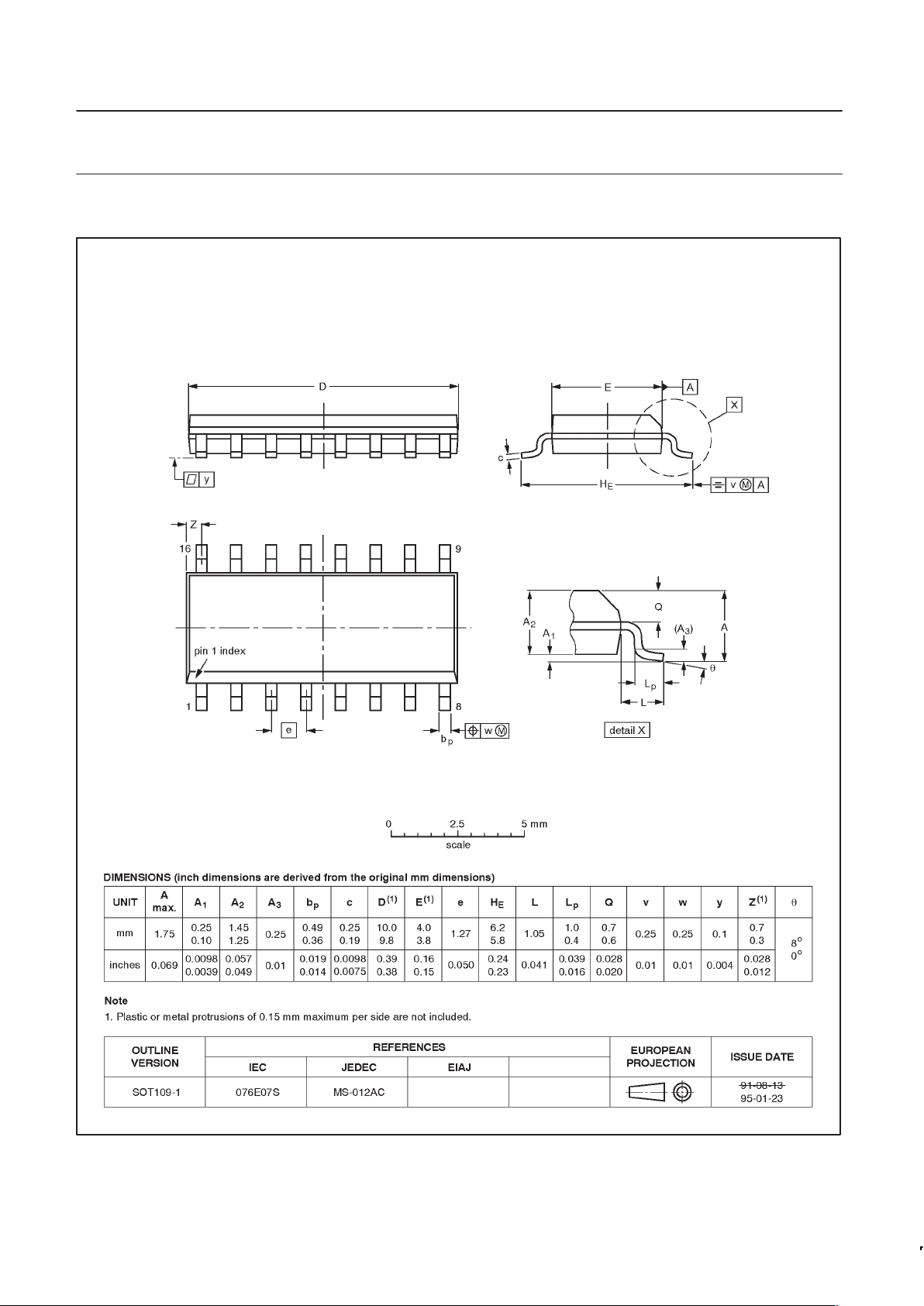
Philips Semiconductors Product specification
SA614ALow power FM IF system
1997 Nov 07
13
SO16: plastic small outline package; 16 leads; body width 3.9 mm SOT109-1
Page 14

Philips Semiconductors Product specification
SA614ALow power FM IF system
1997 Nov 07
14
Philips Semiconductors and Philips Electronics North America Corporation reserve the right to make changes, without notice, in the products,
including circuits, standard cells, and/or software, described or contained herein in order to improve design and/or performance. Philips
Semiconductors assumes no responsibility or liability for the use of any of these products, conveys no license or title under any patent, copyright,
or mask work right to these products, and makes no representations or warranties that these products are free from patent, copyright, or mask
work right infringement, unless otherwise specified. Applications that are described herein for any of these products are for illustrative purposes
only. Philips Semiconductors makes no representation or warranty that such applications will be suitable for the specified use without further testing
or modification.
LIFE SUPPORT APPLICA TIONS
Philips Semiconductors and Philips Electronics North America Corporation Products are not designed for use in life support appliances, devices,
or systems where malfunction of a Philips Semiconductors and Philips Electronics North America Corporation Product can reasonably be expected
to result in a personal injury. Philips Semiconductors and Philips Electronics North America Corporation customers using or selling Philips
Semiconductors and Philips Electronics North America Corporation Products for use in such applications do so at their own risk and agree to fully
indemnify Philips Semiconductors and Philips Electronics North America Corporation for any damages resulting from such improper use or sale.
This data sheet contains preliminary data, and supplementary data will be published at a later date. Philips
Semiconductors reserves the right to make changes at any time without notice in order to improve design
and supply the best possible product.
Philips Semiconductors
811 East Arques Avenue
P.O. Box 3409
Sunnyvale, California 94088–3409
Telephone 800-234-7381
DEFINITIONS
Data Sheet Identification Product Status Definition
Objective Specification
Preliminary Specification
Product Specification
Formative or in Design
Preproduction Product
Full Production
This data sheet contains the design target or goal specifications for product development. Specifications
may change in any manner without notice.
This data sheet contains Final Specifications. Philips Semiconductors reserves the right to make changes
at any time without notice, in order to improve design and supply the best possible product.
Copyright Philips Electronics North America Corporation 1997
All rights reserved. Printed in U.S.A.
 Loading...