

Page 1
Philips Semiconductors Linear Products Product specification
NE/SA594Vacuum fluorescent display driver
539
August 31, 1994 853-1045 13721
DESCRIPTION
The NE/SA594 is a display driver interface for vacuum fluorescent
displays. The device is comprised of 8 drivers and a bias network,
and is capable of driving the digits and/or segments of most vacuum
fluorescent displays.
The inputs are designed to be compatible with TTL, DTL, NMOS,
PMOS or CMOS output circuitry.
There is an active pull–down circuit on each output so that display
ghosting is minimized and no external components are required for
most fluorescent display applications.
FEATURES
•Digit and/or segment drivers
•Active output pull–down circuitry
•High output breakdown voltage
•Low supply voltage
•Input compatible with all logic outputs
APPLICATIONS
•Digital clocks
•Dashboard displays
•Panel displays
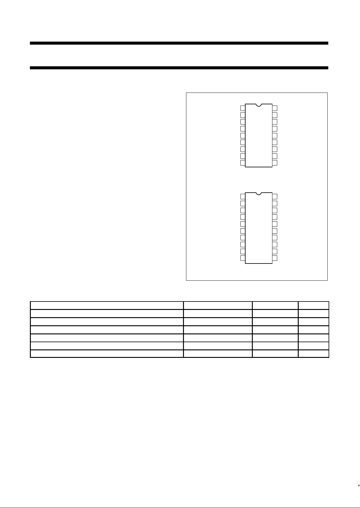
PIN CONFIGURATIONS
1
2
3
4
5
6
7
8
9
10
11
12
18
17
16
15
14
13
N, F Packages
TOP VIEW
1
2
3
4
5
6
7
8
9
10
11
12
13
14
20
19
18
17
16
15
D1 Package
TOP VIEW
NOTE:
1. SOL – Released in large SO package only.
IN 1
IN 2
IN 3
IN 4
IN 5
IN 6
IN 7
IN 8
GND
OUT 1
OUT 2
OUT 3
OUT 4
OUT 5
OUT 6
OUT 7
OUT 8
V+
IN 1
IN 2
IN 3
IN 4
IN 5
IN 6
IN 7
IN 8
GND
OUT 1
OUT 2
OUT 3
OUT 4
OUT 5
OUT 6
OUT 7
OUT 8
V+
NC
NC
ORDERING INFORMATION
DESCRIPTION TEMPERATURE RANGE ORDER CODE DWG #
18–Pin Plastic DIP 0 to +70°C NE594N 0407A
18–Pin Ceramic DIP 0 to +70°C NE594F 0583A
20–Pin Plastic SO 0 to +70°C NE594D 0408B
18–Pin Plastic DIP –40°C to +85°C SA594N 0407A
18–Pin Ceramic DIP –40°C to +85°C SA594F 0583A
20–Pin Plastic SO –40°C to +85°C SA594D 0408B
Page 2
Philips Semiconductors Linear Products Product specification
NE/SA594Vacuum fluorescent display driver
August 31, 1994
540
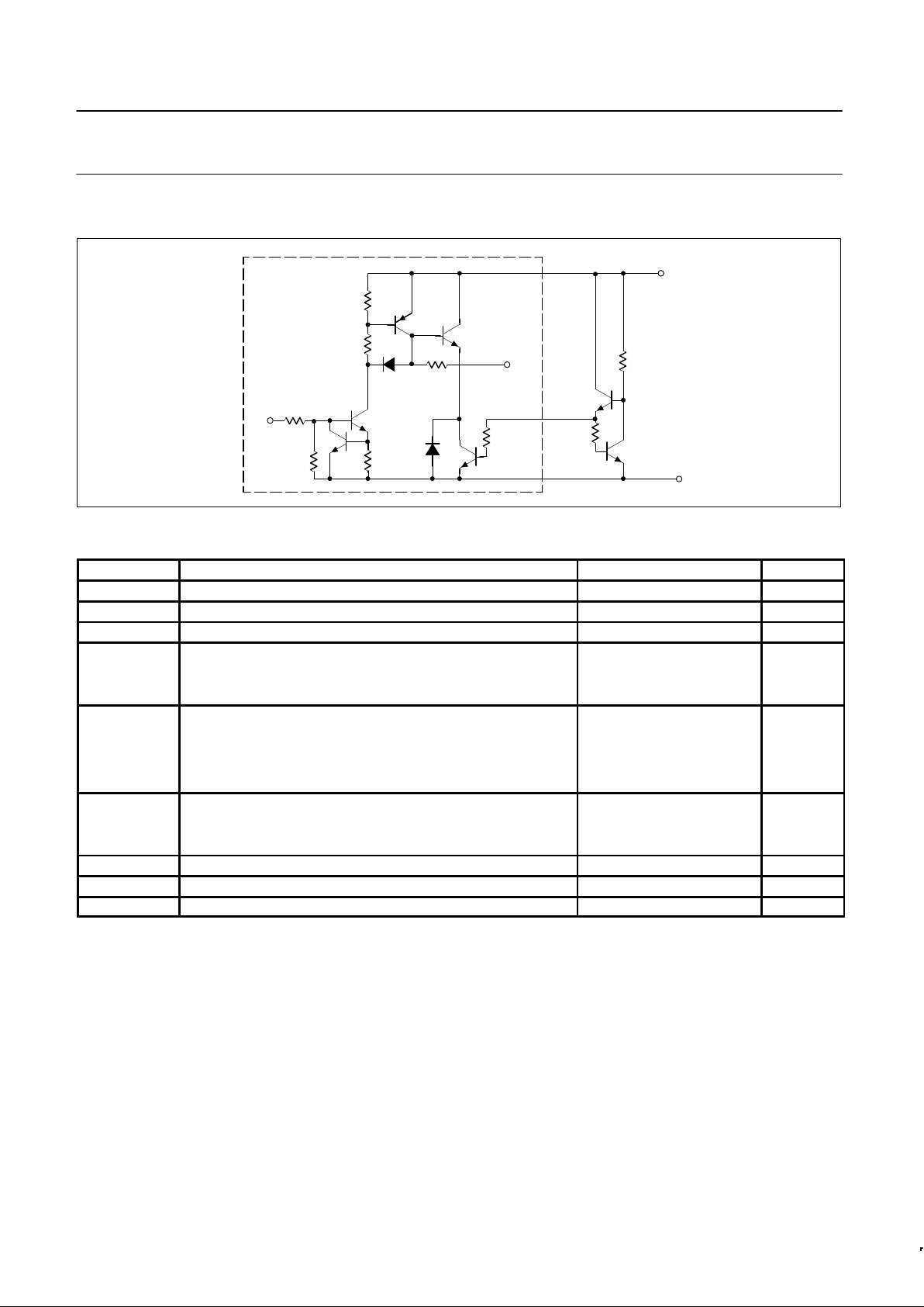
EQUIVALENT SCHEMATIC
I
N
R1
20K
R2
20K
X8
4.5K
R4
20K
R5
D1
Q3
R6
20K
Q4
OUT
Q2
Q1
R3
7.5K
D2
Q5
R7
10K
R8
10
K
Q7
Q6
R9
150
K
V
CC
GND
ABSOLUTE MAXIMUM RATINGS (at 25°C, unless otherwise noted)
SYMBOL
PARAMETER RATING UNIT
V
CC
Supply voltage 45 V
V
OUT
Output voltage V
CC
V
IN
Input voltage –0.3, +20 V
Output current
I
OUT
Each output 50 mA
All outputs 200 mA
Maximum power dissipation,
T
A
=25°C (still–air)
1
P
D
F package
N package
D package
1500
1690
1390
mW
mW
mW
Operating ambient temperature range
T
A
NE594 0 to 70 °C
SA594 –40 to +85 °C
T
STG
Storage temperature range +65 to +150 °C
T
J
Maximum junction temperature –150 °C
T
SOLD
Lead soldering temperature (10sec max) 300 °C
NOTES:
1. Derate above 25°C, at the following rates:
F package at 12.0mW/°C
N package at 13.5mW/°C
D package at 11.1mW/°C
Page 3

Philips Semiconductors Linear Products Product specification
NE/SA594Vacuum fluorescent display driver
August 31, 1994
541
DC ELECTRICAL CHARACTERISTICS
VCC=+4.75 to +40V, TA=0 to 70°C (NE), TA= –40 to +85°C (SA), unless otherwise stated.
LIMITS
SYMBOL
PARAMETER
TEST CONDITIONS
Min Typ Max
UNIT
V
CC
Supply voltage range 4.75 35 40 V
I
CCH
Supply current (all outputs high) VCC=40V, VIN=3.5V 3 6 mA
I
CCL
Supply current (all outputs low) VCC=40V, VIN=0.4V 0.4 1 mA
V
IN
Input voltage range 0 15 V
V
IH
Input voltage to ensure logic ”1’ 2.6 V
V
IL
Input voltage to ensure logic ”0’ 0.8 V
I
IH
Input current to ensure logic ”1’ 100 µA
I
IL
Input current to ensure logic ”0’ 10 µA
I
IN
Input current VIN=2.6V 60 130 µA
VIN=5.0V 180 330 µA
VIN=15.0V .68 1.3 mA
V
OH
Output high voltage
VIN=3.5V
I
OUT
=–25mA
TA=25°C VCC–1.5 VCC–1.1 V
Over temp. VCC–2 VCC–1.3 V
V
OUT
with respect
to V
CC
V
OH
Output high, no load voltage
VIN=3.5V,
I
OUT
=0, TA=25°C,
V
OUT
with respect to V
CC
VCC–1 VCC–0.8 V
V
OFF
Output ‘OFF’ voltage level
VIN=0.8V,
I
OUT
=0
10 200 mV
I
OH
Available output current
VCC=35V, VIN=3.5V,
V
OUT
=30V, TA=25°C
–35 mA
I
OUT
Output pull-down current
VCC=V
OUT
=35V,
Inputs open
100 200 400 µA
I
CEX
Output leakage current
TA=25°C, VIN=0.4V
V
CC
=40V, V
OUT
=0V
–1
–1
µA
AC ELECTRICAL CHARACTERISTICS
VCC=35V, TA=25°C
LIMITS
SYMBOL
PARAMETER
TEST CONDITIONS
Min Typ Max
UNIT
t
PLH
Propagation delay—low–to–high output transition 50% VIN to 50% V
OUT
1 5 µs
t
PHL
Propagation delay—high–to–low output transition 50% VIN to 50% V
OUT
3 10 µs
t
R
Output rise time 10% V
OUT
to 90% V
OUT
0.5 3 µs
t
F
Output fall time 90% V
OUT
to 10% V
OUT
1.5 5 µs
Page 4

Philips Semiconductors Linear Products Product specification
NE/SA594Vacuum fluorescent display driver
August 31, 1994
542
SWITCHING TIMES OF DRIVERS
5V
0
V
IN
34V
V
OUT
90%
50%
10%
t
PDLH
0V
P
RR
t
PDLH
10%
50%
90%
t
R
t
F
P
RR
tFt
F
Figure 1. Test Circuit
V
IN
P
RR = 10kHz
tR = tF = (50ns)
V
cc
= 35V
R
L
C
L
RL = 10kΩ
C
L
= 50pF
V
OUT
Page 5

Philips Semiconductors Linear Products Product specification
NE/SA594Vacuum fluorescent display driver
August 31, 1994
543
TYPICAL PERFORMANCE CHARACTERISTICS
V
OUT
(V)
IIN vs V
IN
I
CCH
vs Temperature
Output Voltage vs Output Current I
CC
vs VCC (All inputs High)
1000
800
600
400
200
0
0 5 10 15 20
I
IN
(µA)
V
IN
(V)
V
CC = 40V
I
CCH
(mA)
TEMPERATURE
o
C
5
4
3
2
1
0
–40 0 25 50 85
V
CC
V
CC
V
CC
V
CC
V
CC
V
CC
–1
–2
–3
–4
–5
0 10 20 30 40 50
I
OUT
(mA)
T
A =
25
o
C
T
A =
25
o
C
5
4
3
2
1
0
0 10 20 30 40 50
V
CC
(V)
I
CCH
(mA)
Page 6

Philips Semiconductors Linear Products Product specification
NE/SA594Vacuum fluorescent display driver
August 31, 1994
544
2N222
O
C
1/2
LM393
R9
15K
Figure 2. Typical Application: Digital Clock With Alarm
T
1
40V
RMS
1N4002
+
0.47µF
2
78mG
R7
5.6K
R8
50K
DIMMER
ADJUST
4
1N914
.1µF
ALARM
SET
N.O.
HOUR
SET
N.O.
MIN
SET
N.O.
10
+12V
R1
100K
R4
100K
R5
1 MEG
4
5
1/2
LM393
+12V
R3
10K
6
2
3
+12V
8
1
R2
10K
7
5.6Ω 1
W
5.6Ω 1
W
Z, 5.6V
IN 752
+V
10 11
9 8
F
I
L
12
A
M
S
E
G
A/P
D
I
G
I
T
A
M
S
E
G
A
S
E
G
7
L
S
E
G
D
S
E
G
10
HR
D
I
G
I
T
10
HR
D
I
G
I
T
S
H
I9
E
L
D
ITRON JJA
CLOCK DISPLAY
6 5 4 3 2
13 14 15 16 17 18
+12V
28
6
5
1
7
8
27
9
24
4
2
26
+V
NE/SA594
+ V + 16 TO + 40V
78
HV12
1
2
3
22
11
12
ALARM
OFF
ALARM
ENABLE
N.C.
N.O.
SNOOZE
Q1
R6
100Ω
8Ω
NE/SA594
9 8 7 6 5 4 3 2
10 11 12 13 14 15 16 17 18
S
GC
O
L
10
MIN
D
I
G
C
S
E
G
1
MIN
D
I
G
E
S
EGE
G
F
S
E
G
B
S
E
G
F
I
L
O
N
DIITI
T
I
T
G
13
14
15
23
18
19
17
25
3
MK
50250
T
2
 Loading...