

Page 1
查询AU5232供应商查询AU5232供应商
INTEGRATED CIRCUITS
NE/SA/AU5232
Matched dual high-performance
low-voltage operational amplifier
Product data 2002 May 21
Page 2
Philips Semiconductors Product data
Matched dual high-performance
low-voltage operational amplifier
DESCRIPTION
The NE/SA/AU5232 is a matched, low voltage, high performance
dual operational amplifier . Among its unique input and output
characteristics is the capability for both input and output rail-to-rail
operation, particularly critical in low voltage applications. The output
swings to less than 50 mV of both rails across the entire power
supply range. The NE/SA/AU5232 is capable of delivering 5.5 V
peak-to-peak across a 600 Ω load and will typically draw only
700 µA per amplifier. The bandwidth is 2.5 MHz and the 1% settling
time is 1.4 µs.
FEATURES
•Wide common-mode input voltage range: 250 mV beyond both
rails
•Output swing within 50 mV of both rails
•Functionality to 1.8 V typical
•Low current consumption: 700 µA per amplifier
•±15 mA output current capability
•Unity gain bandwidth: 2.5 MHz
•Slew rate: 0.8 V/µs
•Low noise: 33 nV/√Hz
•Electrostatic discharge protection
•Short-circuit protection
•Output inversion prevention
NE/SA/AU5232
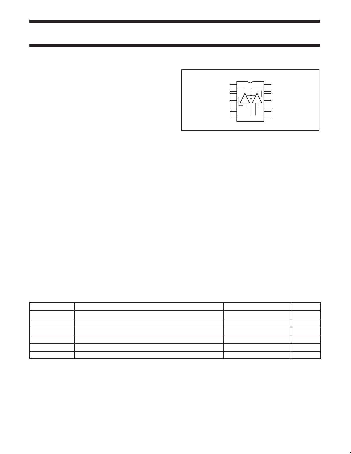
PIN CONFIGURATION
D, N Packages
OUTPUT A
INVERTING INPUT A
NON INVERTING INPUT A
1
2
AB
–+
3
V–
45
Figure 1. Pin configuration.
APPLICATIONS
•Automotive electronics
•Signal conditioning and sensing amplification
•Portable instrumentation
– Test and measurement
– Medical monitors and diagnostics
– Remote meters
•Audio equipment
•Security systems
•Communications
– Pagers
– Cellular telephone
– LAN
– 5 V Datacom bus
•Error amplifier in motor drives
•Transducer buffer amplifier
+
–
SL01163
8
7
6
V+
OUTPUT B
INVERTING INPUT B
NON INVERTING INPUT B
ORDERING INFORMATION
ORDER CODE DESCRIPTION TEMPERATURE RANGE DWG #
NE5232D 8-Pin Plastic Small Outline (SO) package 0 °C to +70 °C SOT96-1
NE5232N 8-Pin Plastic Dual In-Line Package (DIP) 0 °C to +70 °C SOT97-1
SA5232D 8-Pin Plastic Small Outline (SO) package –40 °C to +85 °C SOT96-1
SA5232N 8-Pin Plastic Dual In-Line Package (DIP) –40 °C to +85 °C SOT97-1
AU5232N 8-Pin Plastic Dual In-Line Package (DIP) –40 °C to +125 °C SOT97-1
AU5232D 8-Pin Plastic Small Outline (SO) package –40 °C to +125 °C SOT96-1
2002 May 21 853–2347 28261
2
Page 3
Philips Semiconductors Product data
T
b
Matched dual high-performance
low-voltage operational amplifier
ABSOLUTE MAXIMUM RATINGS
SYMBOL PARAMETER RATING UNIT
V
CC
V
ESD
V
S
V
DP
I
DP
V
i(dif)
V
i(CM)
V
i(CM)
P
D
T
j
V
SC
T
stg
T
sld
θ
JA
NOTES:
1. Each pin is protected by ESD diodes. The voltage at any pin is limited by the ESD diodes.
2. The differential input of each amplifier is limited by two internal diodes, connected in parallel and opposite to each other. For more differential
input range, use differential resistors in series with the input pins.
3. The maximum operating junction temperature is +150 °C. At elevated temperatures, devices must be derated according to the package
thermal resistance and device mounting conditions. Derates above +25 °C: N package at 9.5 mW/°C; D package at 6.25 mW/°C.
4. Simultaneous short circuits of two amplifiers to the positive or negative rail can exceed the power dissipation ratings and cause eventual
destruction of the device.
5. Guaranteed by design.
Single supply voltage 7 V
ESD protection voltage at any pin
5
human body model 2000 V
robot model 200 V
Dual supply voltage ±3.5 V
Voltage at any device pin
Current into any device pin
Differential input voltage
1
1
2
VS ± 0.5 V
Common-mode input voltage (positive) VCC + 0.5 V
Common-mode input voltage (negative) VEE – 0.5 V
Power dissipation
Operating junction temperature
Supply voltage allowing indefinite output short circuit to either rail
3
3
3,4
Storage temperature range –65 to +150 °C
Lead soldering temperature (10 sec max) +230 °C
Thermal impedance
8-pin plastic DIP °C/W
8-pin plastic SO °C/W
NE/SA/AU5232
±50 mA
0.5 V
500 mW
+150 °C
7 V
RECOMMENDED OPERATING CONDITIONS
SYMBOL PARAMETER RATING UNIT
V
V
V
CC
V
i(CM)
i(CM)
am
S
Single supply voltage +2 to +5.5 V
Dual supply voltage ±1 to ±2.75 V
Common-mode input voltage (positive) VCC + 0.25 V
Common-mode input voltage (negative) VEE – 0.25 V
Temperature
NE 0 to +70 °C
SA –40 to +85 °C
AU –40 to +125 °C
2002 May 21
3
Page 4

Philips Semiconductors Product data
VOSOffset voltage
mV
∆V
y
mV
IOSOffset current
nA
IBInput bias current
1
nA
amplifier in the same
nA
ackage at the same
l
j
PSRR
yj
dB
I
,
mA
A
Open-loop voltage gain
dB
Out ut voltage swing
V
gg
V
Matched dual high-performance
low-voltage operational amplifier
DC ELECTRICAL CHARACTERISTICS
VCC = 2 V to 5.5 V, VEE = 0 V, T
SYMBOL PARAMETER
I
∆VOS/∆T
Supply current
CC
Offset voltage drift with
temperature
Offset voltage difference
between any amplifiers in
OS
the same package at the
same common mode level
∆IOS/∆T
Offset current drift with
temperature
p
∆IB/∆T
Input bias current drift with
temperature
Input bias current
∆I
difference between any
B
p
package at the same
common mode level.
V
i(CM)
Common-mode input range
Common-mode rejection
CMRR
ratio, small signa
Common-mode rejection
ratio, large signal
Power supply rejection
ratio
Peak load current, sink and
L
source
p
VOL
p
p
V
OUT
Output voltage swing for
VCC = 2.75 V , VEE = –2.75 V
NOTE:
1. These parameters are measured for V
for common mode ranges between the measured regions.
= 25 °C; VEE < V
amb
1
VEE < V
VEE < V
VEE < V
EE
TEST CONDITIONS
VCC = 5.5V 1.4 2.0 1.4 2.0
VCC = 5.5 V;
over full temp. range
Over full temp. range ±0.4 ±5 ±0.6 ±5
Over full temp. range 0.8 4 1.2 4
Over full temp. range ±4 ±30 ±6 ±60
i(CM)
Over full temp. range –225 –100 –250 –150
VEE +1 V < V
Over full temp. range 35 100 35 120
i(CM)
Over full temp. range 25 50 50 70
VEE +1 V < V
Over full temp. range 15 30 25 50
VOS ≤ 6 mV VEE–0.25 VCC+0.25 VEE–0.25 VCC+0.25
VOS ≤ 6 mV;
Over full temp. range
i(CM)
VEE+1V < V
Over full temp. range 75 100 75
VEE < V
Over full temp. range 60 80 60
VEE < V
Over full temp. range 80 90 80 90
Over full temp. range 5 8 5 8
Over full temp. range 90 90
I
PEAK
I
PEAK
I
PEAK
over full temp. range
RL = 2 kΩ VEE+0.2 VCC–0.2 VEE+0.2 VCC–0.2
RL = 600 Ω VEE+0.25 VCC–0.25 VEE+0.25 VCC–0.25
< VCM < VEE+0.5 V and for VEE+1 V < VCM < VCC. By design these parameters are intermediate
NE/SA/AU5232
< VCC; unless otherwise stated.
i(CM)
LIMITS
NE5232 SA5232
MIN TYP MAX MIN TYP MAX
1.5 2.3 1.6 2.4
±0.2 ±4 ±0.2 ±4
4 4 µV/°C
0.4 3 0.4 3
±3 ±20 ±3 ±30
0.02 ±.3 0.03 ±.3 nA/°C
< VEE +0.5 V –200 –90 –200 –90
< V
i(CM)
CC
< VEE +0.5 V 10 30 10 30
< V
i(CM)
CC
VEE–0.1 VCC+0.1 VEE–0.1 VCC+0.1
< VEE+0.5V;
< V
i(CM)
< V
i(CM)
CC
< V
i(CM)
CC
CC
80 100 80 100
65 90 65 90
80 100 80 100
10 12 10 12
90 110 90 110
= 0.1 mA VEE+0.05 VCC–0.05 VEE+0.1 VCC–0.1
= 10 mA VEE+0.25 VCC–0.25 VEE+0.25 VCC–0.25
= 5 mA;
VEE+0.22 VCC–0.22 VEE+0.2 VCC–0.2
25 70 25 75
0.5 0.5 nA/°C
5 20 5 20
UNIT
mA
V
dB
2002 May 21
4
Page 5

Philips Semiconductors Product data
VOSOffset voltage
mV
∆V
gy
mV
IOSOffset current
nA
IBInput bias current
1
nA
y
nA
j,g
Common-mode rejection ratio, large signal
PSRR
Power supply rejection ratio
dB
ILPeak load current, sink and source
mA
A
Open-loop voltage gain
dB
Out ut voltage swing
V
gg
V
Matched dual high-performance
low-voltage operational amplifier
DC ELECTRICAL CHARACTERISTICS
VCC = 2 V to 5.5 V, VEE = 0 V, T
SYMBOL PARAMETER
I
CC
Supply current
∆VOS/∆T Offset voltage drift with temperature 4 µV/°C
Offset voltage difference between any amplifiers in the
OS
same package at the same common mode level
∆IOS/∆T Of fset current drift with temperature 0.03 ±.3 nA/°C
p
∆IB/∆T Input bias current drift with temperature 0.5 nA/°C
∆I
B
Input bias current difference between any amplifier in the
same package at the same common mode level.
V
i(CM)
Common-mode input range
Common-mode rejection ratio, small signal
CMRR
pp
p
VOL
p
p
V
OUT
Output voltage swing for
VCC = 2.75 V , VEE = –2.75 V
NOTE:
1. These parameters are measured for V
for common mode ranges between the measured regions.
= 25 °C; VEE < V
amb
EE
< VCC; unless otherwise stated.
i(CM)
TEST CONDITIONS
VCC = 5.5V 1.4 2.0
VCC = 5.5 V;
over full temp. range
Over full temp. range ±0.6 ±5
1
Over full temp. range 1.2 4
Over full temp. range ±6 ±60
VEE < V
< VEE +0.5 V –200 –90
i(CM)
Over full temp. range –250 –150
VEE +1 V < V
i(CM)
< V
CC
Over full temp. range 35 120
VEE < V
< VEE +0.5 V 10 30
i(CM)
Over full temp. range 50 70
VEE +1 V < V
i(CM)
< V
CC
Over full temp. range 25 50
VOS ≤ 6 mV VEE–0.25 VCC+0.25
VOS ≤ 6 mV;
Over full temp. range
VEE < V
VEE+1V < V
< VEE+0.5V;
i(CM)
i(CM)
< V
VEE–0.1 VCC+0.1
CC
Over full temp. range 70
VEE < V
i(CM)
< V
CC
Over full temp. range 55
VEE < V
i(CM)
< V
CC
Over full temp. range 75 90
Over full temp. range 5 8
Over full temp. range 90
I
= 0.1 mA VEE+0.1 VCC–0.1
PEAK
I
= 10 mA VEE+0.25 VCC–0.25
PEAK
I
= 5 mA;
PEAK
over full temp. range
VEE+0.2 VCC–0.2
RL = 2 kΩ VEE+0.2 VCC–0.2
RL = 600 Ω VEE+0.25 VCC–0.25
< VCM < VEE+0.5 V and for VEE+1 V < VCM < VCC. By design these parameters are intermediate
NE/SA/AU5232
LIMITS
AU5232
MIN TYP MAX
1.6 2.4
±0.2 ±4
0.4 3
±3 ±30
25 75
5 20
80 100
65 90
80 100
10 12
90 110
UNIT
mA
V
dB
2002 May 21
5
Page 6

Philips Semiconductors Product data
Matched dual high-performance
low-voltage operational amplifier
AC ELECTRICAL CHARACTERISTICS
T
= +25 °C; VCC = 2 V to 5.5 V; RL = 10 kΩ; CL = 100 pF; unless otherwise stated.
amb
LIMITS
SYMBOL P ARAMETER TEST CONDITIONS
SR Slew rate Over full temperature range 0.5 0.8 0.5 0.8 V/µs
BW Unity gain bandwidth: –3 dB Over full temperature range 2 2.5 4.0 2 2.5 4.0 MHz
θ
Phase Margin CL = 50 pF 55 55 deg
M
t
1% settling time AV = 1, 1 V step 1.4 1.4 µs
S
V
THD Total harmonic distortion 10 kHz, 1V
Input referred voltage noise AV = 1, RS = 0 Ω, at 1 kHz 33 33 nV/Hz
N
, AV = 1 0.1 0.1 %
P-P
OUTPUT INVERSION PREVENTION
V
5 V
IN
V
CC
V
GND
CONVENTIONAL OP AMP PHILIPS NE5232
V
OUT
47 kΩ
V
t
IN
47 kΩ
Figure 2. Output inversion prevention.
V
CC
+
–
NE5232 SA/AU5232
MIN TYP MAX MIN TYP MAX
V
OUT
V
GND
NE/SA/AU5232
V
IN
V
OUT
t
UNIT
V
CC
5 V
V
GND
SL01617
1/2
2002 May 21
6
Page 7

Philips Semiconductors Product data
Matched dual high-performance
low-voltage operational amplifier
SO8: plastic small outline package; 8 leads; body width 3.9 mm SOT96-1
NE/SA/AU5232
2002 May 21
7
Page 8

Philips Semiconductors Product data
Matched dual high-performance
low-voltage operational amplifier
DIP8: plastic dual in-line package; 8 leads (300 mil) SOT97-1
NE/SA/AU5232
2002 May 21
8
Page 9

Philips Semiconductors Product data
Matched dual high-performance
low-voltage operational amplifier
NE/SA/AU5232
NOTES
2002 May 21
9
Page 10

Philips Semiconductors Product data
Matched dual high-performance
low-voltage operational amplifier
Data sheet status
Product
Data sheet status
Objective data
Preliminary data
Product data
[1] Please consult the most recently issued data sheet before initiating or completing a design.
[2] The product status of the device(s) described in this data sheet may have changed since this data sheet was published. The latest information is available on the Internet at URL
http://www.semiconductors.philips.com.
[1]
status
Development
Qualification
Production
[2]
Definitions
Short-form specification — The data in a short-form specification is extracted from a full data sheet with the same type number and title. For
detailed information see the relevant data sheet or data handbook.
Limiting values definition — Limiting values given are in accordance with the Absolute Maximum Rating System (IEC 60134). Stress above one
or more of the limiting values may cause permanent damage to the device. These are stress ratings only and operation of the device at these or
at any other conditions above those given in the Characteristics sections of the specification is not implied. Exposure to limiting values for extended
periods may affect device reliability.
Application information — Applications that are described herein for any of these products are for illustrative purposes only. Philips
Semiconductors make no representation or warranty that such applications will be suitable for the specified use without further testing or
modification.
Disclaimers
Life support — These products are not designed for use in life support appliances, devices or systems where malfunction of these products can
reasonably be expected to result in personal injury . Philips Semiconductors customers using or selling these products for use in such applications
do so at their own risk and agree to fully indemnify Philips Semiconductors for any damages resulting from such application.
Right to make changes — Philips Semiconductors reserves the right to make changes, without notice, in the products, including circuits, standard
cells, and/or software, described or contained herein in order to improve design and/or performance. Philips Semiconductors assumes no
responsibility or liability for the use of any of these products, conveys no license or title under any patent, copyright, or mask work right to these
products, and makes no representations or warranties that these products are free from patent, copyright, or mask work right infringement, unless
otherwise specified.
Contact information
For additional information please visit
http://www.semiconductors.philips.com . Fax: +31 40 27 24825
For sales offices addresses send e-mail to:
sales.addresses@www.semiconductors.philips.com.
Definitions
This data sheet contains data from the objective specification for product development.
Philips Semiconductors reserves the right to change the specification in any manner without notice.
This data sheet contains data from the preliminary specification. Supplementary data will be
published at a later date. Philips Semiconductors reserves the right to change the specification
without notice, in order to improve the design and supply the best possible product.
This data sheet contains data from the product specification. Philips Semiconductors reserves the
right to make changes at any time in order to improve the design, manufacturing and supply.
Changes will be communicated according to the Customer Product/Process Change Notification
(CPCN) procedure SNW-SQ-650A.
Koninklijke Philips Electronics N.V. 2002
Document order number: 9397 750 09837
NE/SA/AU5232
All rights reserved. Printed in U.S.A.
Date of release: 06-02
2002 May 21
10
 Loading...