

Page 1
DATA SHEET
HETERO JUNCTION FIELD EFFECT TRANSISTOR
NE32500, NE27200
C to Ka BAND SUPER LOW NOISE AMPLIFIER
N-CHANNEL HJ-FET CHIP
DESCRIPTION
NE32500 and NE27200 are Hetero Junction FET chip that utilizes the hetero junction between Si-doped AlGaAs
and undoped InGaAs to create high mobility electrons. Its excellent low noise and high associated gain make it suitable
for commercial systems, industrial and space applications.
FEATURES
• Super Low Noise Figure & High Associated Gain
NF = 0.45 dB TYP., Ga = 12.5 dB TYP. at f = 12 GHz
• Gate Length : L
• Gate Width : Wg = 200 µm
g = 0.2
µ
m
ORDERING INFORMATION
PART NUMBER QUALITY GRADE
NE32500 Standard (Grade D)
NE27200 Special, specific (Grade C and B)
ABSOLUTE MAXIMUM RATINGS (TA = 25 ˚C)
Drain to Source Voltage VDS 4.0 V
Gate to Source Voltage V
Drain Current ID IDSS mA
Total Power Dissipation Ptot* 200 mW
Channel Temperature T
Storage Temperature Tstg –65 to +175 °C
* Chip mounted on a Alumina heatsink (size: 3 × 3 × 0.6t)
GS –3.0 V
ch 175 °C
ELECTRICAL CHARACTERISTICS (TA = 25 ˚C)
PARAMETER SYMBOL MIN. TYP. MAX. UNIT TEST CONDITIONS
Gate to Source Leak Current IGSO – 0.5 10
Saturated Drain Current IDSS 20 60 90 mA VDS = 2 V, VGS = 0 V
Gate to Source Cutoff Voltage VGS(off) –0.2 –0.7 –2.0 V VDS = 2 V, ID = 100 µA
Transconductance gm 45 60 – mS VDS = 2 V, ID = 10 mA
Thermal Resistance Rth* – – 260 ˚C/W channel to case
Noise Figure NF – 0.45 0.55 dB VDS = 2 V, ID = 10 mA, f = 12 GHz
Associated Gain Ga 11.0 12.5 – dB
µ
AVGS = –3 V
RF performance is determined by packaging and testing 10 chips per wafer.
Wafer rejection criteria for standard devices is 2 rejects per 10 samples.
Document No. P11512EJ2V0DS00 (2nd edition)
Date Published January 1997 N
Printed in Japan
©
1996
Page 2
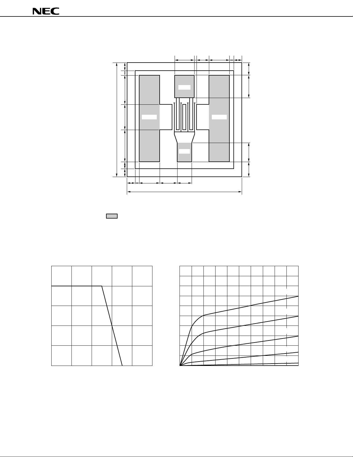
CHIP DIMENSIONS (Unit: µm)
5.5 13
58 36.5 66 25
NE32500, NE27200
2589
13
350
25 21 76.5100.5
Thickness = 140 m
: BONDING AREA
Source Source
25 49.5 4366
13
µ
Drain
Gate
350
38
686046.5
TYPICAL CHARACTERISTICS (TA = 25 ˚C)
TOTAL POWER DISSIPATION vs.
AMBIENT TEMPERATURE
250 100
200
150
100
50
– Total Power Dissipation – mW
tot
P
0050 1.5 3.0100 150 200 250
T
A
– Ambient Temperature – ˚C VDS – Drain to Source Voltage – V
DRAIN CURRENT vs.
DRAIN TO SOURCE VOLTAGE
80
60
40
– Drain Current – mA
D
I
20
VGS = 0 V
–0.2 V
–0.4 V
–0.6 V
–0.8 V
2
Page 3
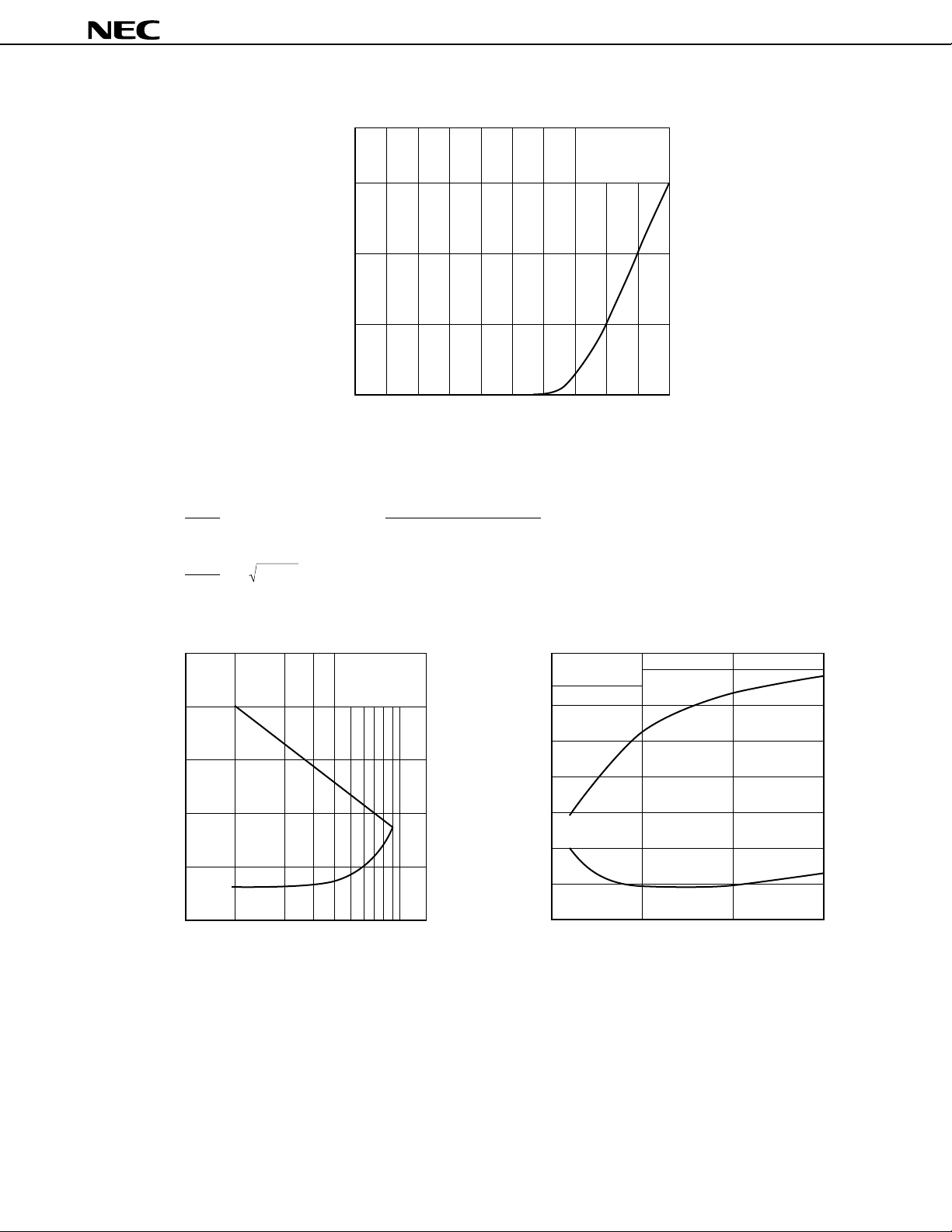
DRAIN CURRENT vs.
GATE TO SOURCE VOLTAGE
60
40
– Drain Current – mA
D
20
I
V
DS
NE32500, NE27200
= 2 V
Gain Calculations
||
S
MSG. =
MAG.
21
12
||
S
|S |
21
12
|S |
(K K 1)
=±−
NOISE FIGURE, ASSOCIATED GAIN vs.
FREQUENCY
Ga
1.0
0
–1.0–2.0 0
GS
– Gate to Source Voltage – V
V
2
1 | | |S | |S |
+− −
K
2
∆
∆
=
2|S ||S |
=⋅−⋅SS SS11 22 21 12
2
11
12 21
2
22
NOISE FIGURE, ASSOCIATED GAIN vs.
DRAIN CURRENT
V
DS = 2 V
I
D = 10 mA
24
20
V
DS = 2 V
f = 12 GHz
14
G
a
13
12
16
11
10
12
2.0
1.5
NF – Noise Figure – dB
0.5
a – Associated Gain – dB
G
8
1.0
NF – Noise Figure – dB
0.5
NF
0
1246810142030 10020
4
f – Frequency – GHz I
NF
30
D – Drain Current – mA
a – Associated Gain – dB
G
3
Page 4
NE32500, NE27200
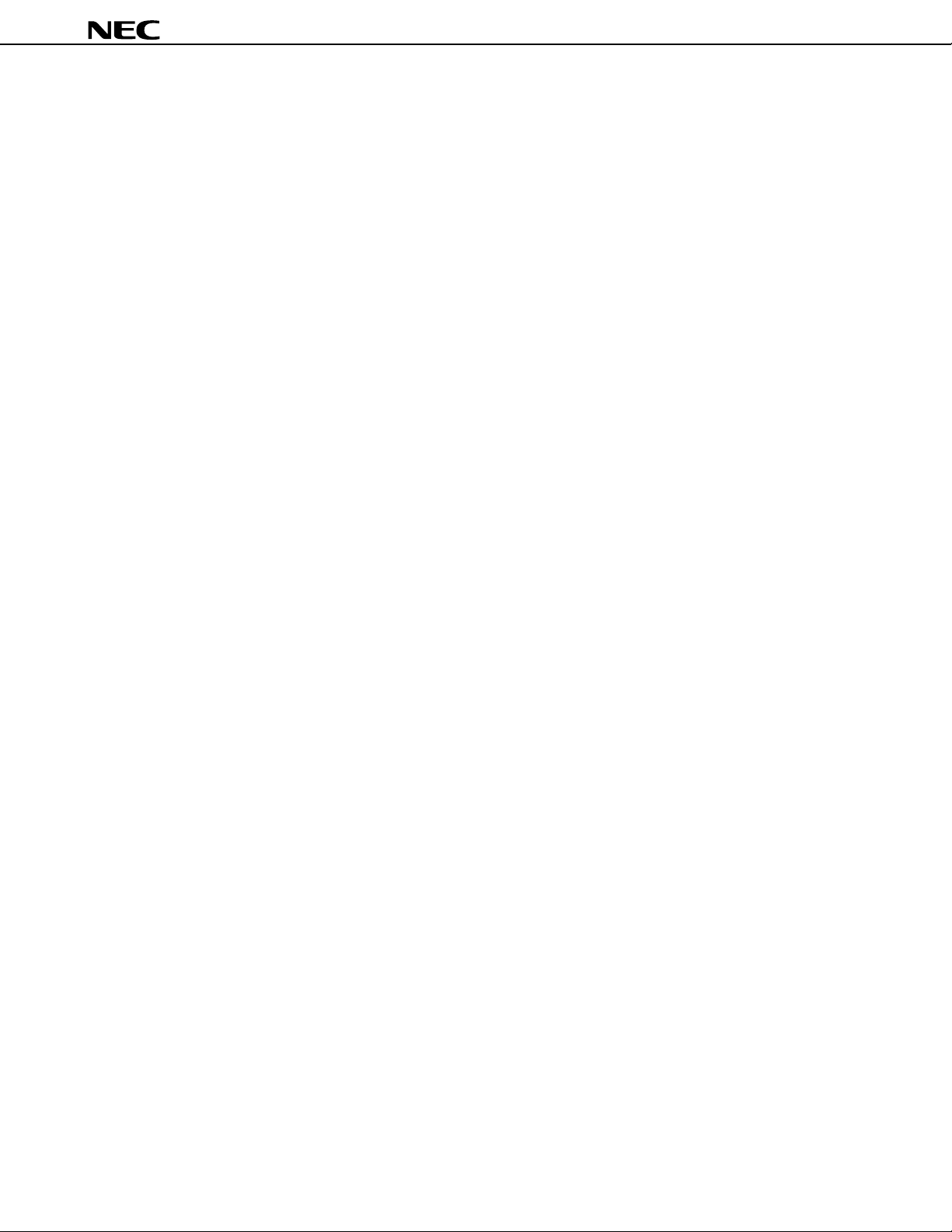
S-PARAMETERS MAG. AND ANG.
VDS = 2 V, ID = 10 mA
FREQUENCY S11 S21 S12 S22
MAG. ANG. MAG. ANG. MAG. ANG. MAG. ANG.
(MHz) (deg.) (deg.) (deg.) (deg.)
500 0.999 –4 4.34 177 0.006 82 0.564 –3
1000 0.998 –7 4.33 174 0.012 84 0.562 –6
2000 0.996 –14 4.28 168 0.025 81 0.559 –11
3000 0.992 –20 4.26 163 0.037 76 0.557 –17
4000 0.976 –28 4.24 158 0.048 71 0.551 –23
5000 0.962 –36 4.11 152 0.060 66 0.546 –29
6000 0.962 –42 4.06 148 0.070 62 0.539 –34
7000 0.943 –48 3.95 143 0.079 58 0.533 –40
8000 0.928 –55 3.83 139 0.087 55 0.526 –44
9000 0.920 –60 3.73 134 0.095 51 0.519 –49
10000 0.900 –67 3.58 129 0.104 47 0.508 –54
11000 0.881 –72 3.46 126 0.109 43 0.503 –58
12000 0.869 –77 3.34 122 0.114 40 0.494 –62
13000 0.856 –82 3.23 118 0.120 37 0.488 –66
14000 0.839 –86 3.11 115 0.123 34 0.483 –69
15000 0.831 –91 3.01 112 0.127 32 0.476 –72
16000 0.818 –96 2.88 108 0.131 29 0.472 –76
17000 0.804 –99 2.78 105 0.134 27 0.468 –79
18000 0.796 –103 2.68 103 0.137 24 0.464 –81
19000 0.784 –106 2.59 100 0.141 22 0.460 –84
20000 0.782 –111 2.49 96 0.142 20 0.456 –88
21000 0.772 –114 2.42 95 0.144 19 0.457 –90
22000 0.761 –117 2.33 93 0.147 17 0.450 –92
23000 0.758 –119 2.25 90 0.147 15 0.454 –94
24000 0.753 –122 2.20 88 0.148 14 0.453 –95
25000 0.748 –125 2.11 86 0.150 12 0.453 –98
26000 0.746 –127 2.06 84 0.152 11 0.460 –100
27000 0.750 –129 2.01 82 0.154 9 0.453 –101
28000 0.738 –133 1.93 79 0.151 7 0.453 –104
29000 0.744 –135 1.90 77 0.153 7 0.453 –105
30000 0.742 –138 1.84 75 0.156 4 0.454 –107
4
Page 5
NE32500, NE27200
CHIP HANDLING
DIE ATTACHMENT
Die attach operation can be accomplished with Au-Sn (within a 300 ˚C – 10 s) performs in a forming gas
environment.
Epoxy die attach is not recommend.
BONDING
Bonding wires should be minimum length, semi hard gold wire (3-8 % elongation) 20 microns in diameter.
Bonding should be performed with a wedge tip that has a taper of approximately 15 %. Bonding time should be
kept to minimum.
As a general rule, the bonding operation should be kept within a 280 ˚C, 2 minutes for all bonding wires.
If longer periods are required, the temperature should be lowered.
PRECAUTIONS
The user must operate in a clean, dry environment. The chip channel is glassivated for mechanical protection only
and does not preclude the necessity of a clean environment.
The bonding equipment should be periodically checked for sources of surge voltage and should be properly
grounded at all times. In fact, all test and handling equipment should be grounded to minimize the possibilities of static
discharge.
Avoid high static voltage and electric fields, because this device is Hetero Junction field effect transistor with shottky
barrier gate.
CAUTION
The Great Care must be taken in dealing with the devices in this guide.
The reason is that the material of the devices is GaAs (Gallium Arsenide), which is
designated as harmful substance according to the law concerned.
Keep the law concerned and so on, especially in case of removal.
5
Page 6
[MEMO]
NE32500, NE27200
6
Page 7
[MEMO]
NE32500, NE27200
7
Page 8
NE32500, NE27200
No part of this document may be copied or reproduced in any form or by any means without the prior written
consent of NEC Corporation. NEC Corporation assumes no responsibility for any errors which may appear in
this document.
NEC Corporation does not assume any liability for infringement of patents, copyrights or other intellectual property
rights of third parties by or arising from use of a device described herein or any other liability arising from use
of such device. No license, either express, implied or otherwise, is granted under any patents, copyrights or other
intellectual property rights of NEC Corporation or others.
While NEC Corporation has been making continuous effort to enhance the reliability of its semiconductor devices,
the possibility of defects cannot be eliminated entirely. To minimize risks of damage or injury to persons or
property arising from a defect in an NEC semiconductor device, customers must incorporate sufficient safety
measures in its design, such as redundancy, fire-containment, and anti-failure features.
NEC devices are classified into the following three quality grades:
"Standard", "Special", and "Specific". The Specific quality grade applies only to devices developed based on a
customer designated "quality assurance program" for a specific application. The recommended applications of
a device depend on its quality grade, as indicated below. Customers must check the quality grade of each device
before using it in a particular application.
Standard: Computers, office equipment, communications equipment, test and measurement equipment,
audio and visual equipment, home electronic appliances, machine tools, personal electronic
equipment and industrial robots
Special: Transportation equipment (automobiles, trains, ships, etc.), traffic control systems, anti-disaster
systems, anti-crime systems, safety equipment and medical equipment (not specifically designed
for life support)
Specific: Aircrafts, aerospace equipment, submersible repeaters, nuclear reactor control systems, life
support systems or medical equipment for life support, etc.
The quality grade of NEC devices is "Standard" unless otherwise specified in NEC's Data Sheets or Data Books.
If customers intend to use NEC devices for applications other than those specified for Standard quality grade,
they should contact an NEC sales representative in advance.
Anti-radioactive design is not implemented in this product.
M4 96.5
 Loading...