

Page 1

INTEGRATED CIRCUITS
NE521
High-speed dual-differential
comparator/sense amp
Product data
Supersedes data of 1994 Aug 31
File under Integrated Circuits, IC11 Handbook
2001 Aug 03
Page 2
Philips Semiconductors Product data
NE521High-speed dual-differential comparator/sense amp
FEA TURES
•12 ns maximum guaranteed propagation delay
PIN CONFIGURATION
D, N Packages
•20 µA maximum input bias current
•TTL compatible strobes and outputs
•Large common-mode input voltage range
•Operates from standard supply voltages
APPLICATIONS
•MOS memory sense amp
•A-to-D conversion
•High-speed line receiver
INPUT 1A
INPUT 1B
OUTPUT 1Y
STROBE 1G
STROBE S
1
2
3
NC
4
5
6
78
GND
TOP VIEW
Figure 1. Pin Configuration
ORDERING INFORMATION
DESCRIPTION TEMPERATURE RANGE ORDER CODE DWG #
14-Pin Plastic Dual In-Line Package (DIP) 0 °C to +70 °C NE521N SOT27-1
14-Pin SO Package 0 °C to +70 °C NE521D SOT108-1
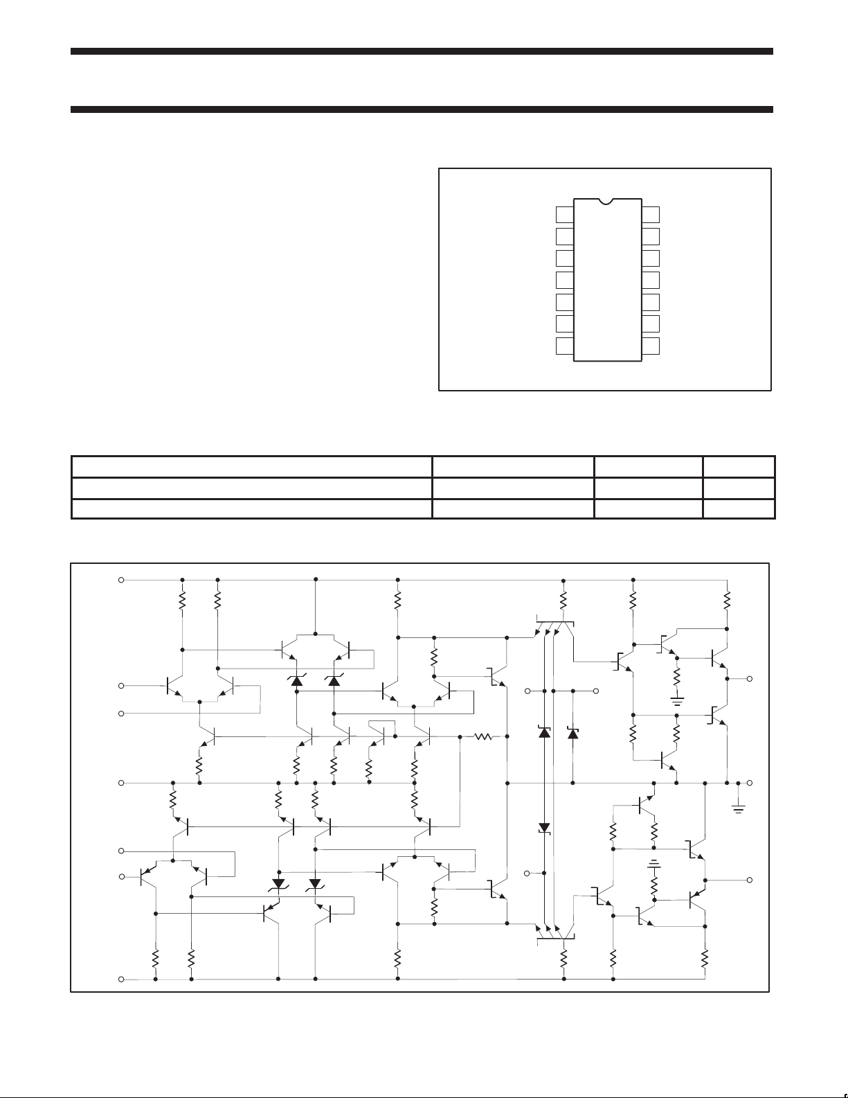
EQUIVALENT SCHEMATIC
V+
14
R2 R1
R17
R20
14
13
12
11
10
9
R21
V+
V–
INPUT 2A
INPUT 2B
NC
OUTPUT 2Y
STROBE 2G
SL00242
R25
Q3
Q4
–
2
+
1
V–
13
+
12
–
11
V+
Q2 Q1
R8
Q16
Q15 Q14
R12 R11
Q9
Q10 Q8
R4
Q18
R5 R3
R10
Q17
D4
Q20
D7
Q21
D6
Q13
R7
D5
Q6
Q11
R15 R6
Q19
Q22 Q23
R16
Q7
Q5
R14
R9
Q24
R18
R19
Q25
R26
6
R28
Q32
R27
5
D2
D3
8
Q31
Q26
R22
Q36
Q32
R29
R30
Q30
Q27
R24
R23
Q29
4
Q28
7
Q35
9
Q34
R34
SL00243
Figure 2. Equivalent Schematic
2001 Aug 03 853-0900 26834
2
Page 3

Philips Semiconductors Product data
NE521High-speed dual-differential comparator/sense amp
BLOCK DIAGRAM
INPUT 1A
INPUT 1B
OUTPUT 1Y
STROBE 1G
STROBE S
(6)
(1)
(2)
(12)
(4)
(5)
INPUT 2A
(11)
INPUT 2B
(9)
OUTPUT 3Y
(8)
STROBE 2G
SL00244
LOGIC FUNCTIONS
V
ID
–
A+, B
VID ≤ –V
OS
–VOS < VID < V
VID ≥ V
OS
X L X H
X X L H
STROBE S STROBE G OUTPUT (Y)
OS
H H L
H H Undefined
H H H
Figure 3. Block Diagram
ABSOLUTE MAXIMUM RATINGS
SYMBOL PARAMETER RATING UNIT
Supply voltage
V+ Positive +7 V
V– Negative -7 V
V
IDR
V
IN
P
D
T
amb
T
stg
T
sld
NOTES:
1. Derate above 25 °C at the following rates:
N package at 11.4 mW/°C
D package at 8.3 mW/°C
Differential input voltage ±6 V
Input voltage
Common mode ±5 V
Strobe/gate +5.25 V
Maximum power dissipation
T
= 25 °C (still-air)
amb
1
N package 1420 mW
D package 1040 mW
Operating temperature range 0 to 70 °C
Storage temperature range –65 to +150 °C
Lead soldering temperature (10 sec. max) +230 °C
2001 Aug 03
3
Page 4

Philips Semiconductors Product data
SYMBOL
PARAMETER
TEST CONDITIONS
UNIT
SYMBOL
PARAMETER
FROM INPUT
TO OUTPUT
UNIT
NE521High-speed dual-differential comparator/sense amp
DC ELECTRICAL CHARACTERISTICS
V+ = +5 V; V– = –5 V, T
V
OS
Input offset voltage V+ = +4.75 V; V– = –4.75 V
At 25 °C 6 7.5 mV
Over temperature range 10 mV
I
BIAS
Input bias current V+ = +5.25 V, V– = –5.25 V
At 25 °C 7.5 20 µA
Over temperature range 40 µA
I
OS
Input offset current V+ = +5.25 V, V– = –5.25 V
At 25 °C 1.0 5 µA
Over temperature range 12 µA
V
CM
Common-mode voltage range V+ = +4.75 V, V– = –4.75 V –3 +3 V
Input current V+ = +5.25 V, V– = –5.25 V
I
IH
High VIH = 2.7 V
Input Current
I
IL
Low VIL = 0.5 V
Output voltage V
V
OH
V
OL
High V+ = +4.75 V; V– = –4.75 V; I
Low V+ = +5.25 V; V– = –5.25 V; I
Supply voltage
V+ Positive 4.75 5.0 5.25 V
V– Negative –4.75 –5.0 –5.25 V
Supply current V+ = 5.25 V; V– = –5.25 V; T
I
CC+
I
CC–
I
SC
Positive 27 35 mA
Negative –15 –28
Short-circuit output current -40 –100 mA
= 0 °C to +70 °C, unless otherwise specified.
amb
LIMITS
Min Typ Max
1G or 2G strobe 50 µA
Common strobe S 100 µA
1G or 2G strobe –2.0 mA
Common strobe S –4.0 mA
= 2.0 V
I(S)
= –1 mA 2.7 3.4 V
LOAD
= 20 mA 0.5 V
LOAD
= 25 °C
amb
AC ELECTRICAL CHARACTERISTICS
T
= 25 °C; RL = 280Ω ; CL=15 pF; V+ = 5 V; V– = 5 V
amb
Large-signal switching speed
Propagation delay
t
PLH(D)
t
PHL(D)
t
PLH(S)
t
PHL(S)
f
MAX
Low to high
High to low
Low to high
High to low
Max. operating frequency 40 55 MHz
NOTES:
1. Response time measured from 0 V point of ±100 mV
2. Response time measured from 1.5 V point of input to 1.5 V point of the output.
2001 Aug 03
1
1
2
2
Amp Output 8 12
Amp Output 6 9 ns
Strobe Output 4.5 10
Strobe Output 3.0 6
10 MHz square wave to the 1.5 V point of the output.
P-P
4
LIMITS
Min Typ Max
Page 5

Philips Semiconductors Product data
NE521High-speed dual-differential comparator/sense amp
TYPICAL PERFORMANCE CHARACTERISTICS
PROPAGATION DELAY (ns)
Response Time for Various
Input Overdrives
10mV
TIME — nS
VS = +5V
T
amb
5mV
= 25oC
100
INPUT VOLTAGE (mV) OUTPUT VOLTAGE (V)
4
3
100mV
2
20mV
1
0
100
50
0
INPUT VOLTAGE (mV) OUTPUT VOLTAGE (V)
0 5 10 15 20 25 30
Propagation Delay for
Various Input Voltages
VS = +5V
TPD (LH)
TPD (HL)
10MHz SQUARE
WAVE INPUT
= 25oC
T
amb
12
10
8
6
20
18
16
14
12
10
PROPAGATION DELAY (ns)
Response Time for Various
Input Overdrives
4
3
50mV
2
1
0
50
0
0 5 10 15 20 25 30
Propagation Delay for
Various Input Voltages
8
6
4
2
TPD (LH)
TPD (HL)
T
amb
V
S
5mV
10mV100mV
TIME — nS
VS = +5V
10MHz SQUARE
WAVE INPUT
T
= 25oC
amb
= 25oC
= +5V
Response Time vs Temperature
12
10
8
6
4
TESPONSE TIME (ns)
2
60 20 –20 +60 +100 +140
TPD (LH)
TPD (HL)
AMBIENT TEMPERATURE (
o
Output Voltage vs
Ambient Temperature
4.0
V
OH
3.0
2.0
OUTPUT VOLTAGE (V)
1.0
V
OL
C)
10 20 30 40 50 60 70
INPUT VOLTAGE (mVp–p)
Input Bias Current vs
12
11
10
µ
9
8
7
INPT BIAS CURRENT ( A)
6
–75 –25 +25 +75 +125
Ambient Temperature
AMBIENT TEMPERATURE
2001 Aug 03
100
1000
INPUT VOLTAGE (m Vp–p)
–25
–75
AMBIENT TEMPERATURE (
+25
+75 +125
o
C)
Input Offset Current vs
1.1
1.0
µ
0.9
0.8
0.7
0.6
INPUT OFSET CURRENT ( A)
0.5
o
(
C)
–75 –25 +25 +75 +125
Ambient Temperature
AMBIENT TEMPERATURES (
o
C)
SL00245
Figure 4. Typical Performance Characteristics
5
Page 6

Philips Semiconductors Product data
NE521High-speed dual-differential comparator/sense amp
DIP14: plastic dual in-line package; 14 leads (300 mil) SOT27-1
2001 Aug 03
6
Page 7

Philips Semiconductors Product data
NE521High-speed dual-differential comparator/sense amp
SO14: plastic small outline package; 14 leads; body width 3.9 mm SOT108-1
2001 Aug 03
7
Page 8

Philips Semiconductors Product data
NE521High-speed dual-differential comparator/sense amp
Data sheet status
Product
Data sheet status
Objective data
Preliminary data
Product data
[1] Please consult the most recently issued data sheet before initiating or completing a design.
[2] The product status of the device(s) described in this data sheet may have changed since this data sheet was published. The latest information is available on the Internet at URL
http://www.semiconductors.philips.com.
[1]
status
Development
Qualification
Production
[2]
Definitions
Short-form specification — The data in a short-form specification is extracted from a full data sheet with the same type number and title. For
detailed information see the relevant data sheet or data handbook.
Limiting values definition — Limiting values given are in accordance with the Absolute Maximum Rating System (IEC 60134). Stress above one
or more of the limiting values may cause permanent damage to the device. These are stress ratings only and operation of the device at these or
at any other conditions above those given in the Characteristics sections of the specification is not implied. Exposure to limiting values for extended
periods may affect device reliability.
Application information — Applications that are described herein for any of these products are for illustrative purposes only. Philips
Semiconductors make no representation or warranty that such applications will be suitable for the specified use without further testing or
modification.
Disclaimers
Life support — These products are not designed for use in life support appliances, devices or systems where malfunction of these products can
reasonably be expected to result in personal injury . Philips Semiconductors customers using or selling these products for use in such applications
do so at their own risk and agree to fully indemnify Philips Semiconductors for any damages resulting from such application.
Right to make changes — Philips Semiconductors reserves the right to make changes, without notice, in the products, including circuits, standard
cells, and/or software, described or contained herein in order to improve design and/or performance. Philips Semiconductors assumes no
responsibility or liability for the use of any of these products, conveys no license or title under any patent, copyright, or mask work right to these
products, and makes no representations or warranties that these products are free from patent, copyright, or mask work right infringement, unless
otherwise specified.
Contact information
For additional information please visit
http://www.semiconductors.philips.com . Fax: +31 40 27 24825
For sales offices addresses send e-mail to:
sales.addresses@www.semiconductors.philips.com.
Definitions
This data sheet contains data from the objective specification for product development.
Philips Semiconductors reserves the right to change the specification in any manner without notice.
This data sheet contains data from the preliminary specification. Supplementary data will be
published at a later date. Philips Semiconductors reserves the right to change the specification
without notice, in order to improve the design and supply the best possible product.
This data sheet contains data from the product specification. Philips Semiconductors reserves the
right to make changes at any time in order to improve the design, manufacturing and supply.
Changes will be communicated according to the Customer Product/Process Change Notification
(CPCN) procedure SNW-SQ-650A.
Koninklijke Philips Electronics N.V. 2001
All rights reserved. Printed in U.S.A.
Date of release: 05-01
Document order number: 9397 750 09192
2001 Aug 03
8
 Loading...