

Page 1
February 1997
NDM3001
3 Phase Brushless Motor Driver
General Description Features
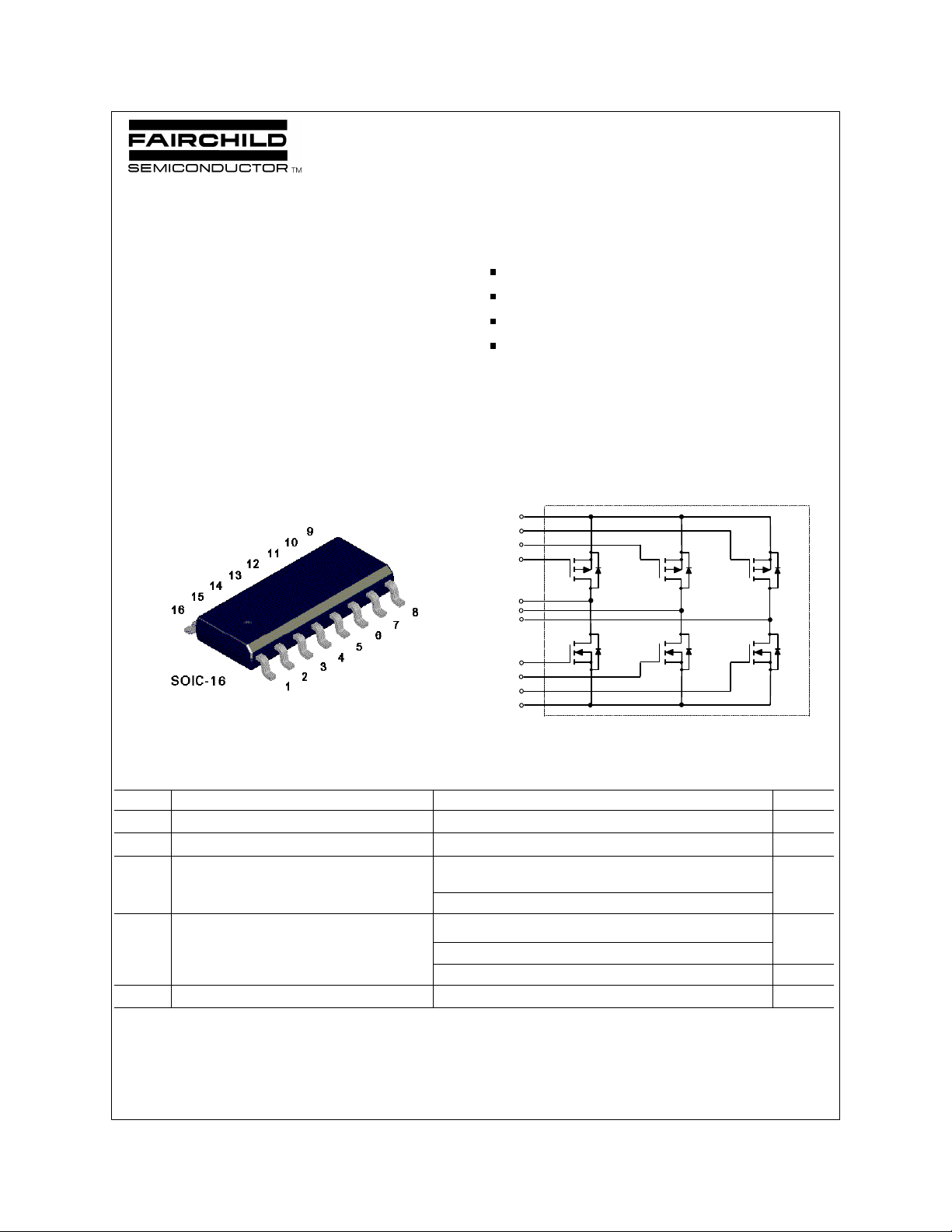
The NDM3001 three phase brushless motor driver consists of
three N-Channel and P-Channel MOSFETs in a half bridge
configuration. These devices are produced using Fairchild's
proprietary, high cell density DMOS technology. This very high
density process is tailored to minimize on-state resistance
which reduces power loss, provide superior switching
performance, and withstand high energy pulses in the
avalanche and commutation modes. These devices are
particularly suited for low voltage 3 phase motor driver such as
disk drive spindle motor control and other half bridge
applications.
________________________________________________________________________________
±2.9 A, ±30 V, 2.5W
High density cell design for extremely low R
DS(ON)
High power and current handling capability.
Industry standard SOIC-16 surface mount package.
11,14
10
12
15
Q1
.
Q5Q3
1,16
4,13
8,9
Absolute Maximum Ratings T
= 25°C unless otherwise noted
A
2
5
7
3,6
Q2
Q6Q4
Symbol Parameter NDM3001 Units
V
DSS
V
GSS
I
D
Drain-Source Voltage (All Types) ±30 V
Gate-Source Voltage (All Types) ±20 V
Drain Current Q1+Q4 or Q1+Q6 or Q3+Q2 -
±2.9 A
Continuous Q3+Q6 or Q5+Q2 or Q5+Q4
- Pulsed (Note 1a & 2) ±10
P
TJ,T
D
Total Power Dissipation (Note 1a)
Q1+Q4 or Q1+Q6 or Q3+Q2 or (Note 1b)
Q3+Q6 or Q5+Q2 or Q5+Q4
(Note 1c)
Operating and Storage Temperature Range -55 to 150 °C
STG
2.5 W
1.6
1.4
© 1997 Fairchild Semiconductor Corporation
NDM3001 Rev.C
Page 2
THERMAL CHARACTERISTICS
R
θ
Thermal Resistance, Junction-to-Ambient
JA
Q1+Q4 or Q1+Q6 or Q3+Q2 or
Q3+Q6 or Q5+Q2 or Q5+Q4 (Note 1a)
R
θ
Thermal Resistance, Junction-to-Case
JC
Q1+Q4 or Q1+Q6 or Q3+Q2 or
Q3+Q6 or Q5+Q2 or Q5+Q4 (Note 1)
50 °C/W
20 °C/W
Electrical Characteristics (T
= 25°C unless otherwise noted)
A
Symbol Parameter Conditions Type Min Typ Max Units
OFF CHARACTERISTICS
BV
I
DSS
I
GSS
DSS
Drain-Source Breakdown Voltage
Zero Gate Voltage Drain Current VDS = ±24 V, V
VGS = 0 V, ID = ± 250 µA
= 0 V All ±1 µA
GS
TJ=55oC
Gate - Body Leakage, Forward VGS = ±20 V, VDS = 0 V All ±100 nA
All ±30 V
±10 µA
ON CHARACTERISTICS (Note 3)
V
R
GS(th)
DS(ON)
Gate Threshold Voltage
Static Drain-Source
On-Resistance
VDS = VGS, ID = -250 µA
TJ=125oC
VDS = VGS, ID = 250 µA
TJ=125oC
VGS = -10 V, ID = -2.9 A
TJ=125oC
Q1, Q3, Q5 - 1 -1.6 -2 V
- 0.75 -1.3 -1.5
Q2, Q4, Q6 1 1.5 2
0.75 1.2 1.5
Q1, Q3, Q5 0.19 0.24
0.27 0.45
Ω
VGS = -4.5 V, ID = -2.2 A 0.3 0.36
VGS = 10 V, ID = 2.9 A
Q2, Q4, Q6 0.09 0.115
TJ=125oC 0.126 0.221
0.13 0.16
I
D(on)
VGS = 4.5 V, ID = 2.2 A
On-State Drain Current VGS = 10 V, VDS = -5 V Q1, Q3, Q5 -10 A
VGS = 10 V, VDS = 5 V
Q2, Q4, Q6 10
DYNAMIC CHARACTERISTICS
C
iss
C
oss
Input Capacitance Q1, Q3, Q5
VDS = -15 V, V
f = 1.0 MHz
GS
= 0 V,
Output Capacitance Q1, Q3, Q5 140 pF
Q2, Q4, Q6 VDS =
C
rss
Reverse Transfer Capacitance Q1, Q3, Q5 50 pF
15 V, V
f = 1.0 MHz
GS
= 0 V,
Q1, Q3, Q5 260 pF
Q2, Q4, Q6 185
Q2, Q4, Q6 115
Q2, Q4, Q6 40
NDM3001 Rev.C
Page 3
Electrical Characteristics (T
= 25°C unless otherwise noted)
A
Symbol Parameter Conditions Type Min Typ Max Units
SWITCHING CHARACTERISTICS
t
t
t
t
D(on)
r
D(off)
f
Turn - On Delay Time Q1, Q3, Q5
Turn - On Rise Time Q1, Q3, Q5 13 40 ns
Turn - Off Delay Time Q1, Q3, Q5 21 90 ns
Turn - Off Fall Time Q1, Q3, Q5 5 50 ns
(Note 3)
V
= -15 V, ID = -1 A,
DD
V
= -10 V, R
GEN
Q2, Q4, Q6
V
= 15 V, ID = 1 A,
DD
V
= 10 V, R
GEN
GEN
GEN
= 6 Ω
= 6 Ω
Q1, Q3, Q5 10 40 ns
Q2, Q4, Q6 9 40
Q2, Q4, Q6 21 40
Q2, Q4, Q6 21 90
Q2, Q4, Q6 8 50
Q
g
Q
gs
Total Gate Charge Q1, Q3, Q5
V
= -10 V,
DS
I
= -3.0 A, VGS = -10 V
Gate-Source Charge Q1, Q3, Q5 1.6 nC
D
Q2, Q4, Q6
V
= 10 V,
Q
gd
Gate-Drain Charge Q1, Q3, Q5 3 nC
DS
I
= 3.0 A, VGS = 10 V
D
Q1, Q3, Q5 10 25 nC
Q2, Q4, Q6 9.5 25
Q2, Q4, Q6 1.5
Q2, Q4, Q6 2.5
DRAIN-SOURCE DIODE CHARACTERISTICS AND MAXIMUM RATINGS
I
S
Maximum Continuous Drain-Source Diode Forward Current Q1, Q3, Q5 -1.2 A
Q2, Q4, Q6 1.2
V
SD
t
rr
Notes:
1. R
design while R
P
Typical R
Drain-Source Diode Forward
Voltage
Reverse Recovery Time
is the sum of the junction-to-case and case-to-ambient thermal resistance where the case thermal reference is defined as the solder mounting surface of the drain pins. R
JA
θ
(t)
D
is determined by the user's board design.
CA
θ
=
JA
θ
a. 50
b. 80
c. 90
T
R
T
J−TA
=
(t)
R
JA
θ
θ
JC
using the board layouts shown below on 4.5"x5" FR-4 PCB in a still air environment:
o
C/W when mounted on a 1 in2 pad of 2oz cpper.
o
C/W when mounted on a 0.027 in2 pad of 2oz cpper.
o
C/W when mounted on a 0.0028 in2 pad of 2oz cpper.
J−TA
+R
2
=I
(t)×R
DS(ON) T
D
(t)
θ
CA
V
= 0 V, IS = -3.0 A
GS
= 0 V, IS = 3.0 A
V
GS
V
= 0 V, I F = ±3.0 A,
GS
dI
/dt = 100 A/µs
F
J
(Note 3)
(Note 3)
1a 1b
Q1, Q3, Q5 -0.8 -1.3 V
Q2, Q4, Q6 0.8 1.3
All 100 ns
is guaranteed by
JC
θ
1c
2. Pulse Test: Pulse Width <
Scale 1 : 1 on letter size paper
300µs, Duty Cycle < 2.0%.
NDM3001 Rev. C
Page 4
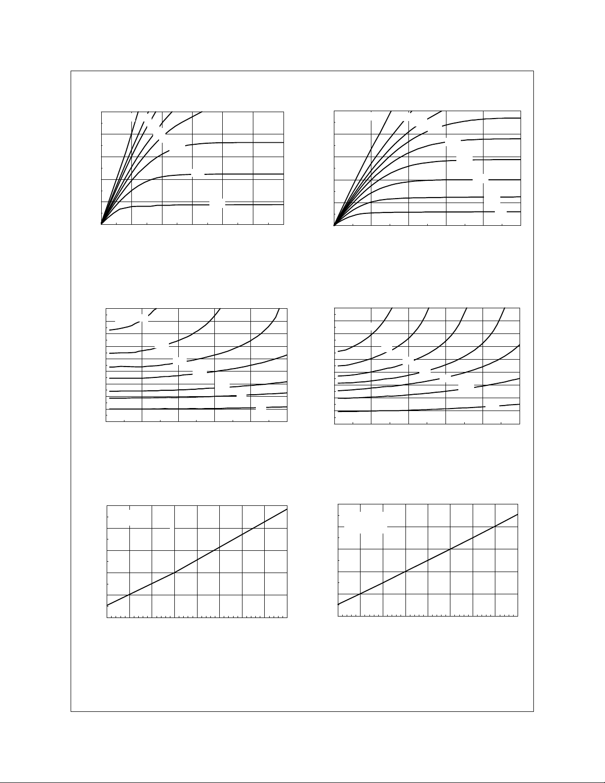
Typical Electrical Characteristics
10
V =10V
GS
8
6
4
2
D
I , DRAIN-SOURCE CURRENT (A)
0
0 0.5 1 1.5 2 2.5 3
Figure 1. N-Channel On-Region Characteristic.
2.6
2.4
2.2
2
1.8
1.6
1.4
DS(on)
R , NORMALIZED
1.2
DRAIN-SOURCE ON-RESISTANCE
1
0.8
0 2 4 6 8 10
V = 3.5V
GS
7.0
6.0
5.0
4.5
4.0
3.5
3.0
V , DRAIN-SOURCE VOLTAGE (V)
DS
4.0
4.5
5.0
6.0
I , DRAIN CURRENT (A)
D
-10
V = -10V
GS
-8
-6
-4
-2
D
I , DRAIN-SOURCE CURRENT (A)
0
-7.0
-6.0
-5.5
-5.0
-4.5
V , DRAIN-SOURCE VOLTAGE (V)
DS
-4.0
-3.5
-3.0
-5-4-3-2-10
Figure 2. P-Channel On-Region
Characteristics.
2.6
2.4
V = -4.0V
GS
2.2
2
1.8
1.6
1.4
7
10
DS(on)
R , NORMALIZED
1.2
DRAIN-SOURCE ON-RESISTANCE
1
0.8
-4.5
-5.0
-5.5
I , DRAIN CURRENT (A)
D
-6.0
-7.0
-10
-10-8-6-4-20
Figure 3. N-Channel On-Resistance Variation with
Gate Voltage and Drain Current.
1.6
ID= 2.9A
VGS= 10V
1.4
1.2
1
DS(ON)
R , NORMALIZED
0.8
DRAIN-SOURCE ON-RESISTANCE
0.6
-50 -25 0 25 50 75 100 125 150
T , JUNCTION TEMPERATURE (°C)
J
Figure 5. N-Channel On-Resistance Variation
with Temperature.
NDM3001 Rev.C
Figure 4. P-Channel On-Resistance Variation
with Gate Voltage and Drain Current.
1.6
I = -2.9A
D
V = -10V
1.4
GS
1.2
1
DS(ON)
R , NORMALIZED
0.8
DRAIN-SOURCE ON-RESISTANCE
0.6
-50 -25 0 25 50 75 100 125 150
T , JUNCTION TEMPERATURE (°C)
J
Figure 6. P-Channel On-Resistance Variation
with Temperature.
Page 5

Typical Electrical Characteristics
2
V = 10 V
GS
1.8
1.6
1.4
1.2
1
DS(on)
0.8
R , NORMALIZED
0.6
DRAIN-SOURCE ON-RESISTANCE
0.4
0 1 2 3 4 5
T = 125°C
J
25°C
-55°C
I , DRAIN CURRENT (A)
D
Figure 7. N-Channel On-Resistance Variation
with Drain Current and Temperature.
5
V =10V
DS
4
3
2
D
I , DRAIN CURRENT (A)
1
0
1 1.5 2 2.5 3 3.5 4
T = -55°C
J
25°C
125°C
V , GATE TO SOURCE VOLTAGE (V)
GS
1.8
V = -10V
GS
1.6
T = 125°C
J
1.4
1.2
1
DS(on)
R , NORMALIZED
0.8
DRAIN-SOURCE ON-RESISTANCE
25°C
-55°C
0.6
I , DRAIN CURRENT (A)
D
Figure 8. P-Channel On-Resistance Variation with
Drain Current and Temperature.
-5
V = -10V
DS
-4
-3
-2
D
I , DRAIN CURRENT (A)
-1
0
T = -55°C
J
V , GATE TO SOURCE VOLTAGE (V)
GS
25°C
125°C
-5-4-3-2-10
-5-4-3-2-1
Figure 9. N-Channel Transfer
Characteristics.
1.2
V = V
1.1
1
0.9
th
V , NORMALIZED
0.8
0.7
GATE-SOURCE THRESHOLD VOLTAGE
0.6
-50 -25 0 25 50 75 100 125 150
T , JUNCTION TEMPERATURE (°C)
J
DS GS
I = 250µA
D
Figure 11. N-Channel Gate Threshold Variation with
Temperature.
NDM3001 Rev.C
Figure 10. P-Channel Transfer
Characteristics.
1.2
V = V
DS
I =- 250µA
1.1
1
0.9
GS(th)
V , NORMALIZED
0.8
GATE-SOURCE THRESHOLD VOLTAGE
0.7
-50 -25 0 25 50 75 100 125 150
T , JUNCTION TEMPERATURE (°C)
J
D
Figure 12. P-Channel Gate Threshold Variation
with Temperature.
GS
Page 6

Typical Electrical Characteristics
1.12
I = 250µA
D
1.08
1.04
1
DSS
BV , NORMALIZED
0.96
DRAIN-SOURCE BREAKDOWN VOLTAGE
0.92
-50 -25 0 25 50 75 100 125 150
T , JUNCTION TEMPERATURE (°C)
J
Figure 13. N-Channel Breakdown Voltage
Variation with Temperature.
500
300
200
100
60
CAPACITANCE (pF)
f = 1 MHz
40
V = 0V
GS
20
0.1 0.2 0.5 1 2 5 10 20 30
V , DRAIN TO SOURCE VOLTAGE (V)
DS
C
C
C
iss
oss
rss
1.08
I = -250µA
1.06
1.04
1.02
DSS
0.98
BV , NORMALIZED
0.96
DRAIN-SOURCE BREAKDOWN VOLTAGE
0.94
D
1
-50 -25 0 25 50 75 100 125 150
T , JUNCTION TEMPERATURE (°C)
J
Figure 14. P-Channel Breakdown Voltage
Variation with Temperature.
600
400
300
200
100
CAPACITANCE (pF)
f = 1 MHz
50
V = 0 V
GS
30
0.1 0.2 0.5 1 2 5 10 20 30
-V , DRAIN TO SOURCE VOLTAGE (V)
DS
C
C
C
iss
oss
rss
Figure 15. N-Channel Capacitance
Characteristics.
10
I = 2.9A
D
8
6
4
2
GS
V , GATE-SOURCE VOLTAGE (V)
0
0 2 4 6 8
Q , GATE CHARGE (nC)
g
V = 5V
DS
10V
15V
Figure 17. N-Channel Gate Charge Characteristics.
NDM3001 Rev.C
Figure 16. P-Channel Capacitance
Characteristics.
10
I = -2.9A
D
8
6
4
2
GS
-V , GATE-SOURCE VOLTAGE (V)
0
0 1 2 3 4 5 6 7
Q , GATE CHARGE (nC)
g
V = -5V
DS
-15V
Figure 18. P-Channel Gate Charge
Characteristics.
-10V
Page 7

Typical Electrical Characteristics
5
V = 0V
GS
1
0.1
0.01
0.001
S
I , REVERSE DRAIN CURRENT (A)
0.0001
0 0.2 0.4 0.6 0.8 1 1.2
V , BODY DIODE FORWARD VOLTAGE (V)
SD
T = 125°C
J
25°C
-55°C
Figure19. N-Channel Body Diode Forward Voltage
Variation with Source Current and
Temperature.
7
V = 10V
DS
6
5
4
3
2
1
FS
g , TRANSCONDUCTANCE (SIEMENS)
0
0 2 4 6 8 10
I , DRAIN CURRENT (A)
D
T = -55°C
J
25°C
125°C
5
V = 0V
GS
2
1
0.5
0.1
0.01
0.001
S
-I , REVERSE DRAIN CURRENT (A)
0.0001
0 0.2 0.4 0.6 0.8 1 1.2
-V , BODY DIODE FORWARD VOLTAGE (V)
SD
T = 125°C
J
25°C
-55°C
Figure 20. P-Channel Body Diode Forward Voltage
Variation with Source Current and
Temperature.
5
V =-10V
DS
T = -55°C
4
3
2
1
FS
g , TRANSCONDUCTANCE (SIEMENS)
0
I , DRAIN CURRENT (A)
D
J
25°C
125°C
-5-4-3-2-10
Figure 21. N-Channel Transconductance Variation
with Drain Current and Temperature.
V
DD
V
IN
R
L
D
V
GS
R
GEN
G
DUT
S
Figure 23. N or P-Channel Switching Test Circuit.
NDM3001 Rev.C
V
OUT
Figure 22. P-Channel Transconductance Variation
with Drain Current and Temperature.
t t
on off
t
d(off)
90%
10%
t
f
V
t
d(on)
OUT
10%
t
r
90%
90%
V
IN
50%
50%
10%
PULSE WIDTH
Figure 24. N or P-Channel Switching Waveforms.
Page 8

Typical Thermal and Electrical Characteristics
3.5
3
2.5
2
1b
1.5
1c
DC POWER DISSIPATION (W)
1
0.5
0 0.2 0.4 0.6 0.8 1
2oz COPPER MOUNTING PAD AREA (in )
4.5"x5" FR-4 PCB
Ta = 25C
Still Air
2
Figure 25. SOIC-16 3 Leadframe Device DC Power
Dissipation versus Copper Mounting Pad Area.
4.5
4
1b
3.5
1c
3
D
I , DC DRAIN CURRENT (A)
2.5
0 0.2 0.4 0.6 0.8 1
2oz COPPER MOUNTING PAD AREA (in )
4.5"x5" FR-4 PCB
Ta = 25C
Still Air
Vgs =10V
2
3.5
1a
3
2.5
1b
1c
2
D
I , DC DRAIN CURRENT (A)
1.5
0 0.2 0.4 0.6 0.8 1
2oz COPPER MOUNTING PAD AREA (in )
4.5"x5" FR-4 PCB
Ta = 25C
Still Air
Vgs = -10V
2
1a
Figure 26. P-Ch DC Drain Current Capability versus
Copper Mounting Pad Area.
20
10
1a
3
RDS(ON) LIMIT
1
0.3
V = ±10V
0.1
D
±I , DRAIN CURRENT (A)
0.03
0.01
0.5 0.8 1 2 5 10 30 50
GS
SINGLE PULSE
R = See Note 1c
JA
θ
T = 25°C
A
±V , DRAIN-SOURCE VOLTAGE (V)
DS
10s
DC
1ms
10ms
100ms
1s
Figure 27. N-Ch DC Drain Current Capability
versus Copper Mounting Pad Area.
1
0.5
0.2
0.1
0.05
0.02
0.01
0.005
r(t), NORMALIZED EFFECTIVE
0.002
TRANSIENT THERMAL RESISTANCE
0.001
0.0001 0.001 0.01 0.1 1 10 100 300
D = 0.5
0.2
0.1
0.05
0.02
0.01
Single Pulse
Figure 29. Transient Thermal Response Curve.
Note: Thermal characterization performed using the conditions described in note 1c. Transient thermal response will change
depending on the circuit board design.
NDM3001 Rev.C
t , TIME (sec)
1
Figure 28. P-Ch Typical Safe Operating Area.
R (t) = r(t) * R
JA
θ
R = See Note 1c
JA
θ
P(pk)
t
1
t
2
T - T = P * R (t)
J
A
Duty Cycle, D = t / t
JA
θ
JA
θ
2
1
Page 9

g
g
g
ging
g
g
g
y
y
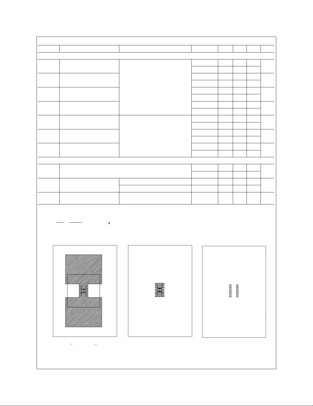
SOIC-16 Tape and Reel Data and Package Dimensions
SOIC(16lds) Packaging
Configuration:
Fi
ure 1.0
Customized
Label
SOIC (16lds) Packaging Information
Packaging Option
Packaging type
Qty per Reel/Tube/Bag
Reel Size
Box Dimension (mm)
Max qty per Box
Weight per unit (gm)
Weight per Reel (kg)
Note/Comments
Standard
(no flow code)
2,500 45
13" Dia
343x64x343 530x130x83
5,000 13,500
0.1437 0.1437
0.7735 -
TNR
L86Z
Rail/Tube
-
ELECTROSTATIC
SENSITIVE DEVICES
DO NOT SHIP OR STORE NEAR STRONG ELECTROSTATIC
ELECTROMAGNETIC, MAGNETIC OR RADIOACTIVE FIELDS
TNR DATE
PT NUMBER
PEEL STRENGTH MIN ______________gms
MAX _____________ gms
ESD Label
Embossed Carrier Tape
Antistatic Cover Tape
Static Dissipative
F63TNR
Label
Packaging Description:
SOIC-16 parts are shipped in tape. The carrier tape is
made from a dissipative (carbon filled) polycarbonate
resin. The cover tape is a multilayer film (Heat Activated
Adhesive in nature) primarily composed of polyester film,
adhesi ve layer, sea lant, and anti-static sprayed a
These reeled parts in standard option are shipped with
2,500 uni t s pe r 13" o r 33 0c m d ia met er reel . Th e reel s ar e
dark blue in color and is made of polystyrene plastic (antistatic coated). This and some other options are further
described in the Packa
These full reels are individually barcode labeled and
placed inside a standard intermediate box (illustrated in
fi
ure 1.0) made of recyclable corrugated bro wn paper.
One box contains two reels maximum. And these boxes
are placed inside a barcode labeled shippin
comes in different sizes dependin
shippe d.
NDM3001
F
NDM3001
D85AB
NDM3001
F
D85AB
F
D85AB
SOIC-16 Unit Orientat ion
343mm x 342mm x 64mm
Stand a r d In termedia t e bo x
Information table.
on the number of pa rts
NDM3001
F
D85AB
box which
ent.
D85AB
F
NDM3001
Pin 1
F63TNR Label sample
LOT: CBVK741B019
FSID: NDM3000
D/C1: D9842 QTY1: SPEC REV:
D/C2: QTY2: CPN:
QTY: 2500
SPEC:
N/F: F (F63TNR)3
SOIC(16lds) Tape Leader and Trailer
Configuration:
Carrier Tape
Cover Tape
ure 2.0
Fi
Trailer Tape
640mm minimum or
80 empt
pockets
F63TNR Label
ESD Label
Components
ESD Label
Leader Tape
1680mm minimum or
210 empt
pockets
October 1999, Rev. B
F63TNR Label
Page 10

SOIC-16 Tape and Reel Data and Package Dimensions, continued
g
g
(
)
SOIC(16lds) Embossed Carrier Tape
Configuration:
T
K0
Wc
Tc
Fi
B0
ure 3.0
P0
A0
User Direction of Feed
Dimensions are in millimeter
D0
F
P1
D1
E1
W
E2
Pkg type
SOIC
16lds
(16mm)
Notes: A0, B0, and K0 dimensions are determined with respect to the EIA/Jedec RS-481
rotational and lateral movement requirements (see sketches A, B, and C).
SOIC(16lds) Reel Configuration:
A0 B0 W D0 D1 E1 E2 F P1 P0 K0 T Wc Tc
6.60
10.35
16.0
1.55
1.60
1.75
14.25
+/-0.30
+/-0.25
10 deg maximum component rotation
Sketch A (Side or Front Sectional View)
Component Rotation
+/-0.3
+/-0.05
Fi
+/-0.10
ure 4.0
+/-0.10
B0
7.50
min
+/-0.05
10 deg maximum
A0
Sketch B (Top View)
Component Rotation
W1 Measured at Hub
Dim A
max
Dim N
8.0
+/-0.1
Typical
component
cavity
center line
Typical
component
center line
Dim A
Max
Dim D
min
4.0
+/-0.1
2.40
0.450
+/-0.40
+/-0.150
0.9mm
maximum
Sketch C (Top View)
Component lateral movement
B Min
Dim C
DETAIL AA
13.0
+/-0.3
0.9mm
maximum
0.06
+/-0.02
W3
13" Diameter Option
See detail AA
W2 max Measured at Hub
Dimensions are in inches and millimeters
Tape Size
16mm 13" Dia
Reel
Option
Dim A Dim B Dim C Dim D Dim N Dim W1 Dim W2 Dim W3 (LSL-USL)
13.00
0.059
1.5
512 +0.020/- 0.008
13 +0.5/-0.2
330
0.795
20.2
4.00
100
0.646 +0.078/-0.000
16.4 +2/0
0.882
22.4
0.626 – 0.764
15.9 – 19.4
July 1999, Rev. B
Page 11

SOIC-16 Tape and Reel Data and Package Dimensions, continued
SOIC-16 (FS PKG Code S3)
1:1
Scale 1:1 on letter size paper
Dimensions shown below are in:
inches [millimeters]
Part Weight per unit (gram): 0.1437
October 1999, Rev. A1
Page 12

TRADEMARKS
The following are registered and unregistered trademarks Fairchild Semiconductor owns or is authorized to use and is
not intended to be an exhaustive list of all such trademarks.
ACEx™
CoolFET™
CROSSVOLT™
2
E
CMOS
TM
FACT™
FACT Quiet Series™
®
FAST
FASTr™
GTO™
HiSeC™
ISOPLANAR™
MICROWIRE™
POP™
PowerTrench™
QFET™
QS™
Quiet Series™
SuperSOT™-3
SuperSOT™-6
SuperSOT™-8
TinyLogic™
UHC™
VCX™
DISCLAIMER
FAIRCHILD SEMICONDUCTOR RESERVES THE RIGHT TO MAKE CHANGES WITHOUT FURTHER
NOTICE TO ANY PRODUCTS HEREIN TO IMPROVE RELIABILITY, FUNCTION OR DESIGN. FAIRCHILD
DOES NOT ASSUME ANY LIABILITY ARISING OUT OF THE APPLICA TION OR USE OF ANY PRODUCT
OR CIRCUIT DESCRIBED HEREIN; NEITHER DOES IT CONVEY ANY LICENSE UNDER ITS PATENT
RIGHTS, NOR THE RIGHTS OF OTHERS.
LIFE SUPPORT POLICY
FAIRCHILD’S PRODUCTS ARE NOT AUTHORIZED FOR USE AS CRITICAL COMPONENTS IN LIFE SUPPORT
DEVICES OR SYSTEMS WITHOUT THE EXPRESS WRITTEN APPROV AL OF FAIRCHILD SEMICONDUCTOR CORPORA TION.
As used herein:
1. Life support devices or systems are devices or
systems which, (a) are intended for surgical implant into
the body, or (b) support or sustain life, or (c) whose
failure to perform when properly used in accordance
with instructions for use provided in the labeling, can be
reasonably expected to result in significant injury to the
user.
2. A critical component is any component of a life
support device or system whose failure to perform can
be reasonably expected to cause the failure of the life
support device or system, or to affect its safety or
effectiveness.
PRODUCT STA TUS DEFINITIONS
Definition of Terms
Datasheet Identification Product Status Definition
Advance Information
Preliminary
No Identification Needed
Obsolete
Formative or
In Design
First Production
Full Production
Not In Production
This datasheet contains the design specifications for
product development. Specifications may change in
any manner without notice.
This datasheet contains preliminary data, and
supplementary data will be published at a later date.
Fairchild Semiconductor reserves the right to make
changes at any time without notice in order to improve
design.
This datasheet contains final specifications. Fairchild
Semiconductor reserves the right to make changes at
any time without notice in order to improve design.
This datasheet contains specifications on a product
that has been discontinued by Fairchild semiconductor.
The datasheet is printed for reference information only.
 Loading...