

Page 1
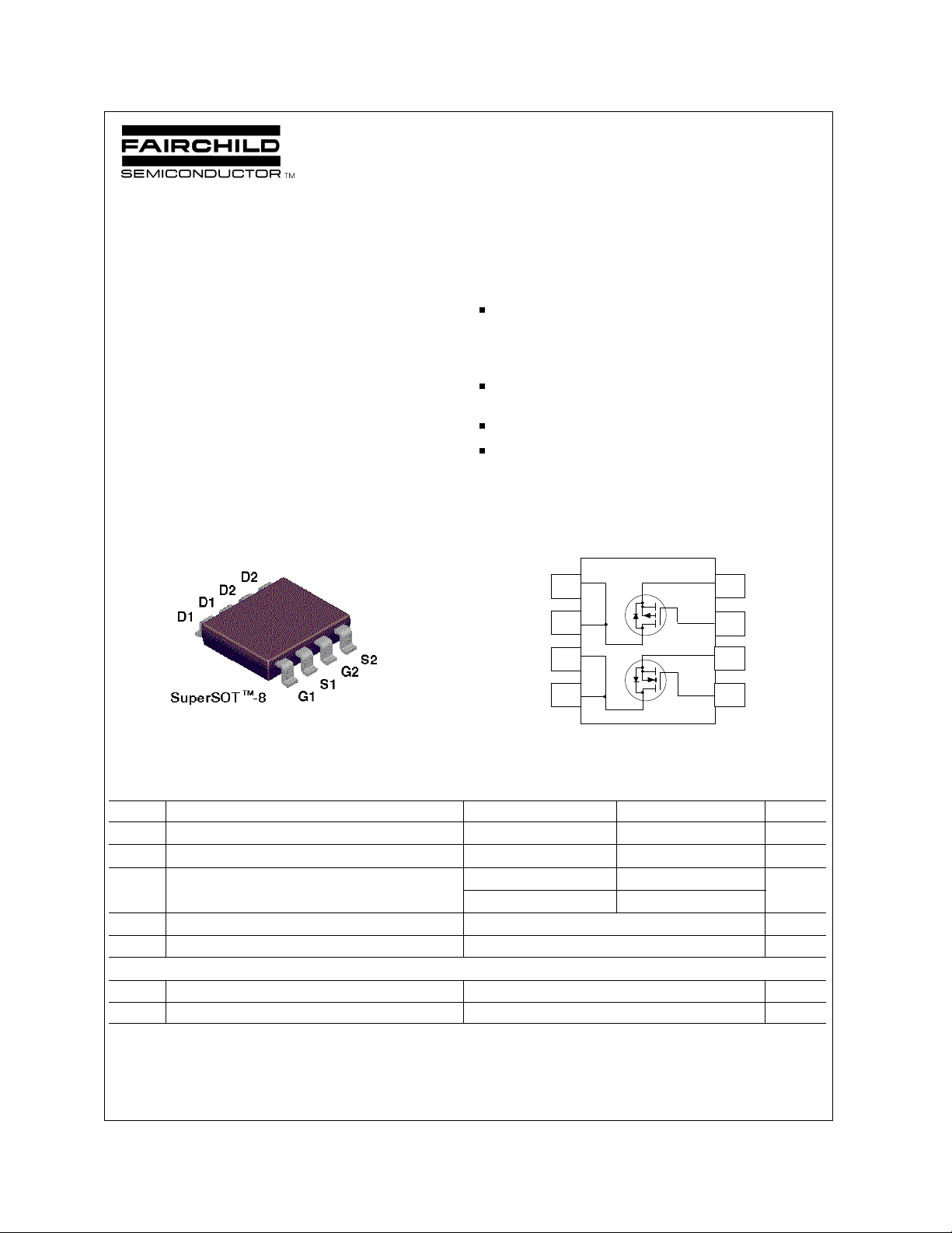
NDH8521C
Dual N & P-Channel Enhancement Mode Field Effect Transistor
General Description Features
May 1997
These dual N- and P-Channel enhancement mode power field
effect transistors are produced using Fairchild's proprietary,
high cell density, DMOS technology. This very high density
process is especially tailored to minimize on-state resistance
and provide superior switching performance. These devices
are particularly suited for low voltage applications such as
notebook computer power management and other battery
powered circuits where fast switching, low in-line power loss,
and resistance to transients are needed.
N-Ch 3.8 A, 30 V, R
R
P-Ch -2.7 A, -30 V,R
R
=0.033Ω @ VGS=10 V
DS(ON)
=0.05 Ω @ VGS=4.5 V
DS(ON)
=0.07 Ω @ VGS=-10 V
DS(ON)
=0.115 Ω @ VGS=-4.5 V.
DS(ON)
Proprietary SuperSOTTM-8 package design using copper lead
frame for superior thermal and electrical capabilities.
High density cell design for extremely low R
DS(ON)
.
Exceptional on-resistance and maximum DC current
capability.
________________________________________________________________________________
5
6
7
8
4
3
2
1
Absolute Maximum Ratings T
= 25°C unless otherwise noted
A
Symbol Parameter N-Channel P-Channel Units
V
DSS
V
GSS
I
D
Drain-Source Voltage 30 -30 V
Gate-Source Voltage ±20 ±20 V
Drain Current - Continuous (Note 1) 3.8 -2.7 A
- Pulsed 10.5 -8
P
D
TJ,T
Power Dissipation for Single Operation (Note 1) 0.8 W
Operating and Storage Temperature Range -55 to 150 °C
STG
THERMAL CHARACTERISTICS
R
θJA
R
θJC
© 1997 Fairchild Semiconductor Corporation
Thermal Resistance, Junction-to-Ambient (Note 1) 156 °C/W
Thermal Resistance, Junction-to-Case (Note 1) 40 °C/W
NDH8521C Rev.C
Page 2
Electrical Characteristics (T
= 25°C unless otherwise noted)
A
Symbol Parameter Conditions Type Min Typ Max Units
OFF CHARACTERISTICS
BV
I
DSS
I
GSSF
I
GSSR
DSS
Drain-Source Breakdown Voltage VGS = 0 V, ID = 250 µA N-Ch 30 V
VGS = 0 V, ID = -250 µA
Zero Gate Voltage Drain Current VDS = 24 V, V
VDS = -24 V, V
= 0 V N-Ch 1 µA
GS
TJ = 55oC
= 0 V P-Ch -1 µA
GS
TJ = 55oC
P-Ch -30 V
10 µA
-10 µA
Gate - Body Leakage, Forward VGS = 20 V, VDS = 0 V All 100 nA
Gate - Body Leakage, Reverse
VGS = -20 V, VDS= 0 V
All -100 nA
ON CHARACTERISTICS (Note 2)
V
R
GS(th)
DS(ON)
Gate Threshold Voltage
Static Drain-Source On-Resistance
VDS = VGS, ID = 250 µA
TJ = 125oC
VDS = VGS, ID = -250 µA
TJ = 125oC
VGS = 10 V, ID = 3.8 A
N-Ch 1 1.67 2 V
0.8 1.04 1.6
P-Ch -1 -1.6 -2
-0.8 -1.2 -1.6
N-Ch 0.027 0.033
Ω
TJ = 125oC 0.04 0.063
VGS = 4.5 V, ID = 3.2 A
0.041 0.05
VGS = -10 V, ID = -2.7 A P-Ch 0.062 0.07
TJ = 125oC
0.088 0.125
VGS = -4.5 V, ID = - 2.1 A 0.102 0.115
I
D(on)
On-State Drain Current
VGS = 10 V, VDS = 5 V
N-Ch 10.5 A
VGS = 4.5 V, VDS = 5 V 9
VGS = -10 V, VDS = -5 V
P-Ch -8
VGS = -4.5 V, VDS = -5 V -3
g
FS
Forward Transconductance
VDS = 5 V, ID = 3.8 A
N-Ch 9 S
VDS = -5 V, ID = -2.7 A P-Ch 5.5
DYNAMIC CHARACTERISTICS
C
iss
Input Capacitance N-Channel
VDS = 15 V, VGS = 0 V,
f = 1.0 MHz
C
oss
C
rss
Output Capacitance N-Ch 310 pF
P-Channel
Reverse Transfer Capacitance N-Ch 125 pF
VDS = -15 V, VGS = 0 V,
f = 1.0 MHz
N-Ch 500 pF
P-Ch 560
P-Ch 340
P-Ch 130
NDH8521C Rev.C
Page 3
Electrical Characteristics (T
= 25°C unless otherwise noted)
A
Symbol Parameter Conditions Type Min Typ Max Units
SWITCHING CHARACTERISTICS (Note 2)
t
t
t
t
D(on)
r
D(off)
f
Turn - On Delay Time N-Channel
VDD = 10 V, ID = 1 A,
V
= 10 V, R
Turn - On Rise Time N-Ch 15 28 ns
GEN
GEN
= 6 Ω
P-Channel
Turn - Off Delay Time N-Ch 20 35 ns
VDD = -10 V, ID = -1 A,
V
= -10 V, R
GEN
GEN
= 6 Ω
N-Ch 10 18 ns
P-Ch 13 25
P-Ch 16 30
P-Ch 35 70
Turn - Off Fall Time N-Ch 9 18 ns
P-Ch 40 80
Q
g
Q
gs
Q
gd
Total Gate Charge N-Channel
VDS = 15 V,
ID = 3.8 A, VGS = 10 V
N-Ch 18 25 nC
P-Ch 19 27
Gate-Source Charge N-Ch 1.8 nC
P-Channel
Gate-Drain Charge N-Ch 4.2 nC
VDS = -15 V,
ID = -2.7 A, VGS = -10 V
P-Ch 3.8
P-Ch 4.7
DRAIN-SOURCE DIODE CHARACTERISTICS AND MAXIMUM RATINGS
I
S
Maximum Continuous Drain-Source Diode Forward Current N-Ch 0.67 A
P-Ch -0.67
V
Notes:
1. R
SD
design while R
Drain-Source Diode Forward Voltage
is the sum of the junction-to-case and case-to-ambient thermal resistance where the case thermal reference is defined as the solder mounting surface of the drain pins. R
JA
θ
is determined by the user's board design.
CA
θ
VGS = 0 V, IS = 0.67 A
VGS = 0 V, IS = -0.67 A
(Note2)
(Note2)
N-Ch 0.72 1.2 V
P-Ch -0.74 -1.2
is guaranteed by
JC
θ
T
(t)
P
=
D
R
Scale 1 : 1 on letter size paper.
2. Pulse Test: Pulse Width < 300µs, Duty Cycle < 2.0%.
J−TA
θJA
T
J−TA
=
(t)
R
θJC+RθCA
2
= I
(t)×R
D
(t)
DS(O N ) T
Typical R
for single device operation using the board layout shown below on 4.5"x5" FR-4 PCB in a still air environment:
JA
J
θ
156oC/W when mounted on a 0.0025 in2 pad of 2oz copper.
NDH8521C Rev.C
Page 4

Typical Electrical Characteristics: N-Channel
20
V =10V
GS
16
12
8
4
D
I , DRAIN-SOURCE CURRENT (A)
0
0 0.5 1 1.5 2 2.5 3
6.0
5.0
4.5
4.0
3.5
V , DRAIN-SOURCE VOLTAGE (V)
DS
Figure 1. N-Channel On-Region Characteristics.
1.8
I = 3.8A
D
V = 10V
1.6
GS
1.4
1.2
1
DS(ON)
R , NORMALIZED
0.8
DRAIN-SOURCE ON-RESISTANCE
0.6
-50 -25 0 25 50 75 100 125 150
T , JUNCTION TEMPERATURE (°C)
J
3.0
2.5
V = 3.5V
GS
2.25
2
1.75
1.5
1.25
DS(on)
R , NORMALIZED
1
DRAIN-SOURCE ON-RESISTANCE
0.75
0 4 8 12 16 20
4.0
4.5
I , DRAIN CURRENT (A)
D
5.0
6.0
Figure 2. N-Channel On-Resistance Variation with
Gate Voltage and Drain Current.
2
V = 10V
GS
1.75
1.5
1.25
1
0.75
DS(on)
R , NORMALIZED
0.5
DRAIN-SOURCE ON-RESISTANCE
0.25
0 4 8 12 16 20
T = 125°C
J
25°C
-55°C
I , DRAIN CURRENT (A)
D
7.0
10
Figure 3. N-Channel On-Resistance Variation with
Temperature.
20
V = 5V
DS
16
12
8
D
I , DRAIN CURRENT (A)
4
0
1 1.5 2 2.5 3 3.5 4 4.5
V , GATE TO SOURCE VOLTAGE (V)
GS
T = -55°C
J
25°C
125°C
Figure 5. N-Channel Transfer
Characteristics.
Figure 4. N-Channel On-Resistance
Variation with Drain Current
and Temperature.
1.2
V = V
DS
GS
1.1
1
0.9
th
0.8
V , NORMALIZED
0.7
GATE-SOURCE THRESHOLD VOLTAGE
0.6
-50 -25 0 25 50 75 100 125 150
T , JUNCTION TEMPERATURE (°C)
J
I = 250µA
D
Figure 6. N-Channel Gate Threshold Variation
with Temperature.
NDH8521C Rev.C
Page 5

Typical Electrical Characteristics: N-Channel (continued)
1.12
I = 250µA
D
1.08
1.04
1
DSS
BV , NORMALIZED
0.96
DRAIN-SOURCE BREAKDOWN VOLTAGE
0.92
-50 -25 0 25 50 75 100 125 150
T , JUNCTION TEMPERATURE (°C)
J
Figure 7. N-Channel Breakdown Voltage Variation
with Temperature.
1500
1000
800
C
C
C
iss
oss
rss
500
300
200
CAPACITANCE (pF)
f = 1 MHz
100
V = 0V
GS
50
0.1 0.2 0.5 1 3 5 10 30
V , DRAIN TO SOURCE VOLTAGE (V)
DS
15
V =0V
GS
5
1
0.1
0.01
0.001
S
I , REVERSE DRAIN CURRENT (A)
0.0001
0 0.2 0.4 0.6 0.8 1 1.2
V , BODY DIODE FORWARD VOLTAGE (V)
T = 125°C
J
25°C
-55°C
SD
Figure 8. N-Channel Body Diode Forward Voltage
Variation with Current and Temperature.
10
I = 3.8A
D
8
6
4
2
GS
V , GATE-SOURCE VOLTAGE (V)
0
0 5 10 15 20
Q , GATE CHARGE (nC)
g
V = 10V
DS
20V
15V
Figure 9. N-Channel Capacitance Characteristics.
20
V = 5V
DS
16
T = -55°C
J
25°C
12
8
4
FS
g , TRANSCONDUCTANCE (SIEMENS)
0
0 4 8 12 16 20
I , DRAIN CURRENT (A)
D
125°C
Figure 11. N-Channel Transconductance Variation
with Drain Current and Temperature.
Figure 10. N-Channel Gate Charge Characteristics.
NDH8521C Rev.C
Page 6

Typical Electrical Characteristics: P-Channel (continued)
-10
V = -10V
GS
-8
-6
-4
-2
D
I , DRAIN-SOURCE CURRENT (A)
-6.0
-5.0
-4.5
-4.0
-3.5
-3.0
0
V , DRAIN-SOURCE VOLTAGE (V)
DS
Figure 12. P-Channel On-Region Characteristics.
1.6
I = -2.7A
D
V = -10V
1.4
1.2
DS(ON)
R , NORMALIZED
0.8
DRAIN-SOURCE ON-RESISTANCE
0.6
GS
1
-50 -25 0 25 50 75 100 125 150
T , JUNCTION TEMPERATURE (°C)
J
3
2.5
V = -3.5V
GS
2
1.5
DS(on)
R , NORMALIZED
1
DRAIN-SOURCE ON-RESISTANCE
-3-2.5-2-1.5-1-0.50
0.5
-4.0
-4.5
-5.0
-6.0
I , DRAIN CURRENT (A)
D
-7.0
-10
-10-8-6-4-20
Figure 13. P-Channel On-Resistance Variation with
Gate Voltage and Drain Current.
1.8
V = -10V
GS
1.6
1.4
1.2
1
0.8
R , NORMALIZEDDS(on)
0.6
DRAIN-SOURCE ON-RESISTANCE
0.4
T = 125°C
J
25°C
-55°C
I , DRAIN CURRENT (A)
D
-10-8-6-4-20
Figure 14. P-Channel On-Resistance Variation with
Temperature.
-10
V = -10V
DS
-8
-6
-4
D
I , DRAIN CURRENT (A)
-2
0
V , GATE TO SOURCE VOLTAGE (V)
GS
T = -55°C
J
25°C
125°C
Figure 16. P-Channel Transfer Characteristics.
Figure 15. P-Channel On-Resistance Variation with
Drain Current and Temperature.
1.2
V = V
DS
1.1
1
0.9
0.8
GS(th)
V , NORMALIZED
0.7
GATE-SOURCE THRESHOLD VOLTAGE
0.6
-5-4-3-2-1
-50 -25 0 25 50 75 100 125 150
T , JUNCTION TEMPERATURE (°C)
J
GS
I = -250µA
D
Figure 17. P-Channel Gate Threshold Variation
with Temperature.
NDH8521C Rev.C
Page 7

Typical Electrical Characteristics: P-Channel (continued)
1.1
I = -250µA
D
1.08
1.06
1.04
1.02
1
DSS
0.98
BV , NORMALIZED
0.96
DRAIN-SOURCE BREAKDOWN VOLTAGE
0.94
-50 -25 0 25 50 75 100 125 150
T , JUNCTION TEMPERATURE (°C)
J
Figure 18. P-Channel Breakdown Voltage
Variation with Temperature.
1500
1000
600
400
200
CAPACITANCE (pF)
f = 1 MHz
100
V = 0 V
GS
50
0.1 0.2 0.5 1 2 5 10 20 30
-V , DRAIN TO SOURCE VOLTAGE (V)
DS
C
C
C
iss
oss
rss
10
3
V = 0V
GS
1
0.5
0.1
0.01
0.001
S
-I , REVERSE DRAIN CURRENT (A)
0.0001
0.2 0.4 0.6 0.8 1 1.2
T = 125°C
J
25°C
-55°C
-V , BODY DIODE FORWARD VOLTAGE (V)
SD
Figure 19. P-Channel Body Diode Forward
Voltage Variation with Current and
Temperature.
10
I = -2.7A
D
8
6
4
2
GS
-V , GATE-SOURCE VOLTAGE (V)
0
0 4 8 12 16 20
Q , GATE CHARGE (nC)
g
V =-5V
DS
-10V
-15V
Figure 20. P-Channel Capacitance Characteristics.
12
V = -5V
DS
T = -55°C
9
J
25°C
125°C
6
3
FS
g , TRANSCONDUCTANCE (SIEMENS)
0
I , DRAIN CURRENT (A)
D
Figure 22. P-Channel Transconductance Variation
with Drain Current and Temperature.
Figure 21. P-Channel Gate Charge Characteristics.
-15-12-9-6-30
NDH8521C Rev.C
Page 8

Typical Thermal Characteristics: N & P-Channel
20
10
5
RDS(ON) LIMIT
2
1
0.5
0.2
V = 10V
0.1
D
I , DRAIN CURRENT (A)
0.05
0.02
0.01
GS
SINGLE PULSE
R = See Note 1
JA
θ
T = 25°C
A
0.1 0.2 0.5 1 2 5 10 20 30 50
V , DRAIN-SOURCE VOLTAGE (V)
DS
DC
1ms
10ms
100ms
1s
10s
Figure 23. N-Channel Maximum Safe Operating
Area.
1
D = 0.5
D = 0.5
0.2
0.1
0.01
r(t), NORMALIZED EFFECTIVE
r(t), NORMALIZED EFFECTIVE
TRANSIENT THERMAL RESISTANCE
0.001
0.0001 0.001 0.01 0.1 1 10 100 300
0.2
0.1
0.1
0.05
0.05
0.02
0.02
0.01
0.01
Single Pulse
Single Pulse
100us
15
10
5
2
1
0.5
0.1
D
0.05
-I , DRAIN CURRENT (A)
0.01
0.1 0.2 0.5 1 2 5 10 20 30 50
t , TIME (sec)
1
1
1ms
RDS(ON) LIMIT
V = -10V
GS
SINGLE PULSE
R = See Note 1
JA
θ
A
T = 25°C
A
- V , DRAIN-SOURCE VOLTAGE (V)
DS
10ms
100ms
1s
10s
DC
Figure 24. P-Channel Maximum Safe Operating
Area.
R (t) = r(t) * R
R (t) = r(t) * R
JA
JA
θ
θ
R = See Note 1
R = See Note 1
JA
JA
θ
θ
P(pk)
P(pk)
t
t
1
1
t
t
2
2
T - T = P * R (t)
T - T = P * R (t)
J
J
A
A
Duty Cycle, D = t / t
Duty Cycle, D = t / t
JA
JA
θ
θ
JA
JA
θ
θ
1
1
2
2
Figure 25. Transient Thermal Response Curve.
Note: Thermal characterization performed using the conditions described in note1. Transient thermal response will change
depending on the circuit board design.
V
DD
t
V
d(on)
OUT
V
IN
V
GS
R
GEN
G
R
L
D
V
OUT
DUT
t t
on off
t
r
t
d(off)
90%
10%
90%
10%
90%
S
V
IN
50%
50%
10%
PULSE WIDTH
Figure 26. N or P-Channel Switching Test Circuit. Figure 27. N or P-Channel Switching Waveforms.
t
f
NDH8521C Rev.C
 Loading...