

Page 1
June 1997
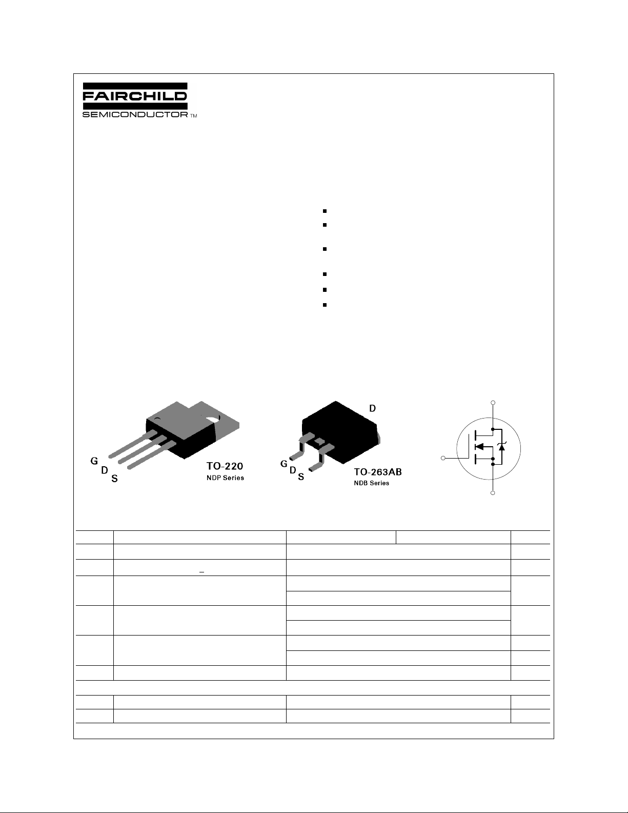
NDP7052 / NDB7052
N-Channel Enhancement Mode Field Effect Transistor
General Description Features
These N-Channel enhancement mode power field effect
transistors are produced using Fairchild's proprietary, high cell
density, DMOS technology. This very high density process has
been especially tailored to minimize on-state resistance,
provide superior switching performance, and withstand high
energy pulses in the avalanche and commutation modes.
These devices are particularly suited for low voltage
applications such as automotive, DC/DC converters, PWM
motor controls, and other battery powered circuits where fast
switching, low in-line power loss, and resistance to transients
are needed.
________________________________________________________________________________
75 A, 50 V. R
= 0.01 Ω @ VGS= 10 V.
DS(ON)
Critical DC electrical parameters specified at elevated
temperature.
Rugged internal source-drain diode can eliminate the need
for an external Zener diode transient suppressor.
175°C maximum junction temperature rating.
High density cell design for extremely low R
DS(ON)
.
TO-220 and TO-263 (D2PAK) package for both through hole
and surface mount applications.
D
G
S
Absolute Maximum Ratings T
Symbol Parameter NDP7052 NDB7052 Units
V
DSS
V
DGR
V
GSS
I
D
P
D
TJ,T
THERMAL CHARACTERISTICS
R
θJC
R
θ JA
Drain-Source Voltage 50 V
Drain-Gate Voltage (RGS < 1 MΩ)
Gate-Source Voltage - Continuous ±20 V
- Nonrepetitive (tP < 50 µs)
Drain Current - Continuous 75 A
- Pulsed 225
Total Power Dissipation @ TC = 25°C
Derate above 25°C 1 W/°C
Operating and Storage Temperature Range -65 to 175 °C
STG
Thermal Resistance, Junction-to-Case 1 °C/W
Thermal Resistance, Junction-to-Ambient 62.5 °C/W
= 25°C unless otherwise noted
C
50 V
±40
150 W
© 1997 Fairchild Semiconductor Corporation
NDP7052 Rev.B1
Page 2
Electrical Characteristics (T
= 25°C unless otherwise noted)
C
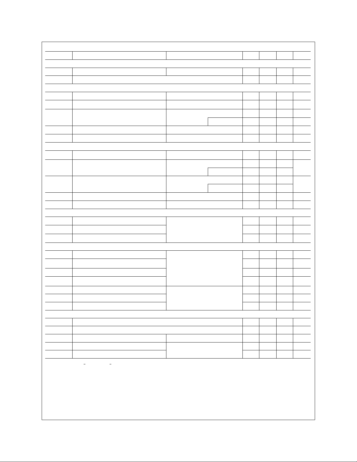
Symbol Parameter Conditions Min Typ Max Units
DRAIN-SOURCE AVALANCHE RATINGS (Note)
W
DSS
I
AR
Single Pulse Drain-Source Avalanche Energy VDD = 25 V, ID = 75 A 550 mJ
Maximum Drain-Source Avalanche Current 75 A
OFF CHARACTERISTICS
BV
∆BV
I
DSS
DSS
DSS
Drain-Source Breakdown Voltage VGS = 0 V, ID = 250 µA 50 V
Breakdown Voltage Temp. Coefficient
/∆T
J
Zero Gate Voltage Drain Current
ID = 250 µA, Referenced to 25 o C
VDS = 40 V, V
GS
= 0 V
57
10 µA
mV/oC
TJ = 125°C 1 mA
I
GSSF
I
GSSR
Gate - Body Leakage, Forward
VGS = 20 V, VDS = 0 V
Gate - Body Leakage, Reverse VGS = -20 V, VDS = 0 V -100 nA
100 nA
ON CHARACTERISTICS (Note)
∆V
V
GS(th)
GS(th)
Gate Threshold VoltageTemp. Coefficient
/∆T
J
Gate Threshold Voltage
ID = 250 µA, Referenced to 25 o C
VDS = VGS, ID = 250 µA
-5.2
mV/oC
2 2.2 3 V
TJ = 125°C 1.4 1.55 2.4
R
I
g
D(on)
DS(ON)
FS
Static Drain-Source On-Resistance
VGS = 10 V, ID = 37.5 A
TJ = 125°C
On-State Drain Current VGS = 10 V, VDS= 10 V 60 A
Forward Transconductance
VDS = 10 V, ID = 37.5 A
0.008 0.01
0.011 0.018
52 S
DYNAMIC CHARACTERISTICS
C
iss
C
oss
C
rss
Input Capacitance
Output Capacitance 1300 pF
Reverse Transfer Capacitance 460 pF
VDS = 25 V, VGS = 0 V,
f = 1.0 MHz
3400 pF
SWITCHING CHARACTERISTICS (Note)
t
t
t
t
Q
Q
Q
D(on)
r
D(off)
f
Turn - On Delay Time
Turn - On Rise Time 147 250 nS
VDD = 30 V, ID = 75 A,
VGS = 10 V, R
GEN
= 5 Ω
Turn - Off Delay Time 85 150 nS
Turn - Off Fall Time 165 300 nS
g
gs
gd
Total Gate Charge
Gate-Source Charge 12 nC
Gate-Drain Charge 46 nC
VDS = 24 V,
ID = 37.5 A, VGS = 10 V
15 30 nS
117 160 nC
DRAIN-SOURCE DIODE CHARACTERISTICS
I
S
ISM
V
t
rr
I
rr
SD
Maximum Continuos Drain-Source Diode Forward Current 75 A
Maximum Pulsed Drain-Source Diode Forward Current 225 A
Drain-Source Diode Forward Voltage VGS = 0 V, IS = 13 A (Note) 0.9 1.3 V
Reverse Recovery Time
VGS = 0 V, IF = 37.5 A,
75 150 ns
Reverse Recovery Current dIF/dt = 100 A/µs 4 10 A
Note: Pulse Test: Pulse Width < 300 µs, Duty Cycle < 2.0%.
Ω
NDP7052 Rev.B1
Page 3
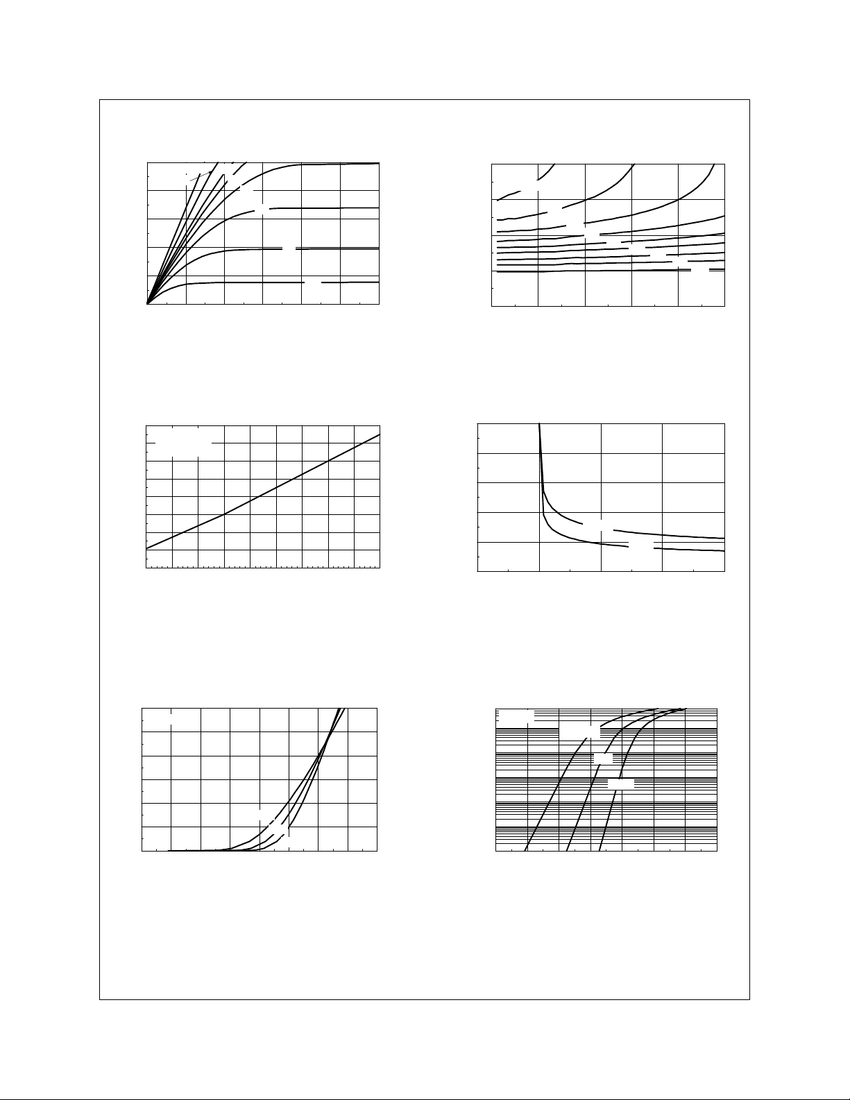
Typical Electrical Characteristics
100
V = 10V
GS
80
60
40
20
D
I , DRAIN-SOURCE CURRENT (A)
0
0 0.5 1 1.5 2 2.5 3
6.0
7.0
5.5
5.0
4.5
V , DRAIN-SOURCE VOLTAGE (V)
DS
4.0
3.5
Figure 1. On-Region Characteristics.
2
I =37.5A
D
1.8
V = 10V
GS
1.6
1.4
1.2
1
DS(ON)
R , NORMALIZED
0.8
0.6
DRAIN-SOURCE ON-RESISTANCE
0.4
-50 -25 0 25 50 75 100 125 150 175
T , JUNCTION TEMPERATURE (°C)
J
2.5
V =4.0V
GS
2
4.5
5.0
1.5
DS(on)
R , NORMALIZED
1
DRAIN-SOURCE ON-RESISTANCE
0.5
0 20 40 60 80 100
5.5
6.0
6.5
I , DRAIN CURRENT (A)
D
7.0
Figure 2. On-Resistance Variation
with Drain Current and Gate Voltage.
0.05
0.04
0.03
0.02
0.01
DS(ON)
R , ON-RESISTANCE (OHM)
0
2 4 6 8 10
V , GATE TO SOURCE VOLTAGE (V)
GS
125°C
25°C
8.0
10.0
ID=37.5A
Figure 3. On-Resistance Variation
with Temperature.
60
V = 10V
DS
50
40
30
20
D
I , DRAIN CURRENT (A)
10
0
1 1.5 2 2.5 3 3.5 4 4.5 5
V , GATE TO SOURCE VOLTAGE (V)
T = -55°C
J
25°C
125°C
GS
Figure 5. Transfer Characteristics.
Figure 4. On Resistance Variation with
Gate-To- Source Voltage.
60
V =0V
GS
10
5
1
0.5
0.1
0.01
0.001
S
I , REVERSE DRAIN CURRENT (A)
0.0001
0 0.2 0.4 0.6 0.8 1 1.2 1.4
T = 125°C
J
25°C
-55°C
V , BODY DIODE FORWARD VOLTAGE (V)
SD
Figure 6. Body Diode Forward Voltage
Variation with Source Current and Temperature.
NDP7052 Rev.B1
Page 4
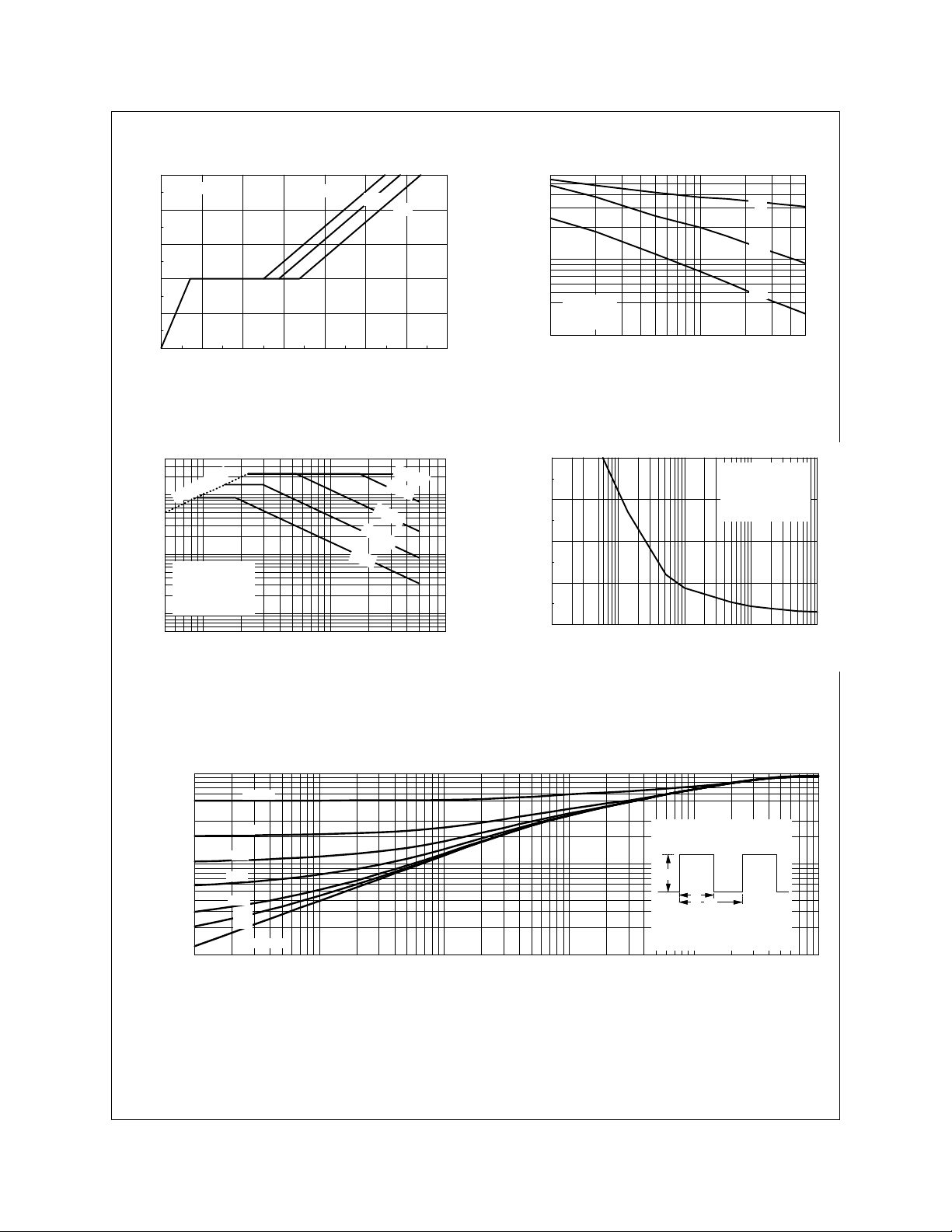
Typical Electrical Characteristics (continued)
10
I = 37.5A
D
8
6
4
2
GS
V , GATE-SOURCE VOLTAGE (V)
0
0 20 40 60 80 100 120 140
Q , GATE CHARGE (nC)
V = 12V
DS
g
24V
48V
Figure 7. Gate Charge Characteristics.
400
200
DS(ON)
100
R Limit
50
20
10
V = 10V
GS
5
SINGLE PULSE
D
I , DRAIN CURRENT (A)
2
1
0.5
0.5 1 3 5 10 20 30 80
o
R = 1 C/W
JC
θ
T = 25 °C
C
V , DRAIN-SOURCE VOLTAGE (V))
DS
100µs
1ms
10ms
100ms
DC
6000
C
iss
2000
C
1000
CAPACITANCE (pF)
500
f = 1 MHz
V = 0V
GS
200
1 5 10 20 50
V , DRAIN TO SOURCE VOLTAGE (V)
DS
oss
C
rss
Figure 8.Capacitance Characteristics.
2000
1500
1000
POWER (W)
500
0
0.1 0.3 1 3 10 30 100 300 1,000
SINGLE PULSE TIME (mS)
SINGLE PULSE
R =1° C/W
JC
θ
T = 25°C
C
Figure 9. Maximum Safe Operating Area.
1
0.5
0.3
0.2
0.1
0.05
0.03
0.02
r(t), NORMALIZED EFFECTIVE
TRANSIENT THERMAL RESISTANCE
0.01
0.01 0.05 0.1 0.5 1 5 10 50 100 500 1000
D = 0.5
0.2
0.1
0.05
0.02
0.01
Single Pulse
Figure 11. Transient Thermal Response Curve.
t ,TIME (ms)
1
Figure 10. Single Pulse Maximum
Power Dissipation.
R (t) = r(t) * R
JC
θ
R = 1°C/W
JC
θ
P(pk)
t
1
t
2
T - T = P * R (t)
CJ
Duty Cycle, D = t /t
JC
θ
JC
θ
1
2
NDP7052 Rev.B1
Page 5

NDP7052 Rev.B1
Page 6

NDP7052 Rev.B1
 Loading...