

Page 1
INTEGRATED CIRCUITS
74F670
4 x 4 register file (3-State)
Product specification
IC15 Data Handbook
1990 Jul 12
Page 2
Philips Semiconductors Product specification
74F6704 x 4 register file (3-State)
FEA TURES
•Simultaneous and Independent Read and Write operations
•Expandable to almost any word size and bit length
•3-State outputs
DESCRIPTION
The 74F670 is a 16-bit 3-State Register File organized as 4 words of
4 bits each. Separate Read and Write Address and Enable inputs
are available, permitting simultaneous writing into one word location
and reading from another location. The 4-bit word to be stored is
presented to four data inputs.
The Write address inputs (WA and WB) determine the location of the
stored word. The Write Address inputs should only be changed
when the Write Enable input (WE
operation. When the WE
is Low, the data is entered into the
addressed location.
The addressed location remains transparent to the data while the
WE
is Low. Data supplied at the inputs will be read out in true
(non-inverting) form from the 3-State outputs. Data and address
inputs are inhibited when the WE is High. Direct acquisition of data
stored in any of the four registers is made possible by individual
Read Address inputs (RA, RB). The addressed word appears at the
four outputs when the Read Enable (RE
the high impedance “off” state when the RE
outputs to be tied together to increase the word capacity to very
large numbers.
Up to 128 devices can be stacked to increase the word size to 512
locations by tying the 3-State outputs together. Since the limiting
factor for expansion is the output High current, further stacking is
possible by tying pullup reisistors to the outputs to increase the I
current available. Design of the Read Enable signals for the stacked
devices must ensure that there is no overlap in the Low levels which
cause more than one output to be active at the same time. Parallel
expansion to generate n-bit words is accomplished by driving the
Enable and address inputs of each device in parallel.
) is High for conventional
) is Low. Data outputs are in
is High. This permits
OH
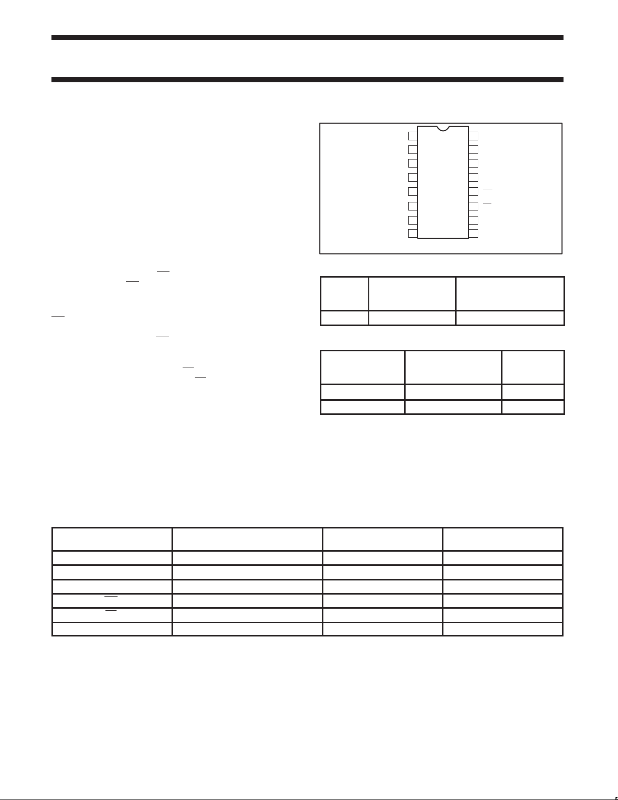
PIN CONFIGURATION
1
D1
2
D2
3
D3
4
RB
5
RA
Q3
6
7
Q2
GND
8
TYPICAL
TYPE
PROPAGATION
DELAY
74F670 6.5ns 50mA
V
16
CC
15
D0
14
WA
13
WB
12
WE
11
RE
10
Q0
Q1
9
SF01178
TYPICAL
SUPPLY CURRENT
(TOTAL)
ORDERING INFORMATION
COMMERCIAL RANGE
DESCRIPTION
16-pin plastic DIP N74F670N SOT38-4
16-pin plastic SOL N74F670D SOT162-1
VCC = 5V ±10%,
T
= 0°C to +70°C
amb
PKG DWG #
INPUT AND OUTPUT LOADING AND FAN-OUT TABLE
PINS DESCRIPTION
74F(U.L.)
HIGH/LOW
D0 - D3 Data inputs 1.0/1.0 20µA/0.6mA
WA, WB Write address inputs 1.0/1.0 20µA/0.6mA
RA, RB Read address inputs 1.0/1.0 20µA/0.6mA
WE Write Enable inputs 1.0/1.0 20mA/0.6mA
RE Read Enable inputs 1.0/1.0 20mA/0.6mA
Q0–Q3 Data output 150/40 3.0mA/24mA
NOTE:
One (1.0) FAST Unit Load is defined as: 20µA in the High state and 0.6mA in the Low state.
1990 Jul 12 853-0014 99965
2
LOAD VALUE
HIGH/LOW
Page 3
Philips Semiconductors Product specification
OPERATING MODE
Read
OPERATING MODE
Write data
74F6704 x 4 register file (3-State)
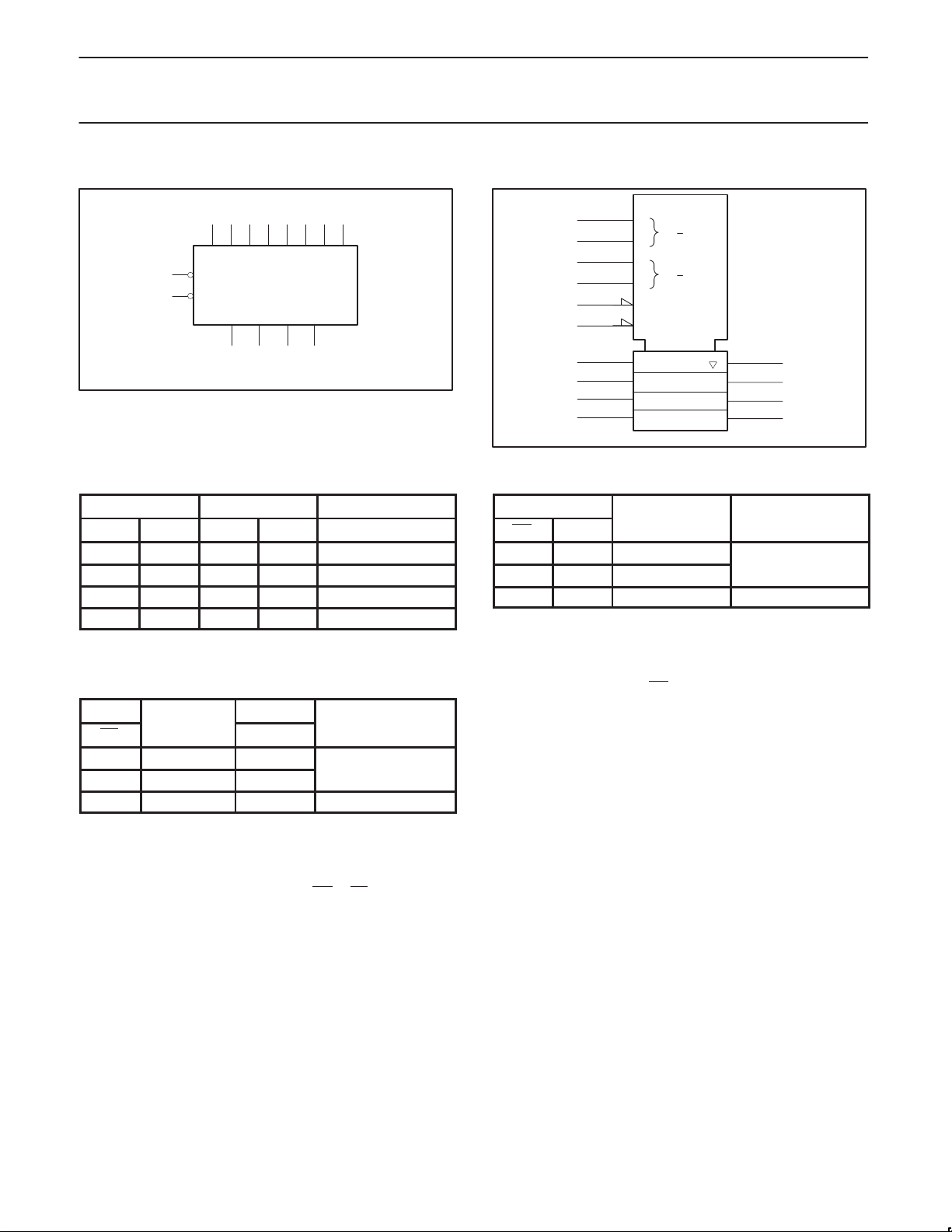
LOGIC SYMBOL
14 13 5 4 15 1 2 3
WA WB RA RB D0 D1 D2 D3
WE
12
RE
11
Q3Q2
76
SF01179
V
=Pin 16
CC
GND=Pin 8
Q1Q0
10 9
WORD SELECT FUNCTION TABLE
WRITE MODE READ MODE OPERATING MODE
WB WA RB RA Word Selected
L L L L W ord 0
L H L H Word 1
H L H L Word 2
H H H H Word 3
H = High voltage level
L = Low voltage level
READ MODE FUNCTION TABLE
INPUT
RE
INTERNAL
LATCHES*
L L L
L H H
H X Z Disabled
H = High voltage level
L = Low voltage level
X = Don’t care
Z = High impedance “off” state
* = The selection of “internal latches” by Read Address
(RA and RB) are not constrained by WE
OUTPUT
Qn
or RE operation.
LOGIC SYMBOL (IEEE/IEC)
14
13
5
4
12
11
15
1
2
3
RAM 4X4
0
0
1A
3
1
0
0
2A
3
1
C4 [WRITE]
EN [READ]
1A, 4D
10
2A
9
7
6
SF01180
WRITE MODE FUNCTION TABLE
INPUTS
WE Dn
L L L
L H H
H X NC Data latched
H = High voltage level
L = Low voltage level
NC= No change
X = Don’t care
* = The write address (WA and WB) to the “internal latches”
must be stabled while WE
INTERNAL
LATCHES*
is Low for conventional operation.
1990 Jul 12
3
Page 4
Philips Semiconductors Product specification
74F6704 x 4 register file (3-State)
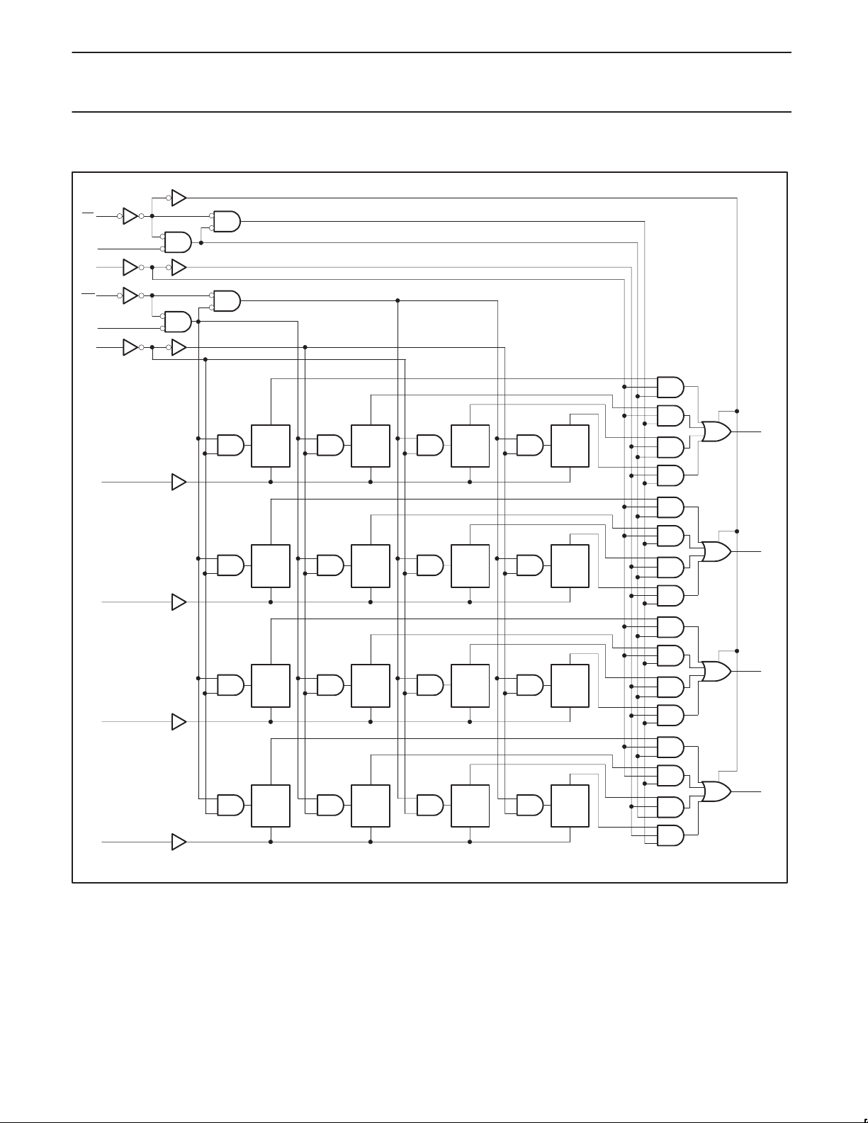
LOGIC DIAGRAM
11
RE
5
RA
4
RB
12
WE
13
WB
14
WA
6
Q
E
D
3
D3
Q
E
D
Q
E
D
Q
E
D
Q3
2
D2
1
D1
15
D0
V
=Pin 16
CC
GND=Pin 8
7
9
10
SF01181
Q2
Q1
Q0
Q
E
D
Q
E
D
Q
E
D
Q
E
D
Q
E
D
Q
E
D
Q
E
D
Q
E
D
Q
E
D
Q
E
D
Q
E
D
Q
E
D
1990 Jul 12
4
Page 5

Philips Semiconductors Product specification
SYMBOL
PARAMETER
UNIT
NO TAG
VOHHigh-level output voltage
V
VOLLow-level output voltage
V
74F6704 x 4 register file (3-State)
ABSOLUTE MAXIMUM RATINGS
(Operation beyond the limits set forth in this table may impair the useful life of the device.
Unless otherwise noted these limits are over the operating free-air temperature range.)
SYMBOL PARAMETER RATING UNIT
V
CC
V
IN
I
IN
V
OUT
I
OUT
T
amb
T
stg
RECOMMENDED OPERATING CONDITIONS
V
CC
V
IH
V
IL
I
IK
I
OH
I
OL
T
amb
Supply voltage –0.5 to +7.0 V
Input voltage –0.5 to +7.0 V
Input current –30 to +5 mA
Voltage applied to output in High output state –0.5 to V
CC
V
Current applied to output in Low output state 48 mA
Operating free-air temperature range 0 to +70 °C
Storage temperature –65 to +150 °C
LIMITS
MIN NOM MAX
Supply voltage 4.5 5.0 5.5 V
High-level input voltage 2.0 V
Low-level input voltage 0.8 V
Input clamp current –18 mA
High-level output current –3
mA
Low-level output current 24 mA
Operating free-air temperature range 0 70 °C
DC ELECTRICAL CHARACTERISTICS
(Over recommended operating free-air temperature range unless otherwise noted.)
LIMITS
SYMBOL PARAMETER TEST CONDITIONS
VCC = MIN, VIL = MAX
VIH = MIN, IOH = MAX
VCC = MIN, VIL = MAX
VIH = MIN, IOL = MAX
IK
VCC = MAX, V
VCC = MAX, V
= 2.7V 50 µA
O
= 0.5V –50 µA
O
VCC = MAX –60 –150 mA
VCC = MAX
V
I
I
I
IH
I
IL
I
OZH
I
OZL
I
OS
I
CC
p
p
IK
Input clamp voltage VCC = MIN, II = I
Input current at maximum input voltage VCC = MAX, VI = 7.0V 100 µA
High-level input current VCC = MAX, VI = 2.7V 20 µA
Low-level input current VCC = MAX, VI = 0.5V –0.6 mA
Off state output current,
High-level voltage applied
Off state output current,
Low-level voltage applied
Short-circuit output current
Supply current (total)
NO TAG
I
CCH
I
CCL
I
CCZ
±10%V
±5%V
±10%V
±5%V
CC
CC
CC
CC
MIN
2.4
2.7 3.4
TYP
NO TAG
MAX
0.35 0.50
0.35 0.50
–0.73 –1.2 V
50 70 mA
50 70 mA
55 80 mA
NOTES:
1. For conditions shown as MIN or MAX, use the appropriate value specified under recommended operating conditions for the applicable type.
2. All typical values are at V
3. Not more than one output should be shorted at a time. For testing I
= 5V, T
CC
techniques are preferable in order to minimize internal heating and more accurately reflect operational values. Otherwise, prolonged shorting
amb
= 25°C.
, the use of high-speed test apparatus and/or sample-and-hold
OS
UNIT
1990 Jul 12
5
Page 6

Philips Semiconductors Product specification
TEST
V
0V
V
10%
,
CONDITION
C
L
50pF,
C
L
50pF,
74F6704 x 4 register file (3-State)
of a High output may raise the chip temperature well above normal and thereby cause invalid readings in other parameter tests. In any
sequence of parameter tests, I
tests should be performed last.
OS
AC ELECTRICAL CHARACTERISTICS
LIMITS
T
SYMBOL PARAMETER
= +25°C
amb
= +5.
CC
C
= 50pF,
=
R
= 500Ω
L
T
= 0°C to +70°C
amb
= +5.0V ±
CC
C
= 50pF
=
RL = 500Ω
UNIT
MIN TYP MAX MIN MAX
t
t
t
t
t
t
t
t
t
t
PLH
PHL
PLH
PHL
PLH
PHL
PZH
PZL
PHZ
PLZ
Propagation delay
RA, RB to Qn
Propagation delay
WE
to Qn
Propagation delay
Dn to Qn
RE Enable time
Qn to High or Low level
RE Disable time
Qn to High or Low level
Waveform 3, 4
Waveform 1, 2
Waveform 1, 2
Waveform 5
Waveform 6
Waveform 5
Waveform 6
3.5
4.0
5.0
6.5
3.5
6.0
3.0
4.5
2.0
3.0
5.5
5.5
7.0
8.5
6.0
8.0
7.0
6.5
3.0
5.0
9.0
8.5
10.0
11.5
8.5
11.0
12.0
9.0
6.5
8.5
3.0
3.5
4.5
6.0
3.0
5.5
2.5
4.0
1.5
3.0
10.0
9.9
11.0
12.5
9.5
12.5
13.0
10.0
7.5
8.5
ns
ns
ns
ns
ns
ns
ns
ns
ns
ns
AC SETUP REQUIREMENTS
LIMITS
T
= +25°C T
SYMBOL PARAMETER TEST CONDITION
amb
VCC = +5.0V VCC = +5.0V ± 10%
CL = 50pF, RL = 500Ω CL = 50pF, RL = 500Ω
MIN TYP MAX MIN MAX
ts(H)
ts(L)
th(H)
t
(L)
h
ts(H)
ts(L)
th(H)
th(L)
Setup time, High or Low
Dn to positive going WE
Hold time, High or Low
Dn to positive going WE
Setup time, High or Low
WA, WB to negative going WE
Hold time, High or Low
WA, WB to negative going WE
1
1
Waveform 3, 4
Waveform 3, 4
Waveform 3, 4
Waveform 3, 4
1.5
6.0
0
1.0
0
0
0
0
tw(L) WE Pulse width, Low Waveform 3, 4 6.5 8.5 ns
NOTES:
1. Write Address (WA, WB) setup time will protect the data written into the previous address. If protection of data in the previous address is not
required, setup time for Write Address to WE
time for Write Address to WE
will result in data being written into that location.
can be ignored. Any address selection sustained for the final 7ns of the WE pulse during hold
= 0°C to +70°C
amb
1.5
7.0
0
1.0
0
0
0
0
UNIT
ns
ns
ns
ns
ns
ns
ns
ns
1990 Jul 12
6
Page 7

Philips Semiconductors Product specification
74F6704 x 4 register file (3-State)
AC WAVEFORMS
For all waveforms, VM=1.5V.
The shaded areas indicate when the input is permitted to change for predictable output performance.
V
Dn
WE
Qn
M
t
PLH
V
M
Waveform 1. Propagation Delay, Write Enable
and Data to Outptus
WA, WB
Dn
WE
V
M
t
s
V
t
tw(L)
V
M
V
t
PHL
M
V
M
t
PLH
V
M
V
M
SF01183
Dn
V
M
t
PHL
V
M
WE
Qn
SF01182
Waveform 2. Propagation Delay, Write Enable
and Data to Outputs
V
M
t
h
V
M
M
t
s
h
V
M
RA, RB
Qn
Qn
t
PHL
t
PLH
V
M
V
V
V
M
V
M
M
M
t
PLH
V
M
t
PHL
V
M
SF01184
Waveform 3. Setup and Hold Times for Write Address to Write
Enable and Data to Write Enable
Qn
RE
V
M
t
PZH
V
M
t
PHZ
V
M
VOH -0.3V
0V
SF01186
Waveform 5. 3-State Output Enable Time to High Level and
Output Disable Time from High Level
SF01185
Waveform 4. Propagation Delays for Read Address to Output
RE
Qn
V
M
t
PZL
V
V
M
t
PLZ
M
+0.3V
V
OL
SF01187
Waveform 6. 3-State Output Enable Time to Low Level and
Output Disable Time from Low Level
1990 Jul 12
7
Page 8

Philips Semiconductors Product specification
74F6704 x 4 register file (3-State)
TEST CIRCUIT AND WAVEFORM
V
V
PULSE
GENERATOR
IN
R
Test Circuit for 3-State Outputs
SWITCH POSITION
TEST SWITCH
t
t
PLZ
PZL
closed
closed
All other open
T
D.U.T.
CC
V
OUT
7.0V
R
L
C
R
L
L
NEGATIVE
PULSE
POSITIVE
PULSE
90%
10%
V
M
10%
t
THL (tf
t
TLH (tr
90%
V
M
Input Pulse Definition
t
w
V
M
10%
)
)
t
)
TLH (tr
t
)
THL (tf
90%
V
M
t
w
90%
10%
AMP (V)
0V
AMP (V)
0V
DEFINITIONS:
= Load resistor;
R
L
see AC electrical characteristics for value.
C
= Load capacitance includes jig and probe capacitance;
L
see AC electrical characteristics for value.
R
= Termination resistance should be equal to Z
T
pulse generators.
OUT
of
family
74F
INPUT PULSE REQUIREMENTS
V
amplitude
3.0V
M
1.5V
rep. rate
1MHz 500ns
t
w
t
TLHtTHL
2.5ns 2.5ns
SF00777
1990 Jul 12
8
Page 9

Philips Semiconductors Product specification
74F670Register file
DIP16: plastic dual in-line package; 16 leads (300 mil) SOT38-4
1990 Jul 12
9
Page 10

Philips Semiconductors Product specification
74F670Register file
SO16: plastic small outline package; 16 leads; body width 7.5 mm SOT162-1
1990 Jul 12
10
Page 11

Philips Semiconductors Product specification
74F670Register file
NOTES
1990 Jul 12
11
Page 12

Philips Semiconductors Product specification
74F670Register file
Data sheet status
Data sheet
status
Objective
specification
Preliminary
specification
Product
specification
Product
status
Development
Qualification
Production
Definition
This data sheet contains the design target or goal specifications for product development.
Specification may change in any manner without notice.
This data sheet contains preliminary data, and supplementary data will be published at a later date.
Philips Semiconductors reserves the right to make chages at any time without notice in order to
improve design and supply the best possible product.
This data sheet contains final specifications. Philips Semiconductors reserves the right to make
changes at any time without notice in order to improve design and supply the best possible product.
[1]
[1] Please consult the most recently issued datasheet before initiating or completing a design.
Definitions
Short-form specification — The data in a short-form specification is extracted from a full data sheet with the same type number and title. For
detailed information see the relevant data sheet or data handbook.
Limiting values definition — Limiting values given are in accordance with the Absolute Maximum Rating System (IEC 134). Stress above one
or more of the limiting values may cause permanent damage to the device. These are stress ratings only and operation of the device at these or
at any other conditions above those given in the Characteristics sections of the specification is not implied. Exposure to limiting values for extended
periods may affect device reliability.
Application information — Applications that are described herein for any of these products are for illustrative purposes only. Philips
Semiconductors make no representation or warranty that such applications will be suitable for the specified use without further testing or
modification.
Disclaimers
Life support — These products are not designed for use in life support appliances, devices or systems where malfunction of these products can
reasonably be expected to result in personal injury . Philips Semiconductors customers using or selling these products for use in such applications
do so at their own risk and agree to fully indemnify Philips Semiconductors for any damages resulting from such application.
Right to make changes — Philips Semiconductors reserves the right to make changes, without notice, in the products, including circuits, standard
cells, and/or software, described or contained herein in order to improve design and/or performance. Philips Semiconductors assumes no
responsibility or liability for the use of any of these products, conveys no license or title under any patent, copyright, or mask work right to these
products, and makes no representations or warranties that these products are free from patent, copyright, or mask work right infringement, unless
otherwise specified.
Philips Semiconductors
811 East Arques Avenue
P.O. Box 3409
Sunnyvale, California 94088–3409
Telephone 800-234-7381
Copyright Philips Electronics North America Corporation 1998
All rights reserved. Printed in U.S.A.
print code Date of release: 10-98
Document order number: 9397-750-05172
yyyy mmm dd
12
 Loading...