

Page 1

INTEGRATED CIRCUITS
74F657
Octal transceiver with 8-bit parit
generator/checker
Process specification
IC15 Data Handbook
1990 Jul 30
Page 2
Philips Semiconductors Product specification
74F657Octal transceiver with 8-bit parity generator/checker
FEA TURES
• Combines 74F245 and 74F280A functions in one package
• High impedance base input for reduced loading (70µA in
high and low states)
• Ideal in applications where high output drive and light bus
loading are required (I
is 70µA vs FAST std of 600µA)
IL
• 3–state buffer outputs sink 64mA and source 15mA
• Input diodes for termination effects
• 24–pin plastic slim DIP (300mil) package
• Industrial temperature range available (–40°C to +85°C)
DESCRIPTION
The 74F657 is an octal transceiver featuring non–inverting
buffers with 3–state outputs and an 8–bit parity
generator/checker, and is intended for bus–oriented
applications. The buffers have a guaranteed current sinking
capability of 24mA at the A ports and 64mA at the B ports.
The transmit/receive (T/R
the data flow through the bidirectional transceivers.
Transmit (active high) enables data from A ports to B ports;
receive (active low) enables data from B ports to A ports.
The output enable (OE) input disables both the A and B ports by
placing them in a high impedance condition when the OE
.
high
) input determines the direction of
input is
The parity select (ODD/EVEN) input gives the user the option of
odd or even parity systems
The parity (PARITY) pin is an output from the generator/checker
when transmitting from the port A to B (T/R
when receiving from port B to A port ( T/R
When transmitting (T/R
is set, then the A port data is polled to determined the number of
high bits. The parity (PARITY) output then goes to the logic state
determined by the parity select (ODD/EVEN
number of high bits on port A.
For example, if the parity select (ODD/EVEN
parity), and the number of high bits on port A is odd, then the parity
(PARITY) output will be high, transmitting even parity. If the number
of high bits on port A is even, then the parity (PARITY) output will
be low, keeping even parity.
When in receive mode (T/R
the number of high bits. If parity select (ODD/EVEN
parity) and the number of highs on port B is:
(1) odd and the parity (PARITY) input is high, then ERROR
high, significantly no error.
(2) even and the parity (PARITY) input is high, then ERROR
asserted low, indicating an error.
TYPE
74F657 8.0ns 100mA
TYPICAL PROPAGA-
TION DELAY
.
= high) and an input
= low).
= high) the parity select (ODD/EVEN) input
) setting and by the
) is set low (even
= low) the B port is polled to determine
) is low (even
will be
will be
TYPICAL SUPPL Y
CURRENT( TOTAL)
ORDERING INFORMATION
ORDER CODE
COMMERCIAL RANGE INDUSTRIAL RANGE
DESCRIPTION
24–pin plastic slim
DIP (300mil)
24–pin plastic SOL N74F657D I74F657D SOT137-1
24–pin plastic SSOP N74F657DB I74F657DB SOT340-1
VCC = 5V ±10%, VCC = 5V ±10%,
T
= 0°C to +70°C T
amb
N74F657N I74F657N SOT222-1
= –40°C to +85°C
amb
PKG DWG #
INPUT AND OUTPUT LOADING AND FAN OUT TABLE
PINS DESCRIPTION
A0 – A7 A ports 3–state inputs 3.5/0.1 17
B0 – B7 B ports 3–state inputs 3.5/0.1 17
PARITY Parity input 3.5/0.1 17
T/R Transmit/receive input 2.0/0.066
ODD/EVEN Parity select input 1.0/0.033
OE Output enable input (active low) 2.0/0.066
A0 – A7 A ports 3–state outputs 150/40 3.0mA/24mA
B0 – B7 B ports 3–state outputs 750/106.7 15mA/64mA
PARITY Parity output 750/106.7 15mA/64mA
ERROR Error output 750/106.7
Note to input and output loading and fan out table
1. One (1.0) FAST unit load is defined as: 20µA in the high state and 0.6mA in the low state.
74F (U.L.)
HIGH/LOW
LOAD VALUE
HIGH/LOW
70µA/70µA
70µA/70µA
70µA/70µA
40µA/40µA
20µA/20µA
40µA/40µA
15mA/64mA
90 July 30 853 1117 00081
2
Page 3
Philips Semiconductors Product specification
74F657Octal transceiver with 8-bit parity generator/checker
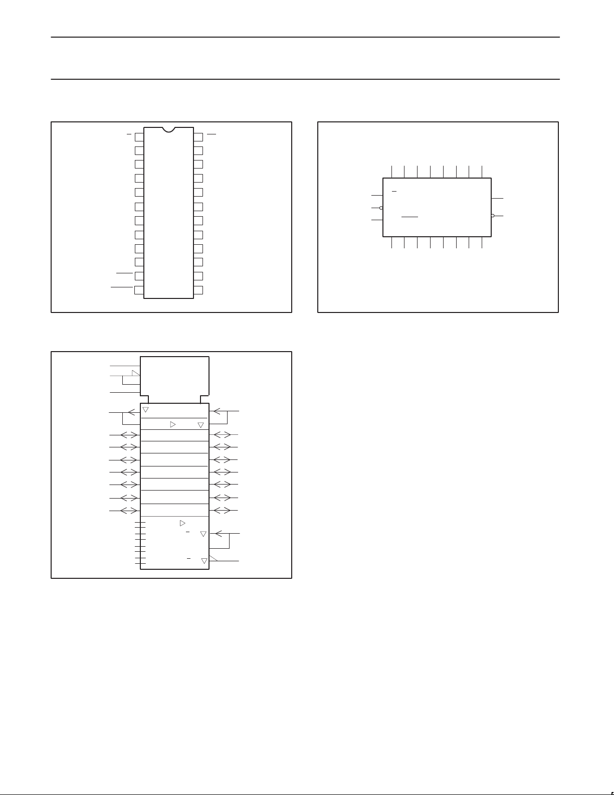
PIN CONFIGURATION
T/R
1OE
2
A0
3
A1
4
A2
5
A3
6
A4
V
7
CC
A5
8
A6
9
A7
10
ODD/EVEN
11
ERROR
IEC/IEEE SYMBOL
24
1
11
2
3
4
5
6
8
9
10
3 EN1/3G5 (REC)
3 EN2 (XMIT)
N4
Z11
G3
LOGIC SYMBOL
24
23
B0
22
B1
21
B2
20
B3
GND
19
GND
18
17
B4
16
B5
15
B6
14
B7
PARITY
1312
SF00414
5
23
22
21
20
17
16
15
14
13
12
SF00416
1
2
11
2 k
.
.
.
18
4, 2
4, 1
= Pin 7
V
CC
GND = Pin 18, 19
234568910
A0 A1 A2 A3 A4 A5 A6 A7
T/R
1
OE
24
ODD/EVEN
11
B0 B1 B2 B3
23 22 21 20 17 16 15 14
PARITY
ERROR
B4 B5 B6 B7
13
12
SF00415
90 July 30
3
Page 4
Philips Semiconductors Product specification
74F657Octal transceiver with 8-bit parity generator/checker
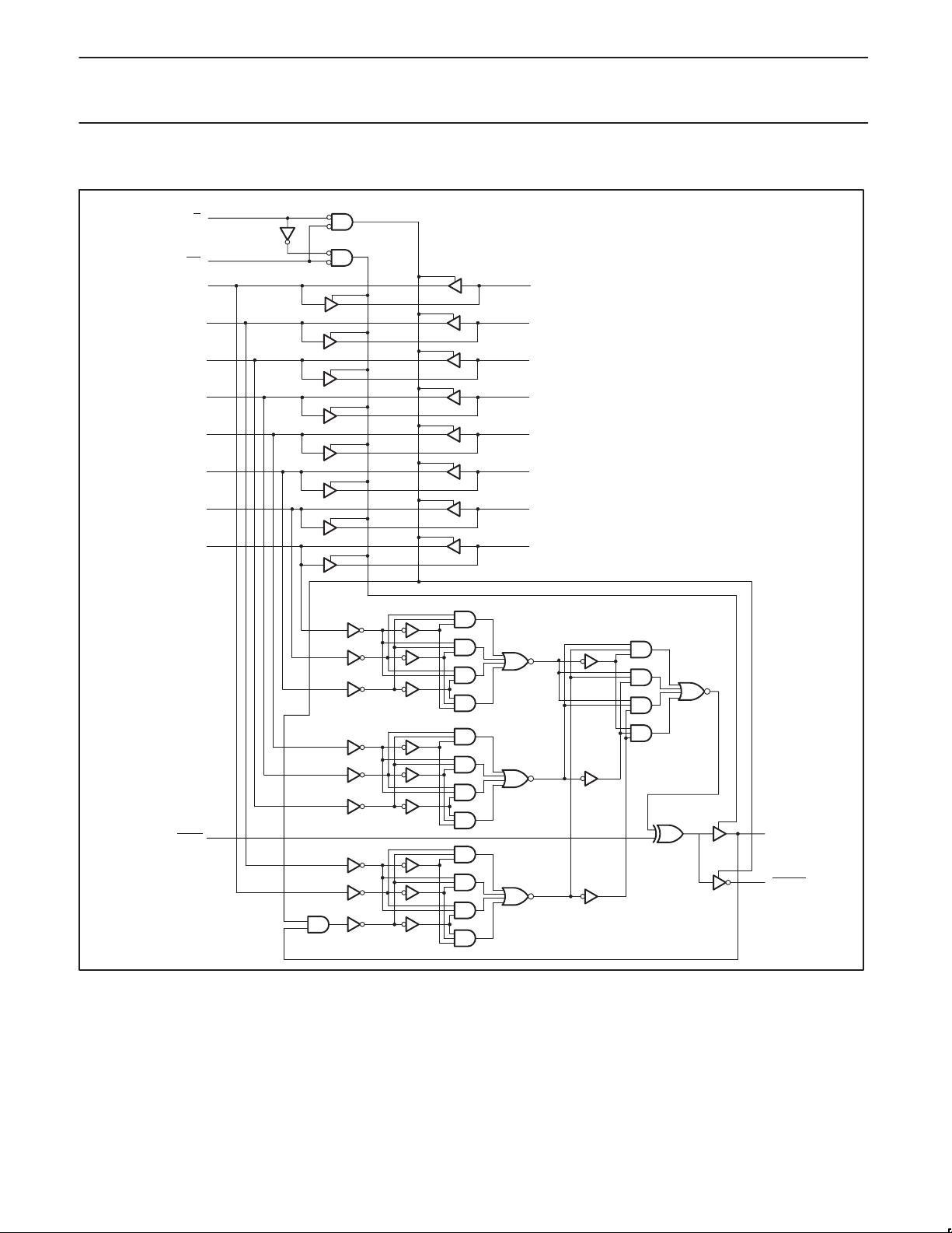
LOGIC DIAGRAM
1
T/R
24
OE
2
A0
23
B0
3
A1
4
A2
5
A3
6
A4
8
A5
9
A6
10
A7
22
B1
21
B2
20
B3
17
B4
16
B5
15
B6
14
B7
VCC = Pin 7,
GND = Pin 18, 19
90 July 30
ODD/EVEN
11
13
12
PARITY
ERROR
SF00417
4
Page 5

Philips Semiconductors Product specification
74F657Octal transceiver with 8-bit parity generator/checker
FUNCTION TABLE
NUMBER OF INPUTS THAT ARE HIGH INPUTS INPUT/OUTPUT OUTPUTS
OE T/R ODD/EVEN PARITY ERROR OUTPUTS MODE
L
0, 2, 4, 6, 8
1, 3, 5, 7
Don’t care H X X Z Z Z
Notes to function table
1. H = High voltage level
2. L = Low voltage level
3. X = Don’t care
4. Z = High impedance ”’off” state
H
L
H
L
L
L
L
L
L
L
L
L
H
L
H
L
L
L
L
L
L
L
L
H
L
H
H
L
L
H
L
H
H
L
L
H
L
H
L
H
L
L
H
H
L
H
L
Z
Z
H
L
L
H
Z
Z
L
H
H
L
Transmit
Transmit
Receive
Receive
Receive
Receive
Transmit
Transmit
Receive
Receive
Receive
Receive
ABSOLUTE MAXIMUM RATINGS
(Operation beyond the limit set forth in this table may impair the useful life of the device. Unless otherwise noted these limits are over the
operating free air temperature range.)
SYMBOL
V
CC
V
IN
I
IN
V
OUT
I
OUT
T
amb
Supply voltage –0.5 to +7.0 V
Input voltage –0.5 to +7.0 V
Input current –30 to +5 mA
Voltage applied to output in high output state –0.5 to V
Current applied to output in low output state A0 – A7 48 mA
Operating free air temperature range Commercial range 0 to +70
PARAMETER RATING UNIT
CC
B0 – B7, PARITY, ERROR 128 mA
Industrial range –40 to +85
T
stg
Storage temperature range –65 to +150
RECOMMENDED OPERATING CONDITIONS
SYMBOL PARAMETER LIMITS UNIT
MIN NOM MAX
V
V
V
I
I
I
T
CC
IH
IL
Ik
OH
OL
amb
Supply voltage 4.5 5.0 5.5 V
High–level input voltage 2.0 V
Low–level input voltage 0.8 V
Input clamp current –18 mA
High–level output current A0 – A7 –3 mA
B0 – B7, PARITY, ERROR –15 mA
Low–level output current A0 – A7 24 mA
B0 – B7, PARITY, ERROR 64 mA
Operating free air temperature range Commercial range 0 +70
Industrial range –40 +85
V
°C
°C
°C
°C
°C
90 July 30
5
Page 6

Philips Semiconductors Product specification
74F657Octal transceiver with 8-bit parity generator/checker
DC ELECTRICAL CHARACTERISTICS
(Over recommended operating free-air temperature range unless otherwise noted.)
SYMBOL
V
OH
V
OL
V
IK
High-level output voltage B0 – B7, VIL = MAX, IOH = –12mA
Low-level output voltage B0 – B7, VIL = MAX, IOL = 48mA
Input clamp voltage VCC = MIN, II = I
Input current at
I
I
I
IH
I
IL
I
OZH
I
OZL
I
OZH
I
OZL
I
OS
I
CC
maximum input voltage A0 – A7 VCC = 5.5V, VI = 5.5V 2 mA
High–level input current VCC = MAX, VI = 2.7V 40
Low–level input current OOD/EVEN VCC = MAX, VI = 0.5V –20 µA
Off–state output current,
+ I
IH
high–level voltage applied
Off–state output current,
+ I
IL
low–level voltage applied
Off–state output current,
High–level voltage applied
Off–state output current,
low–level voltage applied
Short circuit output current
Supply current (total) I
Notes to DC electrical characteristics
1. For conditions shown as MIN or MAX, use the appropriate value specified under recommended operating conditions for the applicable type.
2. All typical values are at V
3. Not more than one output should be shorted at a time. For testing IOS, the use of high-speed test apparatus and/or sample-and-hold
techniques are preferable in order to minimize internal heating and more accurately reflect operational values. Otherwise, prolonged shorting
of a high output may raise the chip temperature well above normal and thereby cause invalid readings in other parameter tests. In any
sequence of parameter tests, I
4. For commercial range.
5. For industrial range.
PARAMETER TEST LIMITS UNIT
4,5
4,5
1
±10%V
5
±10%V
4
±10%V
±5%V
±10%V
4
±10%V
5
±5%V
4
±5%V
MIN TYP2MAX
2.4 V
CC
2.7 V
CC
2.0 V
CC
2.0 V
CC
2.0 V
CC
2.0 V
CC
CC
CC
CC
CC
CC
0.35 0.50 V
0.35 0.50 V
0.38 0.55 V
0.42 0.55 V
0.42 0.55 V
–0.73 -1.2 V
CONDITIONS
All outputs IOH = –3mA
VCC = MIN, ±5%V
PARITY, VIH = MIN ±5%V
ERROR IOH = –15mA
A0 – A7 IOL = 24mA
VCC = MIN, ±5%V
PARITY, VIH = MIN IOL = 48mA
ERROR IOL = 64mA
IK
OE, T/R,
ODD/EVEN
VCC = 0.0V, VI = 7.0V 100 µA
B0 – B7 1 mA
80
4
5
4
5
OOD/EVEN 20
OE, T/R 40
OE, T/R –40 µA
A0 – A7,
B0 – B7,
VCC = MAX, V
= 2.7V 70
O
PARITY VCC = MAX, VO = 0.5V –70
ERROR VCC = MAX, V
= 2.7V 50
O
VCC = MAX, VO = 0.5V –50
3
A0 – A7 VCC = MAX -60 -150 mA
B0 – B7 -100 -225 mA
I
CCH
90 1254mA
90 1355mA
CCL
VCC = MAX 106 1504mA
106 1605mA
= 5V, T
CC
OS
= 25°C.
amb
tests should be performed last.
I
CCZ
98 145 mA
µA
µA
µA
µA
µA
µA
µA
µA
90 July 30
6
Page 7

Philips Semiconductors Product specification
74F657Octal transceiver with 8-bit parity generator/checker
AC ELECTRICAL CHARACTERISTICS
LIMITS
T
= +25°C
amb
SYMBOL PARAMETER TEST VCC = +5.0V
CONDITION CL = 50pF,
RL = 500Ω
T
= 0°C to +70°C
amb
VCC = +5.0V ± 10% VCC = +5.0V ± 10%
CL = 50pF,
RL = 500Ω
MIN TYP MAX MIN MAX MIN MAX
t
PLH
t
PHL
t
PLH
t
PHL
t
PLH
t
PHL
t
PLH
t
PHL
t
PLH
t
PHL
t
PZH
t
PZL
t
PHZ
t
PLZ
Propagation delay
An to Bn or Bn to An
Propagation delay
An to PARITY
Propagation delay
ODD/EVEN
to PARITY,
ERROR
Propagation delay
Bn to ERROR
Propagation delay
PARITY to ERROR
Output enable time1
to high or low level
Output disable time
from high or low level
Waveform 2
Waveform 1, 2
Waveform 1, 2
Waveform 1, 2
Waveform 1, 2
Waveform 3, 4
Waveform 3, 4
2.5
3.0
7.0
7.0
4.5
4.5
8.0
8.0
8.0
8.0
3.0
4.0
2.0
2.0
5.5
6.0
10.0
10.0
7.5
8.0
14.0
14.0
11.5
12.0
5.5
7.0
4.5
4.0
7.5
7.5
14.0
15.0
11.0
11.5
20.5
20.5
15.5
15.5
8.0
9.5
7.5
6.0
2.5
3.0
7.0
7.0
4.5
4.5
7.5
7.5
7.5
8.0
3.0
4.0
2.0
2.0
8.0
8.0
16.0
16.0
12.0
12.5
22.5
22.5
16.5
17.0
9.0
11.0
8.0
6.5
Note to AC electrical characteristics
1. These delay times reflect the 3-state recovery time only and not the signal through the buffers or the parity check circuitry. To assure VALID
information at the ERROR pin, time must be allowed for the signal to propagate through the drivers (B to A), through the parity check circuitry
(same as A to PARITY), and to the ERROR
output. VALID data at the ERROR pin > (B to A) + (A to PARITY).
T
= –40°C to +85°C
amb
CL = 50pF,
RL = 500Ω
2.0
2.5
5.5
6.5
3.5
4.0
7.5
7.5
6.5
6.5
2.0
4.0
1.0
1.0
9.0
9.0
16.5
19.0
13.0
15.5
24.5
25.0
18.5
20.0
9.0
13.0
8.0
7.5
UNIT
ns
ns
ns
ns
ns
ns
ns
AC WAVEFORMS
An, Bn,
ODD/EVEN,
PARITY
PARITY,
ERROR
Waveform 1. Propagation delay for inverting outputs
An, Bn,
ODD/EVEN,
PARITY
An, B
n,
PARITY,
ERROR
Waveform 2. Propagation delay for non-Inverting outputs
Note to AC waveforms
1. For all waveforms, V
V
M
t
PHL
V
M
t
PLH
= 1.5V.
M
V
M
t
PLH
V
V
M
M
SF00418
V
M
t
PHL
V
M
SF00420
An, Bn,
PARITY,
ERROR
OE
V
M
t
PZH
V
V
M
t
PHZ
M
VOH -0.3V
0V
SF00419
Waveform 3. 3-state output enable time to high level and output
disable time from high level
OE
V
M
An, Bn,
PARITY,
ERROR
V
M
t
PZL
V
V
M
t
PLZ
M
3.5V
VOL +0.3V
SF00421
Waveform 4. 3-state output enable time to low level and output
disable time from low level
90 July 30
7
Page 8

Philips Semiconductors Product specification
74F657Octal transceiver with 8-bit parity generator/checker
TEST CIRCUIT AND WAVEFORMS
V
CC
PULSE
GENERATOR
V
IN
R
T
D.U.T.
V
OUT
Test Circuit for Open Collector Outputs
SWITCH POSITION
TEST SWITCH
t
PLZ
t
PZL
closed
closed
All other open
7.0V
R
L
C
R
L
L
NEGATIVE
PULSE
POSITIVE
PULSE
90%
10%
V
M
10%
t
THL (tf
t
TLH (tr
90%
V
M
Input Pulse Definition
t
w
V
M
10%
)
)
t
)
TLH (tr
t
)
THL (tf
90%
V
M
t
w
90%
10%
AMP (V)
0V
AMP (V)
0V
DEFINITIONS:
= Load resistor;
R
L
see AC electrical characteristics for value.
C
= Load capacitance includes jig and probe capacitance;
L
see AC electrical characteristics for value.
R
= Termination resistance should be equal to Z
T
pulse generators.
OUT
of
family
74F
INPUT PULSE REQUIREMENTS
V
amplitude
3.0V
M
1.5V
rep. rate
1MHz 500ns
t
w
t
TLHtTHL
2.5ns 2.5ns
SF00128
90 July 30
8
Page 9

Philips Semiconductors Product specification
Octal transceiver with 8-bit parity generator/checker
DIP24: plastic dual in-line package; 24 leads (300 mil) SOT222-1
74F657
1990 Jul 30
9
Page 10

Philips Semiconductors Product specification
Octal transceiver with 8-bit parity generator/checker
SO24: plastic small outline package; 24 leads; body width 7.5 mm SOT137-1
74F657
1990 Jul 30
10
Page 11

Philips Semiconductors Product specification
Octal transceiver with 8-bit parity generator/checker
SSOP24: plastic shrink small outline package; 24 leads; body width 5.3 mm SOT340-1
74F657
1990 Jul 30
11
Page 12

Philips Semiconductors Product specification
Octal transceiver with 8-bit parity generator/checker
Data sheet status
Data sheet
status
Objective
specification
Preliminary
specification
Product
specification
Product
status
Development
Qualification
Production
Definition
This data sheet contains the design target or goal specifications for product development.
Specification may change in any manner without notice.
This data sheet contains preliminary data, and supplementary data will be published at a later date.
Philips Semiconductors reserves the right to make chages at any time without notice in order to
improve design and supply the best possible product.
This data sheet contains final specifications. Philips Semiconductors reserves the right to make
changes at any time without notice in order to improve design and supply the best possible product.
[1]
74F657
[1] Please consult the most recently issued datasheet before initiating or completing a design.
Definitions
Short-form specification — The data in a short-form specification is extracted from a full data sheet with the same type number and title. For
detailed information see the relevant data sheet or data handbook.
Limiting values definition — Limiting values given are in accordance with the Absolute Maximum Rating System (IEC 134). Stress above one
or more of the limiting values may cause permanent damage to the device. These are stress ratings only and operation of the device at these or
at any other conditions above those given in the Characteristics sections of the specification is not implied. Exposure to limiting values for extended
periods may affect device reliability.
Application information — Applications that are described herein for any of these products are for illustrative purposes only. Philips
Semiconductors make no representation or warranty that such applications will be suitable for the specified use without further testing or
modification.
Disclaimers
Life support — These products are not designed for use in life support appliances, devices or systems where malfunction of these products can
reasonably be expected to result in personal injury . Philips Semiconductors customers using or selling these products for use in such applications
do so at their own risk and agree to fully indemnify Philips Semiconductors for any damages resulting from such application.
Right to make changes — Philips Semiconductors reserves the right to make changes, without notice, in the products, including circuits, standard
cells, and/or software, described or contained herein in order to improve design and/or performance. Philips Semiconductors assumes no
responsibility or liability for the use of any of these products, conveys no license or title under any patent, copyright, or mask work right to these
products, and makes no representations or warranties that these products are free from patent, copyright, or mask work right infringement, unless
otherwise specified.
Philips Semiconductors
811 East Arques Avenue
P.O. Box 3409
Sunnyvale, California 94088–3409
Telephone 800-234-7381
Copyright Philips Electronics North America Corporation 1998
All rights reserved. Printed in U.S.A.
print code Date of release: 10-98
Document order number: 9397-750-05171
yyyy mmm dd
12
 Loading...