

Page 1

INTEGRATED CIRCUITS
74F651A/74F652A
Transceivers/registers
Product specification
Replaces datasheet 74F651/74F652/74F651A/74F652A of 1990 Oct 23
IC15 Data Handbook
1999 Jun 23
Page 2

Philips Semiconductors Product specification
DESCRIPTION
PKG DWG #
74F651A/74F652AT ransceivers/registers
74F651A Octal transceiver/register, inverting (3-State)
74F652A Octal transceiver/register, non-inverting (3-State)
FEA TURES
•Combines 74F245 and two 74F374 type functions in one chip
•High impedance base inputs for reduced loading (70µA in high
and low states)
•Independent registers for A and B buses
•Multiplexed real-time and stored data
DESCRIPTION
The 74F651A and 74F652A transceivers/registers consist of bus
transceiver circuits with 3–State outputs, D–type flip–flops, and
control circuitry arranged for multiplexed transmission of data
directly from the input bus or the internal registers. Data on the A or
B bus will be clocked into the registers as the appropriate clock pin
goes high. Output enable (OEAB, OEBA
pins are provided for bus management.
•Choice of non-inverting and inverting data paths
•3-State outputs
•Industrial temperature range available (–40°C to +85°C) for
74F652A
TYPE
74F651/74F652 110MHz 140mA
74F651A/74F652A 175MHz 110mA
ORDERING INFORMATION
24–pin plastic slim DIP (300mil) N74F651AN, N74F652AN I74F652AN SOT222-1
24–pin plastic SOL N74F651AD, N74F652AD I74F652AD SOT137-1
TYPICAL f
max
ORDER CODE
COMMERCIAL RANGE INDUSTRIAL RANGE
VCC = 5V ±10%, VCC = 5V ±10%,
T
= 0°C to +70°C T
amb
TYPICAL SUPPLY CURRENT( TOTAL)
= –40°C to +85°C
amb
) and select (SAB, SBA)
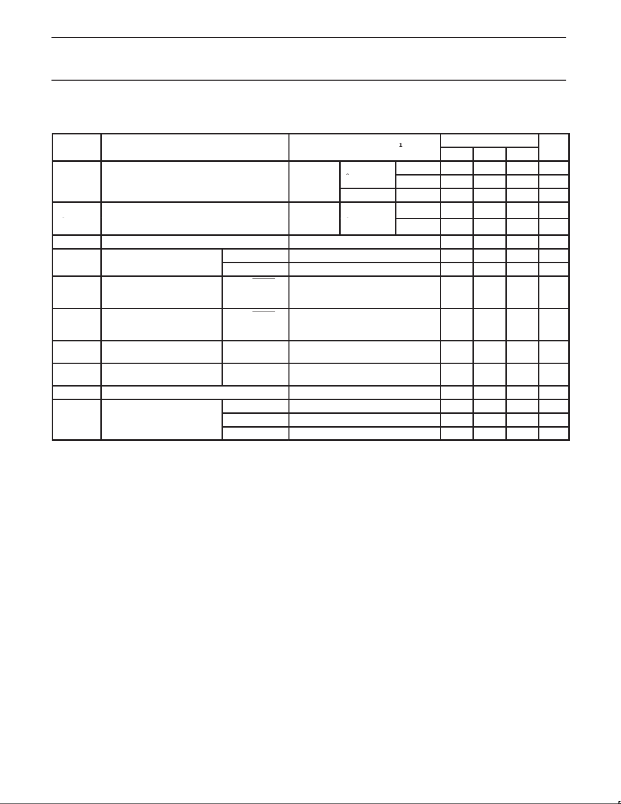
INPUT AND OUTPUT LOADING AND FAN OUT TABLE
PINS DESCRIPTION 74F (U.L.) HIGH/LOW LOAD VALUE HIGH/LOW
A0 – A7, B0 – B7 A, B inputs 3.5/0.1 16 70µA/70µA
CPAB, CPBA A–to–B, B–to–A clock inputs 1.0/0.033 20µA/20µA
SAB, SBA A–to–B, B–to–A select inputs 1.0/0.033 20µA/20µA
OEAB, OEBA A–to–B, B–to–A output enable inputs 1.0/0.033 20µA/20µA
A0 – A7, B0 – B7 A, B outputs for N74F651, N74F652 750/106.7 15mA/64mA
A0 – A7, B0 – B7 A, B outputs for N74F651A, N74F652A 750/80 15mA/48mA
A0 – A7, B0 – B7 A, B outputs for I74F652A 750/60 15mA/36mA
Note to input and output loading and fan out table
1. One (1.0) FAST unit load is defined as: 20µA in the high state and 0.6mA in the low state.
1999 Jun 23 853–1 126 21852
2
Page 3
Philips Semiconductors Product specification
74F651A/74F652ATransceivers/registers
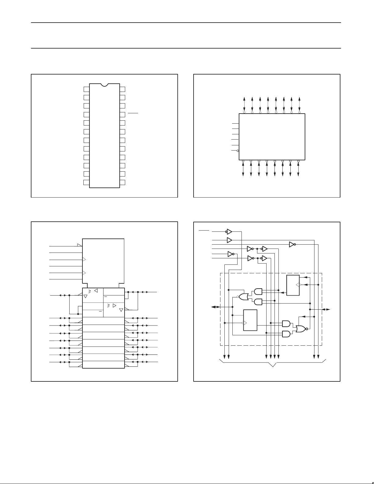
PIN CONFIGURATION
1
CPAB
2
SAB
3
OEAB
4
A0
5
A1
6
A2
7
A3
A4
8
A5
9
A6
10
A7
11
GND
IEC/IEEE SYMBOL
21
3
23
22
1
2
4
5
6
7
8
9
10
11
EN1 [BA]
EN1 [AB]
G3
G5
C6
G7
1
6D
74F651A
74F651A
1
7
1
7
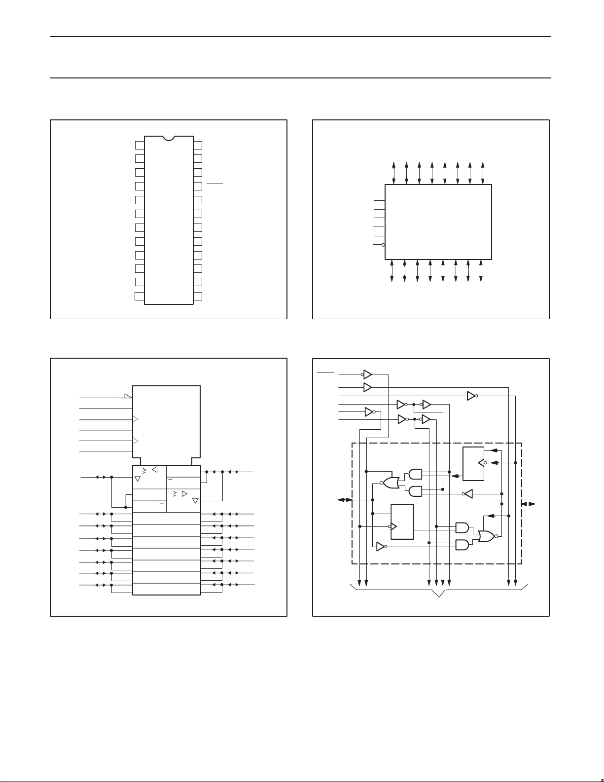
LOGIC SYMBOL
74F651A
24
V
23
22
21
20
19
18
17
16
15
14
1312
SF00401
CC
CPBA
SBA
OEBA
B0
B1
B2
B3
B4
B5
B6
B7
= Pin 24
V
CC
GND = Pin 12
4567891011
A0 A1 A2 A3 A4 A5 A6 A7
CPAB
1
SAB
2
OEAB
3
CPBA
23
SBA
22
OEBA
21
B0 B1 B2 B3 B4 B5 B6 B7
20 19 18 17 16 15 14 13
SF00402
LOGIC DIAGRAM
21
OEBA
3
OEAB
23
CPBA
22
SBA
1
CPAB
2
SAB
I of 8 channels
5
4D
1
5
1
2
20
4
A0
19
18
17
16
15
14
13
1D
C1
74F651A
1D
C1
20
B0
1999 Jun 23
SF00403
3
VCC = Pin 24
GND = Pin 12
to 7 other channels
SF00404
Page 4
Philips Semiconductors Product specification
74F651A/74F652ATransceivers/registers
PIN CONFIGURATION
1
CPAB
2
SAB
3
OEAB
4
A0
5
A1
6
A2
7
A3
A4
8
A5
9
A6
10
A7
11
GND
IEC/IEEE SYMBOL
21
3
23
22
1
2
4
5
6
7
8
9
10
11
EN1 [BA]
EN1 [AB]
G3
G5
C6
G7
1
6D
74F652A
74F652A
1
7
1
7
LOGIC SYMBOL
74F652A
24
V
23
22
21
20
19
18
17
16
15
14
1312
SF00405
CC
CPBA
SBA
OEBA
B0
B1
B2
B3
B4
B5
B6
B7
= Pin 24
V
CC
GND = Pin 12
4567891011
A0 A1 A2 A3 A4 A5 A6 A7
CPAB
1
SAB
2
OEAB
3
CPBA
23
SBA
22
OEBA
21
B0 B1 B2 B3 B4 B5 B6 B7
20 19 18 17 16 15 14 13
SF00406
LOGIC DIAGRAM
21
OEBA
3
OEAB
23
CPBA
22
SBA
1
CPAB
2
SAB
I of 8 channels
5
4D
1
5
1
2
20
4
A0
19
18
17
16
15
14
13
74F652A
1D
C1
20
1D
C1
B0
1999 Jun 23
SF00407
to 7 other channels
SF00408
4
Page 5
Philips Semiconductors Product specification
74F651A/74F652ATransceivers/registers
The following examples demonstrate the four fundamental
bus-management functions that can be performed with the 74F651A
transferred through the device in real time. The output enable pins
determine the direction of the data flow.
and 74F652A. The select pins determine whether data is stored or
BUS MANAGEMENT FUNCTIONS
REAL TIME BUS TRANSFER
BUS A
OEAB OEBA CPAB CPBA SAB SBA
L LX XXL HHXXLX XH↑ XXX
BUS B TO BUS A
BUS B
REAL TIME BUS TRANSFER
BUS A TO BUS B
BUS A BUS A
OEAB OEBA
CPAB CPBA SAB SBA
STORAGE FROM
A, B, OR A AND B
OEAB OEBA
LXX↑ XX
LH↑↑XX
CPAB CPBA SAB SBA OEAB OEBA CPAB CPBA SAB SBA
TRANSFER STORED DATA
TO A AND/OR B
BUS A BUS BBUS BBUS B
H L H or L H or L H H
SF00409
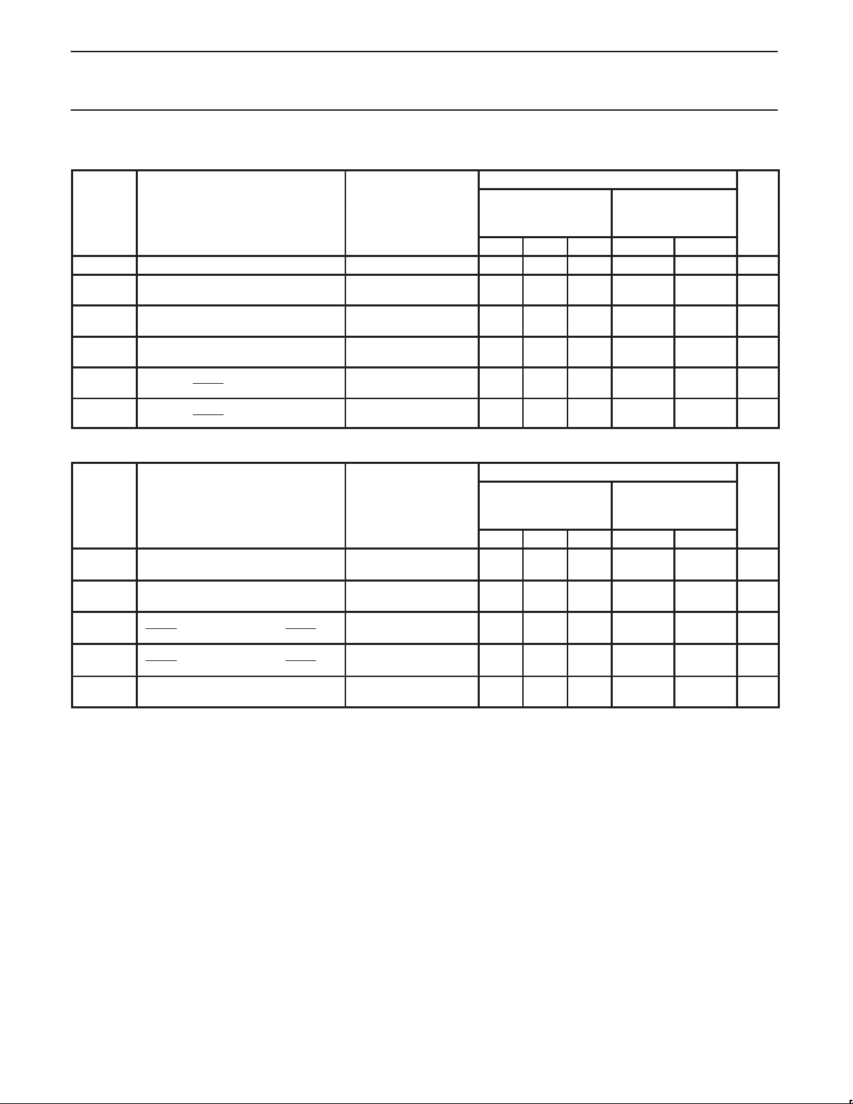
FUNCTION TABLE
INPUTS DATA I/O OPERATING MODE
OEAB OEBA CPAB CPBA SAB SBA An Bn 74F651A 74F652A
L H H or L H or L X X Input Input Isolation Isolation
L H ↑ ↑ X X Input Input Store A and B data Store A and B data
X H ↑ H or L X X Input Unspecified* Store A, hold B Store A hold B
H H ↑ ↑ L X Input Output Store A in both registers Store A in both registers
L X H or L ↑ X X Unspecified* Input Hold A, store B Hold A, store B
L L ↑ ↑ X L Output Input Store B in both registers Store B in both registers
L L X X X L Output Input Real time B data to A bus Real time B data to A bus
L L X H or L X H Output Input Stored B data to A bus Stored B data to A bus
H H X X L X Input Output Real time A data to B bus Real time A data to B bus
H H H or L X H X Input Output Stored A data to B bus Stored A data to B bus
H L H or L H or L H H Output Output Stored A data to B bus Stored A data to B bus
H L H or L H or L H H Output Output Stored B data to A bus Stored B data to A bus
Notes to function table
1. H = High-voltage level
2. L = Low-voltage level
3. * = The data output function may be enabled or disabled by various signals at the OEBA
always enabled, i.e., data at the bus pins will be stored on every low-to-high transition of the clock.
4. ↑ = Low-to-high clock transition
5. X = Don’t care
and OEAB inputs. Data input functions are
1999 Jun 23
5
Page 6
Philips Semiconductors Product specification
T
Operating free air temperature range
SYMBOL
PARAMETER
UNIT
IOLLow-level output current
T
Operating free air temperature range
74F651A/74F652ATransceivers/registers
ABSOLUTE MAXIMUM RATINGS
Operation beyond the limit set forth in this table may impair the useful life of the device.
Unless otherwise noted these limits are over the operating free air temperature range.
SYMBOL
V
V
I
IN
V
I
OUT
T
CC
IN
OUT
amb
stg
Supply voltage –0.5 to +7.0 V
Input voltage –0.5 to +7.0 V
Input current –30 to +5 mA
Voltage applied to output in high output state –0.5 to V
Current applied to output in low output state 72 mA
p
p
Storage temperature range –65 to +150 °C
RECOMMENDED OPERATING CONDITIONS
V
V
V
I
I
CC
IH
IL
Ik
OH
amb
Supply voltage 4.5 5.0 5.5 V
High-level input voltage 2.0 V
Low-level input voltage 0.8 V
Input clamp current –18 mA
High-level output current –15 mA
p
p
p
PARAMETER RATING UNIT
CC
V
Commercial range 0 to +70 °C
Industrial range –40 to +85 °C
LIMITS
MIN NOM MAX
Commercial range 48 mA
Industrial range (74F652A only) 36 mA
Commercial range 0 +70 °C
Industrial range (74F652A only) –40 +85 °C
1999 Jun 23
6
Page 7
Philips Semiconductors Product specification
SYMBOL
PARAMETER
TEST CONDITIONS
1
UNIT
V
CC
MIN
I
3mA
V
MIN
VOLLow-level output voltage
V
MAX
I
MAX
I
74F651A/74F652ATransceivers/registers
DC ELECTRICAL CHARACTERISTICS
Over recommended operating free-air temperature range unless otherwise noted.
LIMITS
MIN TYP2MAX
=
=
,
= –
V
V
OH
High-level output voltage
= MAX,
IL
=
IH
OH
IOH = –15mA ±10%V
VCC = MIN,
=
p
V
IK
I
Input clamp voltage VCC = MIN, II = I
Input current at maximum input
voltage
others VCC = 0.0V, VI = 7.0V 100 µA
A0–A7, B0–B7 VCC = 5.5V, VI = 5.5V 1 mA
IL
V
IH
= MIN
,
=
OL
IK
±10%V
±5%V
±10%V
±5%V
OEAB, OEBA,
I
IH
High-level input current
CPAB, CPBA,
SAB, SBA
VCC = MAX, VI = 2.7V 20 µA
OEAB, OEBA,
I
IL
I
OZH
I
OZL
I
O
I
CC
Low-level input current
+ I
+ I
Off-state output current,
IH
high-level voltage applied
Off–state output current,
IL
low–level voltage applied
Output current
3
Supply current (total)
CPAB, CPBA,
VCC = MAX, VI = 0.5V –20 µA
SAB, SBA
A0–A7, B0–B7 VCC = MAX, V
= 2.7V 70 µA
O
A0–A7, B0–B7 VCC = MAX, VO = 0.5V –70 µA
VCC = MAX, V0 = 2.25V –60 –160 mA
I
CCH
I
CCL
I
CCZ
VCC = MAX 105 145 mA
VCC = MAX 115 165 mA
VCC = MAX 115 160 mA
NOTES:
1. For conditions shown as MIN or MAX, use the appropriate value specified under recommended operating conditions for the applicable type.
2. All typical values are at VCC = 5V, T
is tested under conditions that produce current approximately one half of the true short–circuit output current (IOS).
3. I
O
amb
= 25°C.
2.4 V
CC
2.7 3.3 V
CC
2.0 V
CC
CC
CC
0.42 0.55 V
–0.73 –1.2 V
0.55 V
1999 Jun 23
7
Page 8
Philips Semiconductors Product specification
74F651A/74F652ATransceivers/registers
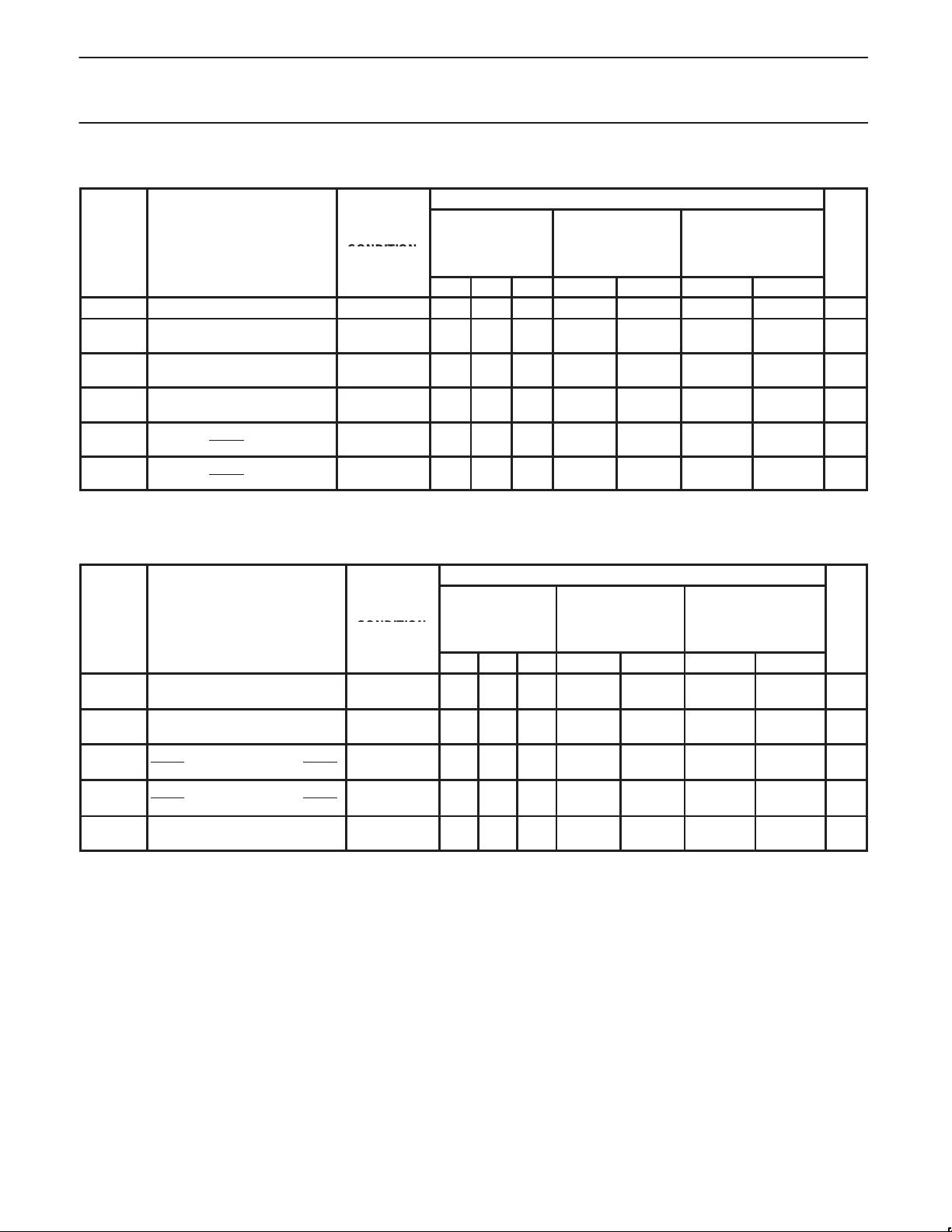
AC ELECTRICAL CHARACTERISTICS FOR 74F651A
LIMITS
T
= +25°C T
amb
SYMBOL PARAMETER TEST CONDITION VCC = +5.0V VCC = +5.0V ± 10% UNIT
CL = 50pF, RL = 500Ω CL = 50pF, RL = 500Ω
MIN TYP MAX MIN MAX
f
max
t
PLH
t
PHL
t
PLH
t
PHL
t
PLH
t
PHL
t
PZH
t
PZL
t
PHZ
t
PLZ
Maximum clock frequency Waveform 1 155 175 140 ns
Propagation delay
CPAB or CPBA to An or Bn
Propagation delay
An or Bn to Bn or An
Propagation delay
SAB or SBA to An or Bn
Output enable time
OEAB or OEBA to An or Bn
Output disable time
OEAB or OEBA to An or Bn
Waveform 1
Waveform 2, 3
Waveform 2, 3
Waveform 7, 8
Waveform 7, 8
4.5
5.5
2.5
4.0
4.0
5.0
3.0
3.5
1.5
2.5
7.0
7.5
4.5
6.5
7.0
7.0
5.0
6.0
4.0
6.0
10.0
10.5
7.5
9.0
10.0
10.0
8.0
8.5
7.0
8.5
= 0°C to +70°C
amb
4.0
5.0
2.0
4.0
3.5
4.5
2.5
3.0
1.0
2.0
11.0
11.0
8.5
10.0
12.0
10.0
8.5
9.0
7.5
9.0
ns
ns
ns
ns
ns
AC SETUP REQUIREMENTS FOR 74F651A
LIMITS
T
= +25°C T
amb
SYMBOL PARAMETER TEST CONDITION VCC = +5.0V VCC = +5.0V ± 10% UNIT
CL = 50pF, RL = 500Ω C
MIN TYP MAX MIN MAX
t
(H)
su
t
(L)
su
t
(H)
h
t
(L)
h
t
(H)
su
t
(L)
su
t
(H)
h
t
(L)
h
t
(H)
w
t
(L)
w
Setup time, high or low
An or Bn to CPAB or CPBA
Hold time, high or low
An or Bn to CPAB or CPBA
Setup time, high or low
OEBA to OEAB or OEAB to OEBA
Hold time, high or low
OEBA to OEAB or OEAB to OEBA
Pulse width, high or low
CPAB or CPBA
Waveform 4
Waveform 4
Waveform 5, 6
Waveform 5, 6
Waveform 1
3.5
4.0
0
0
5.0
5.0
0
0
4.5
3.5
Note to AC setup requirements for 74F651A:
1. Setup time is to protect against surge current caused by enabling 16 outputs (48mA per output) simultaneously.
= 0°C to +70°C
amb
= 50pF, RL = 500Ω
L
4.0
4.5
0
0
5.0
5.0
0
0
4.5
4.0
ns
ns
ns
ns
ns
1999 Jun 23
8
Page 9
Philips Semiconductors Product specification
SYMBOL
PARAMETER
UNIT
SYMBOL
PARAMETER
UNIT
74F651A/74F652ATransceivers/registers
AC ELECTRICAL CHARACTERISTICS FOR 74F652A
LIMITS
T
f
max
t
PLH
t
PHL
t
PLH
t
PHL
t
PLH
t
PHL
t
PZH
t
PZL
t
PHZ
t
PLZ
= +25°C T
TEST
CONDITION
amb
VCC = +5.0V VCC = +5.0V ± 10% VCC = +5.0V ± 10%
CL = 50pF,
RL = 500Ω
MIN TYP MAX MIN MAX MIN MAX
Maximum clock frequency Waveform 1 155 175 140 140 ns
Propagation delay
CPAB or CPBA to An or Bn
Propagation delay
An or Bn to Bn or An
Propagation delay
SAB or SBA to An or Bn
Output enable time1
OEAB or OEBA to An or Bn
Output disable time
OEAB or OEBA to An or Bn
Waveform 1
Waveform 1
Waveform 2, 3
Waveform 7, 8
Waveform 7, 8
5.0
5.0
4.0
3.0
4.5
4.0
3.0
3.5
1.5
2.5
7.5
7.0
6.0
5.0
7.0
8.0
5.0
6.0
4.0
6.0
10.0
10.0
9.0
8.0
10.0
10.0
8.0
8.5
7.0
8.5
= 0°C to +70°C T
amb
CL = 50pF,
RL = 500Ω
4.5
4.5
3.5
2.5
4.0
4.0
2.5
3.0
1.0
2.0
11.5
10.5
10.0
8.5
11.0
11.5
8.5
9.0
7.5
9.0
= –40°C to +85°C
amb
CL = 50pF,
RL = 500Ω
4.5
4.5
3.5
2.5
4.0
4.0
2.5
3.0
1.0
2.0
11.5
10.5
10.0
8.5
11.0
11.5
8.5
9.0
7.5
9.0
ns
ns
ns
ns
ns
AC SETUP REQUIREMENTS FOR 74F652A
LIMITS
T
= +25°C T
TEST
CONDITION
amb
VCC = +5.0V VCC = +5.0V ± 10% VCC = +5.0V ± 10%
CL = 50pF,
RL = 500Ω
MIN TYP MAX MIN MAX MIN MAX
t
(H)
su
t
su
t
(H)
h
t
(L)
h
t
su
t
su
t
(H)
h
t
(L)
h
t
(H)
w
t
(L)
w
Setup time, high or low
(L)
An or Bn to CPAB or CPBA
Hold time, high or low
An or Bn to CPAB or CPBA
(H)
Setup time, high or low
(L)
OEBA to OEAB or OEAB to OEBA
Hold time, high or low
OEBA to OEAB or OEAB to OEBA
Pulse width, high or low
CPAB or CPBA
Waveform 4
Waveform 4
Waveform 5, 6
Waveform 5, 6
Waveform 1
3.5
4.0
0
0
5.0
5.0
0
0
4.0
3.5
Note to AC setup requirements for 74F652A
1. Setup time is to protect against surge current caused by enabling 16 outputs (48mA per output) simultaneously.
= 0°C to +70°C T
amb
CL = 50pF,
RL = 500Ω
4.0
4.5
0
0
5.0
5.0
0
0
4.5
4.0
= –40°C to +85°C
amb
CL = 50pF,
RL = 500Ω
4.0
4.5
0
0
5.0
5.0
0
0
4.5
4.0
ns
ns
ns
ns
ns
1999 Jun 23
9
Page 10
Philips Semiconductors Product specification
74F651A/74F652ATransceivers/registers
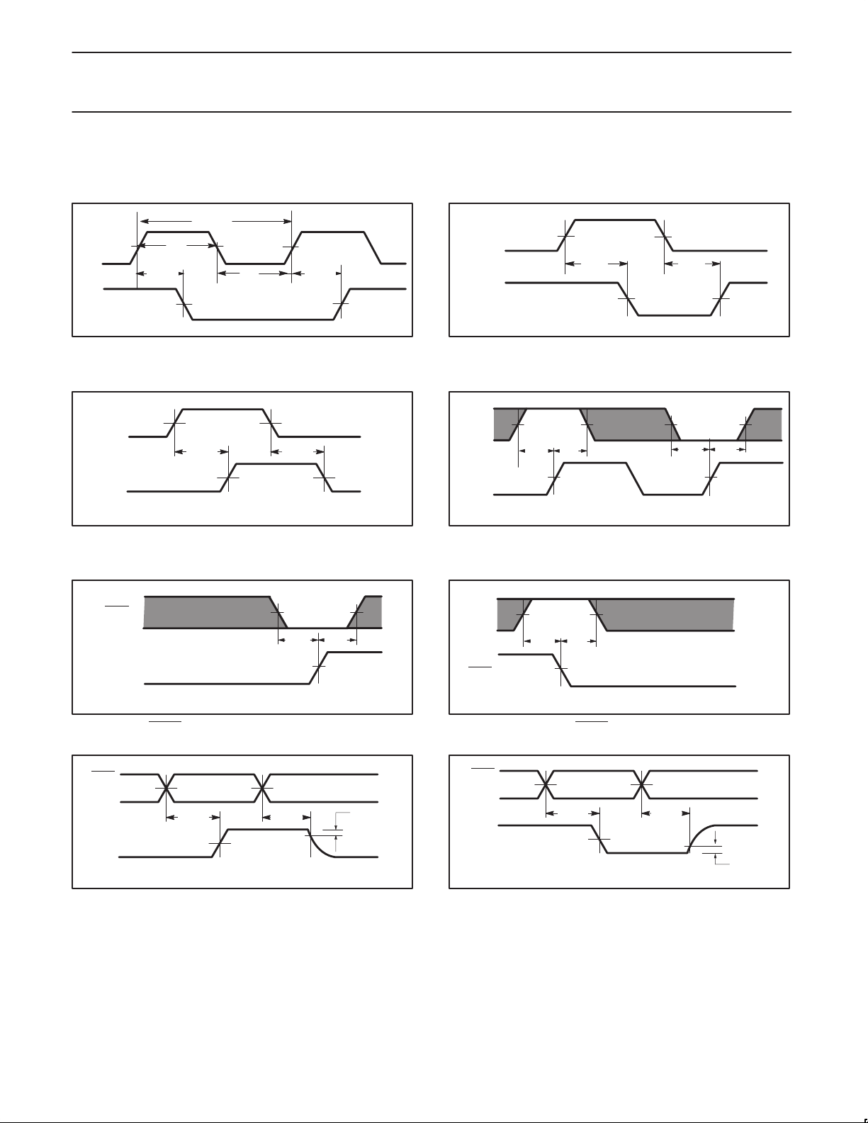
AC WAVEFORMS
For all waveforms, VM = 1.5V.
The shaded areas indicate when the input is permitted to change for predictable output performance.
1/f
CPBA
or
CPAB
An or Bn
V
M
t
PHL
tw(H)
max
V
M
tw(L)
V
M
V
M
t
PLH
V
M
SF00394
Waveform 1. Propagation delay for clock input to output, clock
pulse width, and maximum clock frequency
An or Bn
Bn or An
V
M
t
PHL
V
M
V
M
SBA or SAB
t
PLH
V
M
An or Bn
SF00395
Waveform 2. Propagation delay for An to Bn or Bn to An and
SAB or SBA to An or Bn
t
PHL
V
M
SBA or SAB
An or Bn
SF00396
An or Bn
Bn or An
V
t
PLH
M
V
M
V
M
Waveform 3. Propagation delay for An to Bn or Bn to An and
SAB or SBA to An or Bn
OEBA
OEAB
V
M
tsu(L) th(L)
V
M
V
M
SF00410
Waveform 5. OEBA to OEAB setup time and hold times
OEBA
OEAB
An or Bn
V
t
PZH
M
V
V
M
t
PHZ
M
VOH -0.3V
0V
SF00412
Waveform 7. 3-State output enable time to high level and
output disable time from high level
An or Bn
CPBA
CPAB
or
V
M
(H) th(H)
t
su
V
M
V
M
V
tsu(L) th(L)
V
M
V
M
M
Waveform 4. Data setup time and hold times
OEAB
OEBA
V
tsu(H) th(H)
V
M
V
M
M
SF00411
Waveform 6. OEAB to OEBA setup time and hold times
OEBA
OEAB
An or Bn
V
t
PZL
M
V
V
M
t
PLZ
M
VOL +0.3V
SF00413
Waveform 8. 3-State output enable time to low level and
output disable time from low level
SF00397
1999 Jun 23
10
Page 11
Philips Semiconductors Product specification
74F651A/74F652ATransceivers/registers
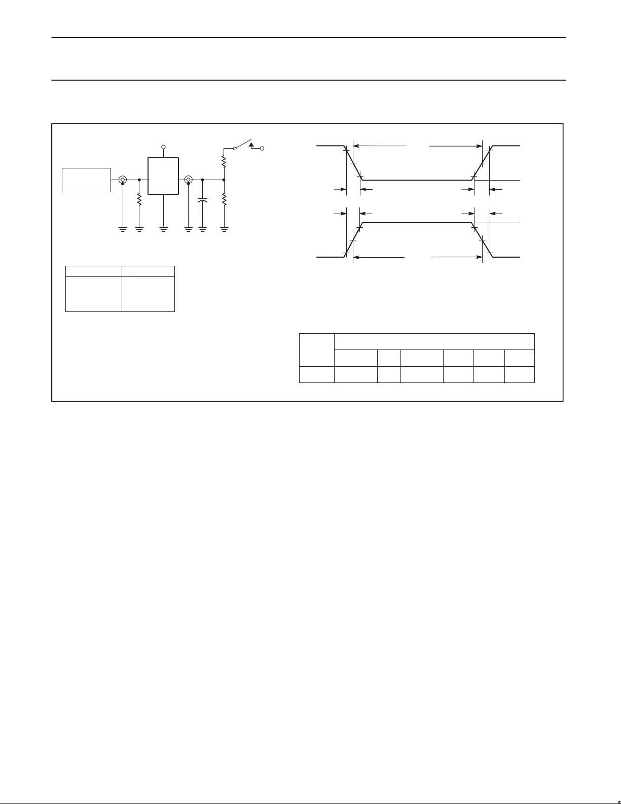
TEST CIRCUIT AND WAVEFORMS
V
CC
PULSE
GENERATOR
V
IN
R
T
D.U.T.
V
OUT
Test Circuit for Open Collector Outputs
SWITCH POSITION
TEST SWITCH
t
t
PLZ
PZL
closed
closed
All other open
7.0V
R
L
C
R
L
L
NEGATIVE
PULSE
POSITIVE
PULSE
90%
10%
V
M
10%
t
THL (tf
t
TLH (tr
90%
V
M
Input Pulse Definition
t
w
V
M
10%
)
)
t
)
TLH (tr
t
)
THL (tf
90%
V
M
t
w
90%
10%
AMP (V)
0V
AMP (V)
0V
DEFINITIONS:
= Load resistor;
R
L
see AC electrical characteristics for value.
C
= Load capacitance includes jig and probe capacitance;
L
see AC electrical characteristics for value.
R
= Termination resistance should be equal to Z
T
pulse generators.
OUT
of
family
74F
INPUT PULSE REQUIREMENTS
V
amplitude
3.0V
M
1.5V
rep. rate
1MHz 500ns
t
w
t
TLHtTHL
2.5ns 2.5ns
SF00128
1999 Jun 23
11
Page 12
Philips Semiconductors Product specification
74F651A/74F652ATransceivers/registers
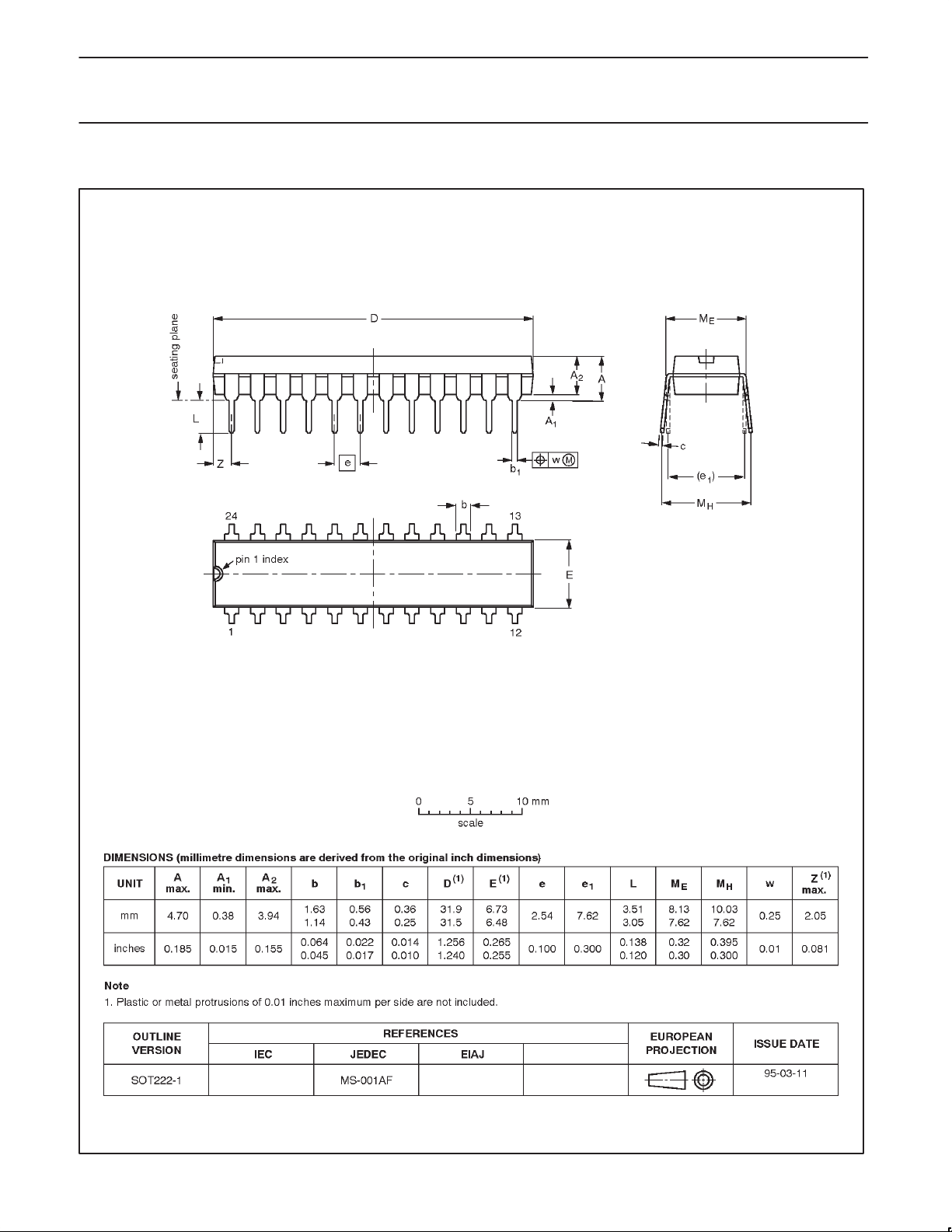
DIP24: plastic dual in-line package; 24 leads (300 mil) SOT222-1
1999 Jun 23
12
Page 13
Philips Semiconductors Product specification
74F651A/74F652ATransceivers/registers
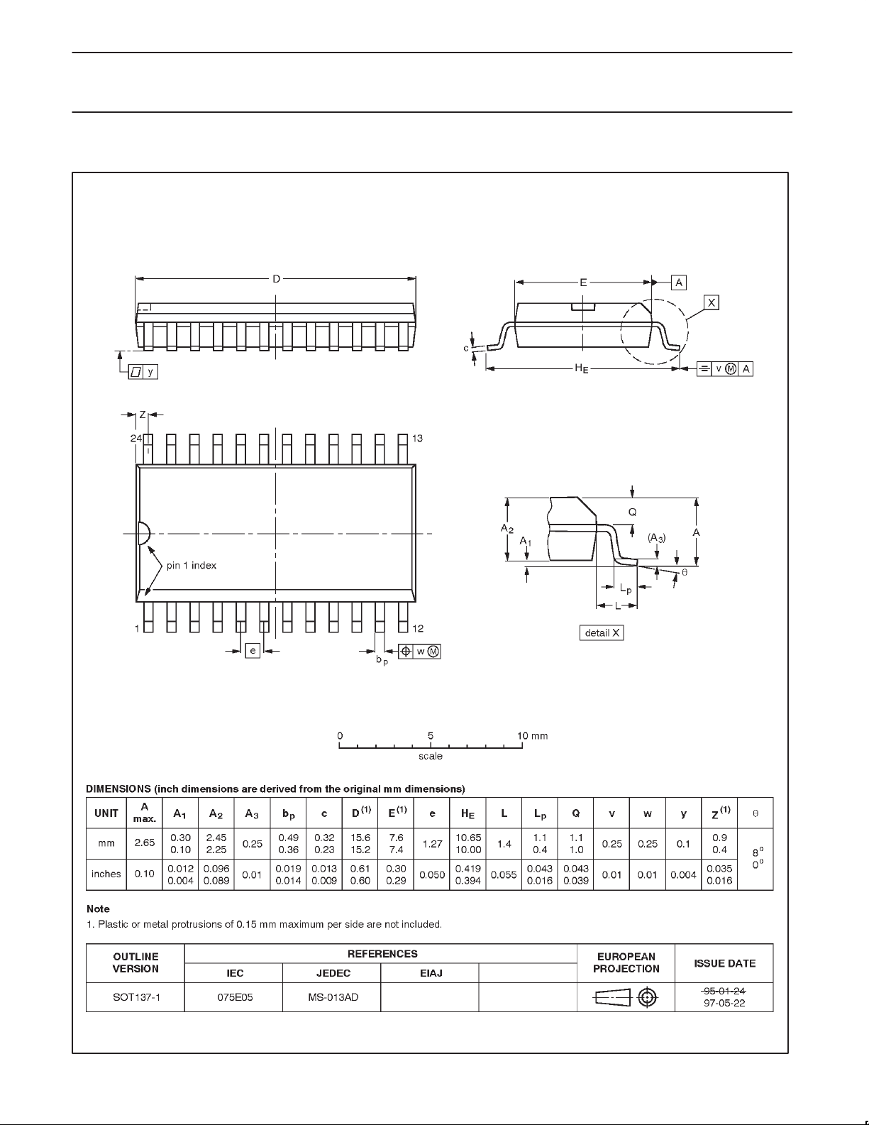
SO24: plastic small outline package; 24 leads; body width 7.5 mm SOT137-1
1999 Jun 23
13
Page 14
Philips Semiconductors Product specification
74F651A/74F652ATransceivers/registers
Data sheet status
Data sheet
status
Objective
specification
Preliminary
specification
Product
specification
Product
status
Development
Qualification
Production
Definition
This data sheet contains the design target or goal specifications for product development.
Specification may change in any manner without notice.
This data sheet contains preliminary data, and supplementary data will be published at a later date.
Philips Semiconductors reserves the right to make changes at any time without notice in order to
improve design and supply the best possible product.
This data sheet contains final specifications. Philips Semiconductors reserves the right to make
changes at any time without notice in order to improve design and supply the best possible product.
[1]
[1] Please consult the most recently issued datasheet before initiating or completing a design.
Definitions
Short-form specification — The data in a short-form specification is extracted from a full data sheet with the same type number and title. For
detailed information see the relevant data sheet or data handbook.
Limiting values definition — Limiting values given are in accordance with the Absolute Maximum Rating System (IEC 134). Stress above one
or more of the limiting values may cause permanent damage to the device. These are stress ratings only and operation of the device at these or
at any other conditions above those given in the Characteristics sections of the specification is not implied. Exposure to limiting values for extended
periods may affect device reliability.
Application information — Applications that are described herein for any of these products are for illustrative purposes only. Philips
Semiconductors make no representation or warranty that such applications will be suitable for the specified use without further testing or
modification.
Disclaimers
Life support — These products are not designed for use in life support appliances, devices or systems where malfunction of these products can
reasonably be expected to result in personal injury . Philips Semiconductors customers using or selling these products for use in such applications
do so at their own risk and agree to fully indemnify Philips Semiconductors for any damages resulting from such application.
Right to make changes — Philips Semiconductors reserves the right to make changes, without notice, in the products, including circuits, standard
cells, and/or software, described or contained herein in order to improve design and/or performance. Philips Semiconductors assumes no
responsibility or liability for the use of any of these products, conveys no license or title under any patent, copyright, or mask work right to these
products, and makes no representations or warranties that these products are free from patent, copyright, or mask work right infringement, unless
otherwise specified.
Philips Semiconductors
811 East Arques Avenue
P.O. Box 3409
Sunnyvale, California 94088–3409
Telephone 800-234-7381
Copyright Philips Electronics North America Corporation 1999
All rights reserved. Printed in U.S.A.
Date of release: 06-99
Document order number: 9397 750 06142
1999 Jun 23
14
 Loading...