

Page 1
74F641/74F642*
Transceivers
Product specification
Supersedes data of 1989 Nov 27
IC15 Data Handbook
1999 Jan 08
INTEGRATED CIRCUITS
* Discontinued part. Please see the Discontinued Product List.
Page 2
Philips Semiconductors Product specification
74F641/74F642*Transceivers
74F641 Octal Bus Transceiver with Common Output Enable, Non-Inverting (Open Collector)
74F642 Octal Bus Transceiver with Common Output Enable, Inverting (Open Collector)
2
1999 Jan 08 853–0382 20616
* Discontinued part. Please see the Discontinued Products List.
FEA TURES
•High-impedance NPN base inputs for reduced loading
(20µA in High and Low states)
•Octal bidirectional bus interface
•Common Output Enable for both Transmit and Receive modes
•Open collector outputs sink 64mA
•—74F641, non-inverting
—74F642, inverting
ORDERING INFORMATION
DESCRIPTION
COMMERCIAL RANGE
VCC = 5V ±10%,
T
amb
= 0°C to +70°C
PKG DWG #
20-pin plastic DIP N74F641N SOT146-1
20-pin plastic SOL N74F641D SOT163-1
TYPE
TYPICAL
PROPAGATION
DELA Y
TYPICAL SUPPL Y CURRENT
(TOT AL)
74F641 8.0ns 69mA
74F642 8.5ns 52mA
INPUT AND OUTPUT LOADING AND FAN-OUT TABLE
PINS DESCRIPTION
74F(U.L.)
HIGH/LOW
LOAD VALUE
HIGH/LOW
A0 - A7, B0 - B7 Data inputs 1.0/0.033 20µA/20µA
T/R Transmit/Receive input 2.0/0.067 40µA/40µA
OE Output Enable inputs 2.0/0.067 40µA/40µA
A0 - A7 Data outputs OC/40 OC/24mA
B0 - B7 Data outputs OC/106.7 OC/64mA
NOTE: One (1.0) FAST unit load is defined as: 20µA in the High state and 0.6mA in the Low state. OC = Open Collector.
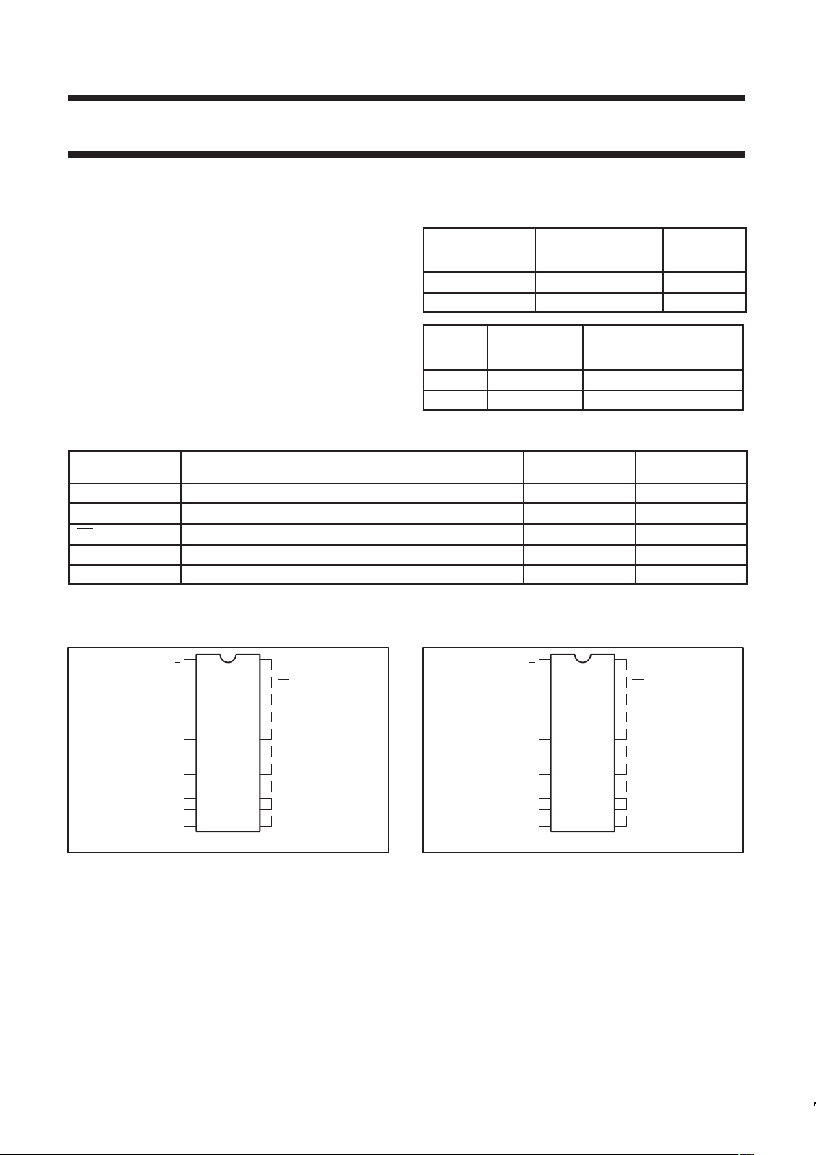
PIN CONFIGURATION – 74F641
SF00198
1
2
3
4
5
6
7
8
9
10 11
12
13
14
15
16
17
18
19
20
T/R
A0
A1
A2
A3
A4
A5
A6
A7
GND
V
CC
OE
B0
B1
B2
B3
B4
B6
B5
B7
PIN CONFIGURATION – 74F642
SF00198
1
2
3
4
5
6
7
8
9
10 11
12
13
14
15
16
17
18
19
20
T/R
A0
A1
A2
A3
A4
A5
A6
A7
GND
V
CC
OE
B0
B1
B2
B3
B4
B6
B5
B7
Page 3
Philips Semiconductors Product specification
74F641/74F642*Transceivers
1999 Jan 08
3
* Discontinued part. Please see the Discontinued Products List.
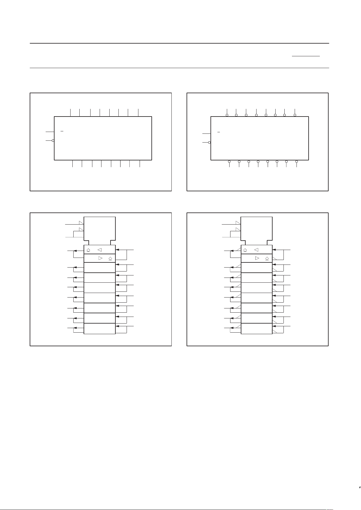
LOGIC SYMBOL – 74F641
B0 B1 B2 B3
19
1
T/R
OE
SF01154
VCC= Pin 20
GND = Pin 10
B4 B5 B6 B7
89
A2 A3
456
A4 A5 A67A7
23
A0 A1
18 17 16 15 14 13 12 11
LOGIC SYMBOL – 74F642
B0 B1 B2 B3
19
1
T/R
OE
SF01146
VCC= Pin 20
GND = Pin 10
B4 B5 B6 B7
89
A2 A3
456
A4 A5 A67A7
23
A0 A1
18 17 16 15 14 13 12 11
LOGIC SYMBOL (IEEE/IEC) – 74F641
SF01147
19
18
G3
3EN1
3EN2
1
17
16
15
14
13
12
11
2
3
4
5
6
7
8
9
2
1
LOGIC SYMBOL (IEEE/IEC) – 74F642
SF01148
19
18
G3
3EN1
3EN2
1
17
16
15
14
13
12
11
2
3
4
5
6
7
8
9
2
1
Page 4

Philips Semiconductors Product specification
74F641/74F642*Transceivers
1999 Jan 08
4
* Discontinued part. Please see the Discontinued Products List.
LOGIC DIAGRAM – 74F641
VCC= Pin 20
GND = Pin 10
SF01149
T/R
2
3
4
18
17
16
15
14
13
12
B0
B1
B4
B5
B6
B7
OE
A1
A4
A5
A6
A7
B2
B3
A3
A2
5
6
7
8
A0
11
9
19
1
LOGIC DIAGRAM – 74F642
VCC= Pin 20
GND = Pin 10
SF01150
T/R
2
3
4
18
17
16
15
14
13
12
B0
B1
B4
B5
B6
B7
OE
A1
A4
A5
A6
A7
B2
B3
A3
A2
5
6
7
8
A0
11
9
19
1
FUNCTION TABLE – 74F641
INPUTS INPUTS/OUTPUTS
OE T/R An Bn
L L A=B INPUTS
H H INPUTS B=A
H X OFF OFF
H = High voltage level
L = Low voltage level
X = Don’t care
OFF= High if pull-up resistor is connected to open collector output
FUNCTION TABLE – 74F642
INPUTS INPUTS/OUTPUTS
OE T/R An Bn
L L A=B INPUTS
H H INPUTS B=A
H X OFF OFF
H = High voltage level
L = Low voltage level
X = Don’t care
OFF= High if pull-up resistor is connected to open collector output
Page 5

Philips Semiconductors Product specification
74F641/74F642*Transceivers
1999 Jan 08
5
* Discontinued part. Please see the Discontinued Products List.
ABSOLUTE MAXIMUM RATINGS
(Operation beyond the limits set forth in this table may impair the useful life of the device.
Unless otherwise noted these limits are over the operating free-air temperature range.)
SYMBOL
PARAMETER RATING UNIT
V
CC
Supply voltage –0.5 to +7.0 V
V
IN
Input voltage –0.5 to +7.0 V
I
IN
Input current –30 to +5 mA
V
OUT
Voltage applied to output in High output state –0.5 to +V
CC
V
pp
p
p
A0–A7 48 mA
I
OUT
Current a lied to out ut in Low out ut state
B0–B7 128 mA
T
amb
Operating free-air temperature range 0 to +70 °C
T
stg
Storage temperature range –65 to +150 °C
RECOMMENDED OPERATING CONDITIONS
LIMITS
SYMBOL
PARAMETER
MIN NOM MAX
UNIT
V
CC
Supply voltage 4.5 5.0 5.5 V
V
IH
High-level input voltage 2.0 V
V
IL
Low-level input voltage 0.8 V
I
IK
Input clamp current –18 mA
I
OH
High-level output current 4.5 V
p
A0–A7 24 mA
IOLLow-level out ut current
B0–B7 64 mA
T
amb
Operating free-air temperature range 0 70 °C
DC ELECTRICAL CHARACTERISTICS
(Over recommended operating free-air temperature range unless otherwise noted.)
LIMITS
SYMBOL PARAMETER TEST CONDITIONS
NO TAG
MIN
TYP
NO TAG
MAX
UNIT
I
OH
High-level output current
VCC = MIN, VIL = MAX,
V
IH
= MIN, V
OH
= MAX
250 µA
±10%V
CC
0.35 0.50 V
p
A0–A7
VCC = MIN,
I
OL
=
24mA
±5%V
CC
0.35 0.50 V
VOLLow-level out ut voltage
V
IL
=
MAX
,
V
IH
= MIN,
IOL = 48mA ±10%V
CC
0.38 0.55 V
B0–B7
IH
,
IOL = 64mA ±5%V
CC
0.42 0.55 V
V
IK
Input clamp voltage VCC = MIN, II = I
IK
–0.73 –1.2 V
Input current at maximum
T/R, OE VCC = 0.0V, VI = 7.0V 100 µA
I
I
input voltage
An, Bn VCC = 5.5V, VI = 5.5V 1 mA
p
T/R, OE
40 µA
IIHHigh-level in ut current
An, Bn
V
CC
=
MAX, V
I
= 2.
7V
20 µA
p
T/R, OE
–40 µA
IILLow-level in ut current
An, Bn
V
CC
=
MAX, V
I
= 0.
5V
–20 µA
I
CCH
An=T/R=4.5, OE=GND 60 90 mA
Supply current
74F641
I
CCL
T/R=4.5V, An=OE=GND 78 120 mA
I
CC
y
(total)
I
CCH
V
CC
=
MAX
An=T/R=OE=4.5V 37 55 mA
74F642
I
CCL
An=T/R=4.5V, OE=GND 67 98 mA
NOTES:
1. For conditions shown as MIN or MAX, use the appropriate value specified under recommended operating conditions for the applicable type.
2. All typical values are at V
CC
= 5V, T
amb
= 25°C.
Page 6

Philips Semiconductors Product specification
74F641/74F642*Transceivers
1999 Jan 08
6
* Discontinued part. Please see the Discontinued Products List.
AC ELECTRICAL CHARACTERISTICS – 74F641
LIMITS
SYMBOL PARAMETER
TEST
CONDITION
VCC = +5V
T
amb
= +25°C
C
L
= 50pF, RL = 500Ω
VCC = +5V ± 10%
T
amb
= 0°C to +70°C
C
L
= 50pF, RL = 500Ω
UNIT
MIN TYP MAX MIN MAX
t
PLH
t
PHL
Propagation delay
An to Bn
Waveform
NO TAG
6.5
4.0
8.5
6.0
11.5
9.5
6.5
4.0
12.5
11.0
ns
t
PLH
t
PHL
Propagation delay
Bn to An
Waveform
NO TAG
6.0
3.5
8.0
5.5
11.5
7.5
6.0
3.5
12.0
8.0
ns
t
PLH
t
PHL
Propagation delay
OE to An
Waveform 4
7.0
5.0
10.5
7.0
12.5
9.0
7.0
5.0
13.0
10.0
ns
t
PLH
t
PHL
Propagation delay
OE to Bn
Waveform 4
8.0
3.5
9.0
7.5
12.5
9.5
8.0
5.5
13.5
10.5
ns
AC ELECTRICAL CHARACTERISTICS – 74F642
LIMITS
SYMBOL PARAMETER
TEST
CONDITION
VCC = +5V
T
amb
= +25°C
C
L
= 50pF, RL = 500Ω
VCC = +5V ± 10%
T
amb
= 0°C to +70°C
C
L
= 50pF, RL = 500Ω
UNIT
MIN TYP MAX MIN MAX
t
PLH
t
PHL
Propagation delay
An to Bn
Waveform
NO TAG
8.0
2.0
9.0
4.5
12.5
6.5
8.0
2.0
13.5
7.0
ns
t
PLH
t
PHL
Propagation delay
Bn to An
Waveform
NO TAG
7.5
1.5
8.0
4.0
12.0
6.0
7.5
1.5
12.5
6.5
ns
t
PLH
t
PHL
Propagation delay
OE to An
Waveform
NO TAG
7.5
6.0
9.0
8.0
12.0
10.5
7.5
6.0
12.5
11.0
ns
t
PLH
t
PHL
Propagation delay
OE to Bn
Waveform
NO TAG
8.0
6.0
9.0
7.0
12.5
10.5
8.0
6.0
13.0
11.0
ns
AC WAVEFORMS
For all waveforms, VM = 1.5V .
V
M
V
M
V
M
V
M
Bn or An
An or Bn
t
PLH
t
PHL
SF01131
Waveform 1. Propagation Delay for An to Bn or Bn to An
(74F642)
V
M
V
M
V
M
V
M
Bn or An
An or Bn
t
PLH
t
PHL
SF01132
Waveform 2. Propagation Delay for An to Bn or Bn to An
(74F641)
Page 7

Philips Semiconductors Product specification
74F641/74F642*Transceivers
1999 Jan 08
7
* Discontinued part. Please see the Discontinued Products List.
AC WAVEFORMS (Continued)
For all waveforms, VM = 1.5V .
V
M
V
M
V
M
V
M
An or Bn
OE
t
PLH
t
PHL
SF01151
Waveform 3. Propagation Delay for OE to An or Bn Outputs
(74F642) (Bn or An Inputs in High State)
V
M
V
M
V
M
V
M
An or Bn
OE
t
PLH
t
PHL
SF01151
Waveform 4. Propagation Delay for OE to An or Bn Outputs
(74F641) (Bn or An Inputs in Low State)
TEST CIRCUIT AND WAVEFORMS
t
w
90%
V
M
10%
90%
V
M
10%
90%
V
M
10%
90%
V
M
10%
NEGATIVE
PULSE
POSITIVE
PULSE
t
w
AMP (V)
0V
0V
t
THL (tf
)
INPUT PULSE REQUIREMENTS
rep. rate
t
w
t
TLHtTHL
1MHz 500ns
2.5ns 2.5ns
Input Pulse Definition
V
CC
family
74F
D.U.T.
PULSE
GENERATOR
R
L
C
L
R
T
V
IN
V
OUT
Test Circuit for 3-State Outputs
DEFINITIONS:
R
L
= Load resistor;
see AC electrical characteristics for value.
C
L
= Load capacitance includes jig and probe capacitance;
see AC electrical characteristics for value.
R
T
= Termination resistance should be equal to Z
OUT
of
pulse generators.
t
THL (tf
)
t
TLH (tr
)
t
TLH (tr
)
AMP (V)
amplitude
3.0V
1.5V
V
M
R
L
7.0V
SF00777
TEST SWITCH
t
PLZ
closed
t
PZL
closed
All other open
SWITCH POSITION
Page 8

Philips Semiconductors Product specification
74F641/74F642*Transceivers
1999 Jan 08
8
* Discontinued part. Please see the Discontinued Product List.
DIP20: plastic dual in-line package; 20 leads (300 mil) SOT146-1
Page 9

Philips Semiconductors Product specification
74F641/74F642*Transceivers
1999 Jan 08
9
* Discontinued part. Please see the Discontinued Product List.
SO20: plastic small outline package; 20 leads; body width 7.5 mm SOT163-1
Page 10

Philips Semiconductors Product specification
74F641/74F642*Transceivers
yyyy mmm dd
10
Definitions
Short-form specification — The data in a short-form specification is extracted from a full data sheet with the same type number and title. For
detailed information see the relevant data sheet or data handbook.
Limiting values definition — Limiting values given are in accordance with the Absolute Maximum Rating System (IEC 134). Stress above one
or more of the limiting values may cause permanent damage to the device. These are stress ratings only and operation of the device at these or
at any other conditions above those given in the Characteristics sections of the specification is not implied. Exposure to limiting values for extended
periods may affect device reliability.
Application information — Applications that are described herein for any of these products are for illustrative purposes only. Philips
Semiconductors make no representation or warranty that such applications will be suitable for the specified use without further testing or
modification.
Disclaimers
Life support — These products are not designed for use in life support appliances, devices or systems where malfunction of these products can
reasonably be expected to result in personal injury . Philips Semiconductors customers using or selling these products for use in such applications
do so at their own risk and agree to fully indemnify Philips Semiconductors for any damages resulting from such application.
Right to make changes — Philips Semiconductors reserves the right to make changes, without notice, in the products, including circuits, standard
cells, and/or software, described or contained herein in order to improve design and/or performance. Philips Semiconductors assumes no
responsibility or liability for the use of any of these products, conveys no license or title under any patent, copyright, or mask work right to these
products, and makes no representations or warranties that these products are free from patent, copyright, or mask work right infringement, unless
otherwise specified.
Philips Semiconductors
811 East Arques Avenue
P.O. Box 3409
Sunnyvale, California 94088–3409
Telephone 800-234-7381
Copyright Philips Electronics North America Corporation 1998
All rights reserved. Printed in U.S.A.
print code Date of release: 10-98
Document order number: 9397-750-05149
Data sheet
status
Objective
specification
Preliminary
specification
Product
specification
Product
status
Development
Qualification
Production
Definition
[1]
This data sheet contains the design target or goal specifications for product development.
Specification may change in any manner without notice.
This data sheet contains preliminary data, and supplementary data will be published at a later date.
Philips Semiconductors reserves the right to make chages at any time without notice in order to
improve design and supply the best possible product.
This data sheet contains final specifications. Philips Semiconductors reserves the right to make
changes at any time without notice in order to improve design and supply the best possible product.
Data sheet status
[1] Please consult the most recently issued datasheet before initiating or completing a design.
* Discontinued part. Please see the Discontinued Product List.
 Loading...