

Page 1
Philips Semiconductors
74F373
Octal transparent latch (3-State)
74F374
Octal D flip-flop (3-State)
Product specification 1994 Dec 05
FAST PRODUCTS
IC15 Data Handbook
Page 2

Philips Semiconductors Product specification
74F373/74F374Latch/flip-flop
74F373 Octal transparent latch (3-State)
74F374 Octal D-type flip-flop (3-State)
2
December 5, 1994 853-0369 14383
FEA TURES
•8-bit transparent latch — 74F373
•8-bit positive edge triggered register — 74F374
•3-State outputs glitch free during power-up and power-down
•Common 3-State output register
•Independent register and 3-State buffer operation
•SSOP Type II Package
DESCRIPTION
The 74F373 is an octal transparent latch coupled to eight 3-State
output devices. The two sections of the device are controlled
independently by enable (E) and output enable (OE
) control gates.
The data on the D inputs is transferred to the latch outputs when the
enable (E) input is high. The latch remains transparent to the data
input while E is high, and stores the data that is present one setup
time before the high-to-low enable transition.
The 3-State output buffers are designed to drive heavily loaded
3-State buses, MOS memories, or MOS microprocessors.
The active low output enable (OE
) controls all eight 3-State buffers
independent of the latch operation. When OE
is low, latched or
transparent data appears at the output.
When OE
is high, the outputs are in high impedance “off” state,
which means they will neither drive nor load the bus.
The 74F374 is an 8-bit edge triggered register coupled to eight
3-State output buffers. The two sections of the device are controlled
independently by clock (CP) and output enable (OE
) control gates.
The register is fully edge triggered. The state of the D input, one
setup time before the low-to-high clock transition is transferred to the
corresponding flip-flop’s Q output.
The 3-State output buffers are designed to drive heavily loaded
3-State buses, MOS memories, or MOS microprocessors.
The active low output enable (OE
) controls all eight 3-State buffers
independent of the register operation. When OE
is low, the data in
the register appears at the outputs. When OE
is high, the outputs
are in high impedance “off” state, which means they will neither drive
nor load the bus.
TYPE
TYPICAL
PROPAGATION
DELA Y
TYPICAL SUPPL Y
CURRENT
(TOT AL)
74F373 4.5ns 35mA
TYPE TYPICAL f
max
TYPICAL SUPPL Y
CURRENT
(TOT AL)
74F374 165MHz 55mA
ORDERING INFORMATION
ORDER CODE
DESCRIPTION COMMERCIAL RANGE PKG DWG #
VCC = 5V ±10%, T
amb
= 0°C to +70°C
20-pin plastic DIP N74F373N, N74F374N SOT146-1
20-pin plastic SOL N74F373D, N74F374D SOT163-1
20-pin plastic SSOP type II N74F373DB, N74374DB SOT399-1
INPUT AND OUTPUT LOADING AND FAN OUT TABLE
PINS DESCRIPTION
74F (U.L.)
HIGH/LOW
LOAD VALUE
HIGH/LOW
D0 - D7 Data inputs 1.0/1.0
20µA/0.6mA
E (74F373) Enable input (active high) 1.0/1.0
20µA/0.6mA
OE Output enable inputs (active low) 1.0/1.0
20µA/0.6mA
CP (74F374) Clock pulse input (active rising edge) 1.0/1.0
20µA/0.6mA
Q0 - Q7 3-State outputs 150/40 3.0mA/24mA
NOTE: One (1.0) FAST unit load is defined as: 20µA in the high state and 0.6mA in the low state.
Page 3

Philips Semiconductors Product specification
74F373/74F374Latch/flip-flop
December 5, 1994
3
PIN CONFIGURATION – 74F373
1
2
3
4
5
6
7
8
9
10 11
12
13
14
15
16
17
18
19
20
OE
Q0
D0
D1
Q1
Q2
D2
D3
Q3
GND
V
CC
Q7
D7
D6
Q6
Q5
D5
D4
Q4
E
SF00250
LOGIC SYMBOL – 74F373
E
Q0 Q1 Q2 Q3 Q4 Q5 Q6 Q7
D0 D1 D2 D3 D4 D5 D6 D7
3 4 7 8 13 14 17 18
2 5 6 9 12 15 16 19
V
CC
= Pin 20
GND = Pin 10
11
1
OE
SF00251
IEC/IEEE SYMBOL – 74F373
1
EN2
2D
EN1
1
11
3
4
7
8
13
14
17
18
2
5
6
12
9
15
16
19
SF00252
PIN CONFIGURATION – 74F374
1
2
3
4
5
6
7
8
9
10 11
12
13
14
15
16
17
18
19
20
OE
Q0
D0
D1
Q1
Q2
D2
D3
Q3
GND
V
CC
Q7
D7
D6
Q6
Q5
D5
D4
Q4
CP
SF00253
IEC/IEE SYMBOL – 74F374
CP
Q0 Q1 Q2 Q3 Q4 Q5 Q6 Q7
D0 D1 D2 D3 D4 D5 D6 D7
3 4 7 8 13 14 17 18
2 5 6 9 12 15 16 19
V
CC
= Pin 20
11
1
GND = Pin 10
OE
SF00254
IEC/IEEE SYMBOL – 74F374
1
C2
2D
EN1
1
11
3
4
7
8
13
14
17
18
2
5
6
9
12
15
16
19
SF00255
Page 4
Philips Semiconductors Product specification
74F373/74F374Latch/flip-flop
December 5, 1994
4
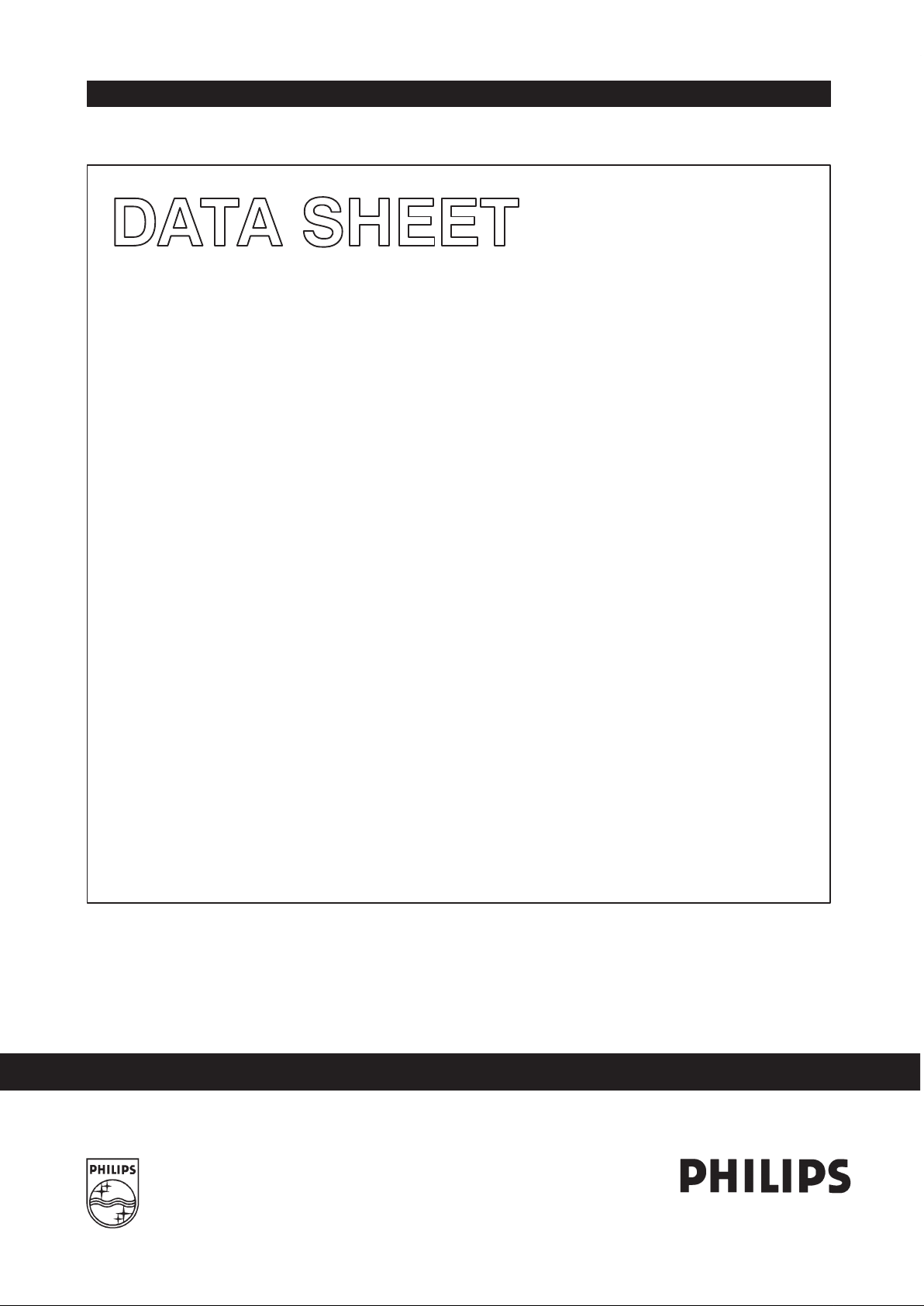
LOGIC DIAGRAM FOR 74F373
V
CC
= Pin 20
GND = Pin 10
D0
D
E
Q
Q0
3
2
D1
D
E
Q
Q1
4
5
D2
D
E
Q
Q2
7
6
D3
D
E
Q
Q3
8
9
D4
D
E
Q
Q4
13
12
D5
D
E
Q
Q5
14
15
D6
D
E
Q
Q6
17
16
D7
D
E
Q
Q7
18
19
11
1
E
OE
SF00256
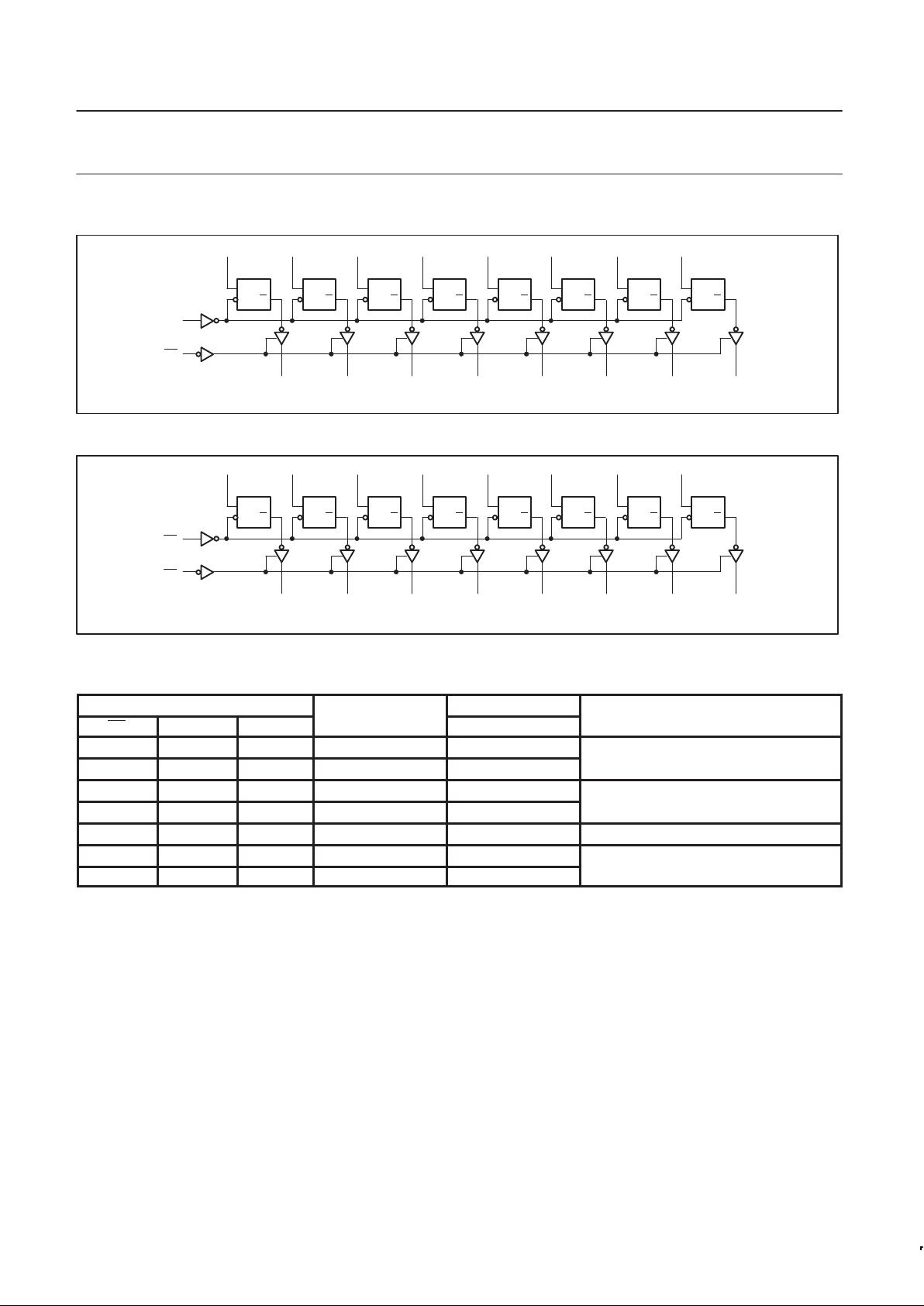
LOGIC DIAGRAM FOR 74F374
VCC = Pin 20
D0
D
CP
Q
Q0
3
2
D1
D
CP
Q
Q1
4
5
D2
D
CP
Q
Q2
7
6
D3
D
CP
Q
Q3
8
9
D4
D
CP
Q
Q4
13
12
D5
D
CP
Q
Q5
14
15
D6
D
CP
Q
Q6
17
16
D7
D
CP
Q
Q7
18
19
11
1
OE
CP
GND = Pin 10
SF00257
FUNCTION TABLE FOR 74F373
INPUTS
INTERNAL
OUTPUTS
OE E Dn
REGISTER
Q0 - Q7
OPERATING MODE
L H L L L
L H H H H
Enable and read register
L ↓ l L L
L ↓ h H H
Latch and read register
L L X NC NC Hold
H L X NC Z
p
H H Dn Dn Z
Disable outputs
NOTES:
H = High-voltage level
h = High state must be present one setup time before the high-to-low enable transition
L = Low-voltage level
l = Low state must be present one setup time before the high-to-low enable transition
NC= No change
X = Don’t care
Z = High impedance “off” state
↓ = High-to-low enable transition
Page 5

Philips Semiconductors Product specification
74F373/74F374Latch/flip-flop
December 5, 1994
5
FUNCTION TABLE FOR 74F374
INPUTS INTERNAL OUTPUTS
OE CP Dn REGISTER Q0 - Q7
OPERATING MODE
L ↑ l L L
L ↑ h H H
Load and read register
L ↑ X NC NC Hold
H ↑ X NC Z
p
H ↑ Dn Dn Z
Disable outputs
NOTES:
H = High-voltage level
h = High state must be present one setup time before the low-to-high clock transition
L = Low-voltage level
l = Low state must be present one setup time before the low-to-high clock transition
NC= No change
X = Don’t care
Z = High impedance “off” state
↑ = Low-to-high clock transition
↑
= Not low-to-high clock transition
ABSOLUTE MAXIMUM RATINGS
(Operation beyond the limit set forth in this table may impair the useful life of the device. Unless otherwise noted these limits are over the
operating free air temperature range.)
SYMBOL
PARAMETER RATING UNIT
V
CC
Supply voltage -0.5 to +7.0 V
V
IN
Input voltage -0.5 to +7.0 V
I
IN
Input current -30 to +5 mA
V
OUT
Voltage applied to output in high output state -0.5 to V
CC
V
I
OUT
Current applied to output in low output state
48 mA
T
amb
Operating free air temperature range 0 to +70 °C
T
stg
Storage temperature range -65 to +150 °C
RECOMMENDED OPERATING CONDITIONS
LIMITS
SYMBOL
PARAMETER
MIN NOM MAX
UNIT
V
CC
Supply voltage
4.5 5.0 5.5 V
V
IH
High-level input voltage 2.0 V
V
IL
Low-level input voltage 0.8 V
I
Ik
Input clamp current -18 mA
I
OH
High-level output current -3 mA
I
OL
Low-level output current
24 mA
T
amb
Operating free air temperature range 0 +70
°C
Page 6

Philips Semiconductors Product specification
74F373/74F374Latch/flip-flop
December 5, 1994
6
DC ELECTRICAL CHARACTERISTICS
(Over recommended operating free-air temperature range unless otherwise noted.)
TEST
LIMITS
SYMBOL
PARAMETER
CONDITIONS
1
MIN TYP2MAX
UNIT
VCC = MIN, VIL = MAX,
±10%V
CC
2.4 V
VOHHigh-l
evel output voltage
VIH = MIN, IOH = MAX
±5%V
CC
2.7 3.4 V
p
VCC = MIN, VIL = MAX, ±10%V
CC
0.35 0.50 V
VOLLow-level output voltage
VIH = MIN, IOL = MAX
±5%V
CC
0.35 0.50 V
V
IK
Input clamp voltage VCC = MIN, II = I
IK
-0.73 -1.2 V
I
I
Input current at maximum input voltage VCC = MAX, VI = 7.0V 100 µA
I
IH
High-level input current VCC = MAX, VI = 2.7V 20 µA
I
IL
Low-level input current VCC = MAX, VI = 0.5V -0.6 mA
I
OZH
Off-state output current, high-level voltage applied VCC = MAX, V
O
= 2.7V 50
µA
I
OZL
Off-state output current, low-level voltage applied VCC = MAX, VO = 0.5V -50
µA
I
OS
Short-circuit output current
3
VCC = MAX -60 -150 mA
pp
74F373
35 60 mA
ICCSupply current (total)
74F374
V
CC
=
MAX
57 86 mA
NOTES:
1. For conditions shown as MIN or MAX, use the appropriate value specified under recommended operating conditions for the applicable type.
2. All typical values are at V
CC
= 5V, T
amb
= 25°C.
3. Not more than one output should be shorted at a time. For testing IOS, the use of high-speed test apparatus and/or sample-and-hold
techniques are preferable in order to minimize internal heating and more accurately reflect operational values. Otherwise, prolonged shorting
of a high output may raise the chip temperature well above normal and thereby cause invalid readings in other parameter tests. In any
sequence of parameter tests, I
OS
tests should be performed last.
AC ELECTRICAL CHARACTERISTICS
LIMITS
T
amb
= +25°C T
amb
= 0°C to +70°C
SYMBOL PARAMETER TEST VCC = +5.0V
VCC = +5.0V ± 10%
UNIT
CONDITION CL = 50pF, RL = 500Ω CL = 50pF, RL = 500Ω
MIN TYP MAX MIN MAX
t
PLH
t
PHL
Propagation delay
Dn to Qn
Waveform 3
3.0
2.0
5.3
3.7
7.0
5.0
3.0
2.0
8.0
6.0
ns
t
PLH
t
PHL
Propagation delay
E to Qn
74F373
Waveform 2
5.0
3.0
9.0
4.0
11.5
7.0
5.0
3.0
12.0
8.0
ns
t
PZH
t
PZL
Output enable time
to high or low level
Waveform 6
Waveform 7
2.0
2.0
5.0
5.6
11.0
7.5
2.0
2.0
11.5
8.5
ns
t
PHZ
t
PLZ
Output disable time
from high or low level
Waveform 6
Waveform 7
2.0
2.0
4.5
3.8
6.5
5.0
2.0
2.0
7.0
6.0
ns
f
max
Maximum clock frequency Waveform 1 150 165 140 ns
t
PLH
t
PHL
Propagation delay
CP to Qn
74F374
Waveform 1
3.5
3.5
5.0
5.0
7.5
7.5
3.0
3.0
8.5
8.5
ns
t
PZH
t
PZL
Output enable time
to high or low level
Waveform 6
Waveform 7
2.0
2.0
9.0
5.3
11.0
7.5
2.0
2.0
12.0
8.5
ns
t
PHZ
t
PLZ
Output disable time
from high or low level
Waveform 6
Waveform 7
2.0
2.0
5.3
4.3
6.0
5.5
2.0
2.0
7.0
6.5
ns
Page 7

Philips Semiconductors Product specification
74F373/74F374Latch/flip-flop
December 5, 1994
7
AC SETUP REQUIREMENTS
LIMITS
T
amb
= +25°C T
amb
= 0°C to +70°C
SYMBOL PARAMETER TEST VCC = +5.0V
VCC = +5.0V ± 10%
UNIT
CONDITION CL = 50pF, RL = 500Ω CL= 50pF, RL = 500Ω
MIN TYP MAX MIN MAX
t
su
(H)
t
su
(L)
Setup time, high or low level
Dn to E
Waveform 4
0
1.0
0
1.0
ns
t
h
(H)
t
h
(L)
Hold time, high or low level
Dn to E
74F373
Waveform 4
3.0
3.0
3.0
3.0
ns
t
w
(H) E Pulse width, high Waveform 1 3.5 4.0 ns
t
su
(H)
t
su
(L)
Setup time, high or low level
Dn to CP
Waveform 5
2.0
2.0
2.0
2.0
ns
t
h
(H)
t
h
(L)
Hold time, high or low level
Dn to CP
74F374
Waveform 5
0
0
0
0
ns
t
w
(H)
t
w
(L)
CP Pulse width,
high or low
Waveform 5
3.5
4.0
3.5
4.0
ns
AC WAVEFORMS
For all waveforms, VM = 1.5V .
The shaded areas indicate when the input is permitted to change for
predictable output performance.
CP
V
M
V
M
V
M
tw(H)
1/f
max
V
M
V
M
t
PHL
tw(L)t
PLH
Qn
SF00258
Waveform 1. Propagation delay for clock input to output,
clock pulse widths, and maximum clock frequency
t
PHL
EV
M
V
M
V
M
tw(H)
V
M
V
M
Qn
t
PLH
SF00259
Waveform 2. Propagation delay for enable to output
and enable pulse width
Dn
V
M
V
M
V
M
V
M
t
PHL
t
PLH
Qn
SF00260
Waveform 3. Propagation delay for data to output
V
M
V
M
V
M
V
M
V
M
V
M
tsu(L) th(L)
t
su
(H) th(H)
E
Dn
SF00261
Waveform 4. Data setup time and hold times
Page 8

Philips Semiconductors Product specification
74F373/74F374Latch/flip-flop
December 5, 1994
8
AC WAVEFORMS (Continued)
For all waveforms, VM = 1.5V .
The shaded areas indicate when the input is permitted to change for
predictable output performance.
V
M
V
M
V
M
V
M
V
M
V
M
tsu(L) th(L)
t
su
(H) th(H)
CP
Dn
SF00262
Waveform 5. Data setup time and hold times
Qn, Qn
V
M
V
M
V
M
t
PHZ
t
PZH
OEn
VOH -0.3V
0V
SF00263
Waveform 6. 3-State output enable time to high level
and output disable time from high level
V
M
V
M
V
M
t
PLZ
t
PZL
VOL +0.3V
OEn
Qn, Q
n
SF00264
Waveform 7. 3-State output enable time to low level
and output disable time from low level
TEST CIRCUIT AND WAVEFORMS
t
w
90%
V
M
10%
90%
V
M
10%
90%
V
M
10%
90%
V
M
10%
NEGATIVE
POSITIVE
t
w
AMP (V)
0V
0V
t
THL (tf
)
INPUT PULSE REQUIREMENTS
rep. rate
t
w
t
TLHtTHL
1MHz 500ns 2.5ns
2.5ns
Input pulse definition
V
CC
family
74F
D.U.T.
GENERATOR
R
L
C
L
R
T
V
IN
V
OUT
Test circuit for 3-state outputs
t
THL (tf
)
t
TLH (tr
)
t
TLH (tr
)
AMP (V)
amplitude
3.0V
1.5V
V
M
R
L
7.0V
SWITCH POSITION
TEST SWITCH
closed
openAll other
t
PLZ
, t
PZL
DEFINITIONS:
Load resistor; see AC electrical characteristics for value.
Load capacitance includes jig and probe capacitance;
see AC electrical characteristics for value.
Termination resistance should be equal to Z
OUT
of pulse
generators.
SF00265
PULSE
PULSE
PULSE
R
L =
C
L =
R
T =
Page 9

Philips Semiconductors Product specification
74F373, 74F374Latch/flip-flop
1994 Dec 05
9
DIP20: plastic dual in-line package; 20 leads (300 mil) SOT146-1
Page 10

Philips Semiconductors Product specification
74F373, 74F374Latch/flip-flop
1994 Dec 05
10
SO20: plastic small outline package; 20 leads; body width 7.5 mm SOT163-1
Page 11

Philips Semiconductors Product specification
74F373, 74F374Latch/flip-flop
1994 Dec 05
11
NOTES
Page 12

Philips Semiconductors FAST Products Product specification
74F373, 74F374Latch/flip-flop
Philips Semiconductors and Philips Electronics North America Corporation reserve the right to make changes, without notice, in the products,
including circuits, standard cells, and/or software, described or contained herein in order to improve design and/or performance. Philips
Semiconductors assumes no responsibility or liability for the use of any of these products, conveys no license or title under any patent, copyright,
or mask work right to these products, and makes no representations or warranties that these products are free from patent, copyright, or mask
work right infringement, unless otherwise specified. Applications that are described herein for any of these products are for illustrative purposes
only. Philips Semiconductors makes no representation or warranty that such applications will be suitable for the specified use without further testing
or modification.
LIFE SUPPORT APPLICA TIONS
Philips Semiconductors and Philips Electronics North America Corporation Products are not designed for use in life support appliances, devices,
or systems where malfunction of a Philips Semiconductors and Philips Electronics North America Corporation Product can reasonably be expected
to result in a personal injury. Philips Semiconductors and Philips Electronics North America Corporation customers using or selling Philips
Semiconductors and Philips Electronics North America Corporation Products for use in such applications do so at their own risk and agree to fully
indemnify Philips Semiconductors and Philips Electronics North America Corporation for any damages resulting from such improper use or sale.
This data sheet contains preliminary data, and supplementary data will be published at a later date. Philips
Semiconductors reserves the right to make changes at any time without notice in order to improve design
and supply the best possible product.
Philips Semiconductors
811 East Arques Avenue
P.O. Box 3409
Sunnyvale, California 94088–3409
Telephone 800-234-7381
DEFINITIONS
Data Sheet Identification Product Status Definition
Objective Specification
Preliminary Specification
Product Specification
Formative or in Design
Preproduction Product
Full Production
This data sheet contains the design target or goal specifications for product development. Specifications
may change in any manner without notice.
This data sheet contains Final Specifications. Philips Semiconductors reserves the right to make changes
at any time without notice, in order to improve design and supply the best possible product.
Philips Semiconductors and Philips Electronics North America Corporation
register eligible circuits under the Semiconductor Chip Protection Act.
Copyright Philips Electronics North America Corporation 1994
All rights reserved. Printed in U.S.A.
(print code) Date of release: July 1994
Document order number: 9397-750-051 19
 Loading...