

Page 1

74F30240
Octal 30Ω line driver with enable,
inverting (open collector)*
74F30244
Octal 30Ω line driver with enable,
non-inverting (open collector)
Product specification
IC15 Data Handbook
1999 Jan 08
INTEGRATED CIRCUITS
* Discontinued part. Please see the Discontinued Product List.
Page 2
Philips Semiconductors Product specification
74F30240*, 74F3024430Ω line drivers
74F30240 Octal 30Ω line driver with enable, inverting (open collector)
74F30244 Octal 30
Ω
line driver with enable, non-inverting (open collecor)
2
1999 Jan 08 853–1 157 20619
* Discontinued part. Please see the Discontinued Products List.
FEA TURES
•Ideal for driving transmission lines or backplanes. 160mA I
OL
ideal
for applications with impedance as low as 30Ω
•Guaranteed threshold voltages on the incident wave while driving
line as low as 30Ω
•High impedance NPN base inputs for reduced loading (20µA in
High and Low states)
•Ideal for applications which require high output drive and minimal
bus loading
•Octal interface
•74F30240 inverting
•74F30244 non-inverting
•Open-Collector outputs sink 160mA
•Multiple side pins are used for V
CC
and GND to reduce lead
inductance (improves speed and noise immunity)
•Available in 24-pin standard slim DIP (300mil) plastic, SOL or
CERDIP packages
DESCRIPTION
The 74F30240 and 74F30244 are high current open collector octal
buffers composed of eight inverters. The 74F30240 has inverting
data paths and the 74F30244 has non-inverting paths. Each device
has eight inverters with two Output Enables (OE
0, OE1), each
controlling four outputs. Both drivers are designed to deal with the
low-impedance transmission line effects found on printed circuit
boards when fast edge rates are used. The 160mA I
OL
provides
ample power to achieve TTL switching voltages on the incident
wave.
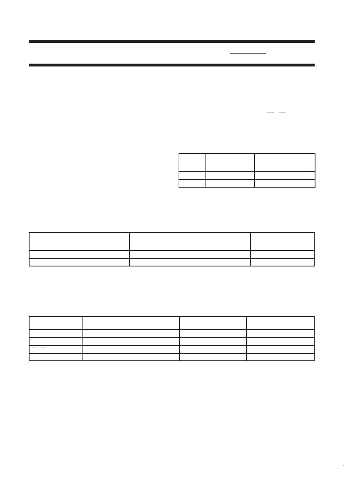
TYPE
TYPICAL
PROPAGATION
DELA Y
TYPICAL
SUPPLY CURRENT
(TOTAL)
74F30240 9.5ns 62.5mA
74F30244 10.5ns 69mA
ORDERING INFORMATION
DESCRIPTION
COMMERCIAL RANGE
VCC = 5V ±10%,
T
amb
= 0°C to +70°C
PACKAGE
DRAWING NUMBER
24-pin Plastic Slim DIP (300mil) N74F30244N SOT222-1
24–pin Plastic SOL
1
N74F30244D SOT137-1
NOTE:
1. Because of the high current sinking capability of these parts, the SOL package should only be used under the following conditions:
a. 50% duty cycle,
AND
b. 3/5 of remaining 50% driving ≤ 100mA (leaving the remaining 2/5 of the drive ≤ 160mA)
OR
c. use ≤ 450 linear feet per minute forced air or other thermal mounting techniques.
INPUT AND OUTPUT LOADING AND FAN-OUT TABLE
PINS DESCRIPTION
74F(U.L.)
HIGH/LOW
LOAD VALUE
HIGH/LOW
D0–D7 Data inputs 1.0/0.033 20µA/20µA
OE0–OE1 Output Enable inputs (Active Low) 1.0/0.033 20µA/20µA
Q0–Q7 Data outputs (OC) for 74F30240 OC/266.7 OC/160mA
Q0–Q7 Data outputs (OC) for 74F30244 OC/266.7 OC/160mA
NOTE: One (1.0) FAST unit load is defined as: 20µA in the High state and 0.6mA in the Low state. OC = Open Collector.
Page 3

Philips Semiconductors Product specification
74F30240*, 74F3024430Ω line drivers
1999 Jan 08
3
* Discontinued part. Please see the Discontinued Products List.
PIN CONFIGURATION – 74F30240
1
2
3
4
5
6
7
8
9
10
11
12 13
14
15
16
17
18
19
20
21
22
23
24Q0
Q
1
Q
2
Q
3
GND
GND
GND
GND
Q
4
Q
5
Q
6
D0
D1
D2
D3
OE
0
V
CC
V
CC
D4
OE
1
D5
D6
D7Q
7
SF01387
PIN CONFIGURATION – 74F30244
1
2
3
4
5
6
7
8
9
10
11
12 13
14
15
16
17
18
19
20
21
22
23
24Q0
Q1
Q2
Q3
GND
GND
GND
GND
Q4
Q5
Q6
D0
D1
D2
D3
OE
0
V
CC
V
CC
D4
OE
1
D5
D6
D7Q7
SF01388
LOGIC SYMBOL – 74F30240
D0 D1 D2 D3 D4 D5 D6 D7
Q0 Q1 Q2 Q3 Q4 Q5 Q6 Q7
20 OE0
17 OE1
24 23 22 21 16 15 14 13
12349101112
V
CC
= PIN 18, 19
GND = PIN 5, 6, 7, 8
SF01389
LOGIC SYMBOL – 74F30244
D0 D1 D2 D3 D4 D5 D6 D7
Q0 Q1 Q2 Q3 Q4 Q5 Q6 Q7
20 OE0
17 OE1
24 23 22 21 16 15 14 13
12349101112
V
CC
= PIN 18, 19
GND = PIN 5, 6, 7, 8
SF01390
IEC/IEEE SYMBOL – 74F30240
124
223
322
421
916
1015
1114
1213
1
20
17
EN1
EN2
SF01391
IEC/IEEE SYMBOL – 74F30244
124
223
322
421
916
1015
1114
1213
1
20
17
EN1
EN2
SF01392
Page 4

Philips Semiconductors Product specification
74F30240*, 74F3024430Ω line drivers
1999 Jan 08
4
* Discontinued part. Please see the Discontinued Products List.
LOGIC DIAGRAM – 74F30240
24
D0
1
Q
0
23
D1
2
Q
1
22
D2
3
Q
2
21
D3
4
Q
3
20
OE
0
VCC = PIN 18, 19
GND = PIN 5, 6, 7, 8
16
D4
9
Q
4
15
D5
10
Q
5
14
D6
11
Q
6
13
D7
12
Q
7
17
OE
1
SF01393
LOGIC DIAGRAM – 74F30244
24
D0
1
Q0
23
D1
2
Q1
22
D2
3
Q2
21
D3
4
Q3
20
OE
0
VCC = PIN 18, 19
GND = PIN 5, 6, 7, 8
16
D4
9
Q4
15
D5
10
Q5
14
D6
11
Q6
13
D7
12
Q7
17
OE
1
SF01394
FUNCTION TABLE
OUTPUTS
INPUTS
74F30240 74F30244
OEn Dn Qn Qn
L L H L
L H L H
H X OFF OFF
H = High voltage level
L = Low voltage level
X = Don’t care
OFF = Pulled up through resistor (Open Collector)
Page 5

Philips Semiconductors Product specification
74F30240*, 74F3024430Ω line drivers
1999 Jan 08
5
* Discontinued part. Please see the Discontinued Products List.
ABSOLUTE MAXIMUM RATINGS
(Operation beyond the limits set forth in this table may impair the useful life of the device.
Unless otherwise noted these limits are over the operating free-air temperature range.)
SYMBOL
PARAMETER RATING UNIT
V
CC
Supply voltage –0.5 to +7.0 V
V
IN
Input voltage –0.5 to +7.0 V
I
IN
Input current –30 to +5 mA
V
OUT
Voltage applied to output in High output state –0.5 to V
CC
V
I
OUT
Current applied to output in Low output state 320 mA
T
amb
Operating free-air temperature range 0 to +70 °C
T
stg
Storage temperature range –65 to +150 °C
RECOMMENDED OPERATING CONDITIONS
LIMITS
SYMBOL
PARAMETER
MIN NOM MAX
UNIT
V
CC
Supply voltage 4.5 5.0 5.5 V
V
IH
High-level input voltage 2.0 V
V
IL
Low-level input voltage 0.8 V
I
IK
Input clamp current –18 mA
V
OH
High-level output voltage 4.5 V
I
OL
Low-level output current 160 mA
T
amb
Operating free-air temperature range 0 +70 °C
DC ELECTRICAL CHARACTERISTICS
(Over recommended operating free-air temperature range unless otherwise noted.)
LIMITS
SYMBOL
PARAMETER
TEST CONDITIONS
1
MIN TYP
2
MAX
UNIT
I
OH
High-level output current
VCC = MIN, VIL = MAX,
VIH = MIN, VOH = MAX
250 µA
IOL = 100mA ±10% V
CC
0.42 0.55 V
V
OL
Low-level output current
V
CC
=
MIN
,
VIL = MAX,
V
IH
= MIN
IOL =
160mA
NO TAG
±5% V
CC
0.80 V
V
IK
Input clamp voltage VCC = MIN, II = I
IK
–0.73 –1.2 V
I
I
Input current at maximum
input voltage
VCC = 0.0V, VI = 7.0V 100 µA
I
IH
High-level input current VCC = MAX, VI = 2.7V 20 µA
I
IL
Low-level input current VCC = MAX, VI = 0.5V –20 µA
I
CCH
13 23 mA
Supply current
74F30240
I
CCL
V
CC
=
MAX
70 95 mA
I
CC
y
(total)
I
CCH
19 27 mA
74F30244
I
CCL
V
CC
=
MAX
70 100 mA
NOTES:
1. For conditions shown as MIN or MAX, use the appropriate value specified under recommended operating conditions for the applicable type.
2. All typical values are at V
CC
= 5V, T
amb
= 25°C.
3. I
OL1
is the current necessary to guarantee the High-to-Low transition in a 30Ω transmission line on the incident wave.
Page 6

Philips Semiconductors Product specification
74F30240*, 74F3024430Ω line drivers
1999 Jan 08
6
* Discontinued part. Please see the Discontinued Products List.
AC ELECTRICAL CHARACTERISTICS
LIMITS
SYMBOL PARAMETER
TEST
CONDITION
T
amb
= +25°C
VCC = +5.0V
C
L
= 50pF, RL = 500Ω
T
amb
= 0°C to +70°C
VCC = +5.0V ± 10%
C
L
= 50pF, RL = 500Ω
UNIT
MIN TYP MAX MIN MAX
t
PLH
t
PHL
Propagation delay
Dn to Qn
Waveform 2
4.0
1.0
10.0
2.0
14.5
5.0
4.0
1.0
15.0
5.5
ns
t
PLH
t
PHL
Propagation delay
OEn to Qn
74f30240
Waveform 1, 2
4.0
3.5
10.0
6.0
14.0
9.0
4.0
3.5
14.5
10.5
ns
t
PLH
t
PHL
Propagation delay
Dn to Qn
Waveform 1
4.0
3.0
10.5
5.5
14.5
9.0
4.0
3.0
15.0
9.5
ns
t
PLH
t
PHL
Propagation delay
OEn to Qn
74f30244
Waveform 1, 2
4.0
3.5
9.5
6.0
14.0
9.0
4.0
3.5
14.5
10.5
ns
AC WAVEFORMS
For all waveforms, VM = 1.5V .
V
M
V
M
V
M
V
M
t
PHL
t
PLH
Dn, OEn
Qn
SF01384
Waveform 1. Propagation Delay for Data to Output
V
M
V
M
V
M
V
M
t
PLH
t
PHL
Dn, OEn
Q
n
SF01385
Waveform 2. Propagation Delay for Data to Output
TYPICAL PROPAGATION DELAYS VERSUS LOAD FOR OPEN COLLECTOR OUTPUTS
NOTE:
When using Open-Collector parts, the value of the pull-up resistor greatly affects the value of the t
PLH
. For example, changing the
specified pull-up resistor value from 500Ω to 100Ω will improve the t
PLH
up to 50% with only a slight increase in the t
PHL
. However,
if the value of the pull-up resistor is changed, the user must make certain that the total I
OL
current through the resistor and the total
I
IL
s of the receivers does not exceed the IOL maximum specification.
t
PLH
t
PHL
6005004003002001000
0
1
2
3
4
5
6
7
8
9
LOAD RESISTOR (Ω)
PROPAGATION DELAY (ns)
SF01386
Page 7

Philips Semiconductors Product specification
74F30240*, 74F3024430Ω line drivers
1999 Jan 08
7
* Discontinued part. Please see the Discontinued Products List.
TEST CIRCUIT AND WAVEFORMS
t
w
90%
V
M
10%
90%
V
M
10%
90%
V
M
10%
90%
V
M
10%
NEGATIVE
PULSE
POSITIVE
PULSE
t
w
AMP (V)
0V
0V
t
THL (tf
)
INPUT PULSE REQUIREMENTS
rep. rate
t
w
t
TLHtTHL
1MHz 500ns
2.5ns 2.5ns
Input Pulse Definition
V
CC
family
74F
D.U.T.
PULSE
GENERATOR
R
L
C
L
R
T
V
IN
V
OUT
Test Circuit for Open Collector Outputs
DEFINITIONS:
R
L
= Load resistor;
see AC electrical characteristics for value.
C
L
= Load capacitance includes jig and probe capacitance;
see AC electrical characteristics for value.
R
T
= Termination resistance should be equal to Z
OUT
of
pulse generators.
t
THL (tf
)
t
TLH (tr
)
t
TLH (tr
)
AMP (V)
amplitude
3.0V 1.5V
V
M
R
L
7.0V
SF00027
Page 8

Philips Semiconductors Product specification
74F30240*, 74F3024430Ω line drivers
1999 Jan 08
8
* Discontinued part. Please see the Discontinued Product List.
DIP24: plastic dual in-line package; 24 leads (300 mil) SOT222-1
Page 9

Philips Semiconductors Product specification
74F30240*, 74F3024430Ω line drivers
1999 Jan 08
9
* Discontinued part. Please see the Discontinued Product List.
SO24: plastic small outline package; 24 leads; body width 7.5 mm SOT137-1
Page 10

Philips Semiconductors Product specification
74F30240*, 74F3024430Ω line drivers
1999 Jan 08
10
* Discontinued part. Please see the Discontinued Product List.
Definitions
Short-form specification — The data in a short-form specification is extracted from a full data sheet with the same type number and title. For
detailed information see the relevant data sheet or data handbook.
Limiting values definition — Limiting values given are in accordance with the Absolute Maximum Rating System (IEC 134). Stress above one
or more of the limiting values may cause permanent damage to the device. These are stress ratings only and operation of the device at these or
at any other conditions above those given in the Characteristics sections of the specification is not implied. Exposure to limiting values for extended
periods may affect device reliability.
Application information — Applications that are described herein for any of these products are for illustrative purposes only. Philips
Semiconductors make no representation or warranty that such applications will be suitable for the specified use without further testing or
modification.
Disclaimers
Life support — These products are not designed for use in life support appliances, devices or systems where malfunction of these products can
reasonably be expected to result in personal injury . Philips Semiconductors customers using or selling these products for use in such applications
do so at their own risk and agree to fully indemnify Philips Semiconductors for any damages resulting from such application.
Right to make changes — Philips Semiconductors reserves the right to make changes, without notice, in the products, including circuits, standard
cells, and/or software, described or contained herein in order to improve design and/or performance. Philips Semiconductors assumes no
responsibility or liability for the use of any of these products, conveys no license or title under any patent, copyright, or mask work right to these
products, and makes no representations or warranties that these products are free from patent, copyright, or mask work right infringement, unless
otherwise specified.
Philips Semiconductors
811 East Arques Avenue
P.O. Box 3409
Sunnyvale, California 94088–3409
Telephone 800-234-7381
Copyright Philips Electronics North America Corporation 1998
All rights reserved. Printed in U.S.A.
Date of release: 03-98
Document order number: 9397-750-05213
Data sheet
status
Objective
specification
Preliminary
specification
Product
specification
Product
status
Development
Qualification
Production
Definition
[1]
This data sheet contains the design target or goal specifications for product development.
Specification may change in any manner without notice.
This data sheet contains preliminary data, and supplementary data will be published at a later date.
Philips Semiconductors reserves the right to make chages at any time without notice in order to
improve design and supply the best possible product.
This data sheet contains final specifications. Philips Semiconductors reserves the right to make
changes at any time without notice in order to improve design and supply the best possible product.
Data sheet status
[1] Please consult the most recently issued datasheet before initiating or completing a design.
* Discontinued part. Please see the Discontinued Product List.
 Loading...