

Page 1

INTEGRATED CIRCUITS
74F2373
Octal transparent latch with 30Ω
equivalent output termination (3-State)
Product specification
Supersedes data of 1995 Jun 20
IC15 Data Handbook
1999 Feb 01
Page 2
Philips Semiconductors Product specification
Octal transparent latch with 30Ω equivalent output
termination (3-State)
FEA TURES
•8-bit transparent latch
•30 Ohm output termination for driving DRAM
•3-State outputs glitch free during power-up and power-down
•Common 3-State output register
•Independent register and 3-State buffer operation
DESCRIPTION
The 74F2373 is an octal transparent latch coupled to eight 3-State
output devices. The two sections of the device are controlled
independently by enable (E) and output enable (OE
The 30 Ohm series termination on the outputs reduces
over/undershoot, making them ideal for driving DRAM
ORDERING INFORMATION
DESCRIPTION COMMERCIAL RANGE DRAWING NUMBER
20-pin plastic DIP N74F2373N SOT146-1
20-pin plastic SOL N74F2373D SOT163-1
) control gates.
VCC = 5V ±10%, T
ORDER CODE
The data on the D inputs is transferred to the latch outputs when the
enable (E) input is high. The latch remains transparent to the data
input while E is high, and stores the data that is present one setup
time before the high-to-low enable transition.
The 3-State output buffers are designed to drive heavily loaded
3-State buses, MOS memories, or MOS microprocessors.
The active low output enable (OE
independent of the latch operation. When OE
transparent data appears at the output.
When OE
is high, the outputs are in high impedance “off” state,
which means they will neither drive nor load the bus.
TYPE
74F2373 4.5ns 35mA
= 0°C to +70°C
amb
) controls all eight 3-State buffers
TYPICAL
PROPAGATION
DELA Y
74F2373
is low, latched or
TYPICAL SUPPL Y
CURRENT
(TOTAL)
INPUT AND OUTPUT LOADING AND FAN OUT TABLE
PINS DESCRIPTION
D0 - D7 Data inputs 1.0/1.0
E Enable input (active high) 1.0/1.0
OE Output enable inputs (active low) 1.0/1.0
Q0 - Q7 3-State outputs 150/40 3.0mA/3.0mA
NOTE: One (1.0) FAST unit load is defined as: 20µA in the high state and 0.6mA in the low state.
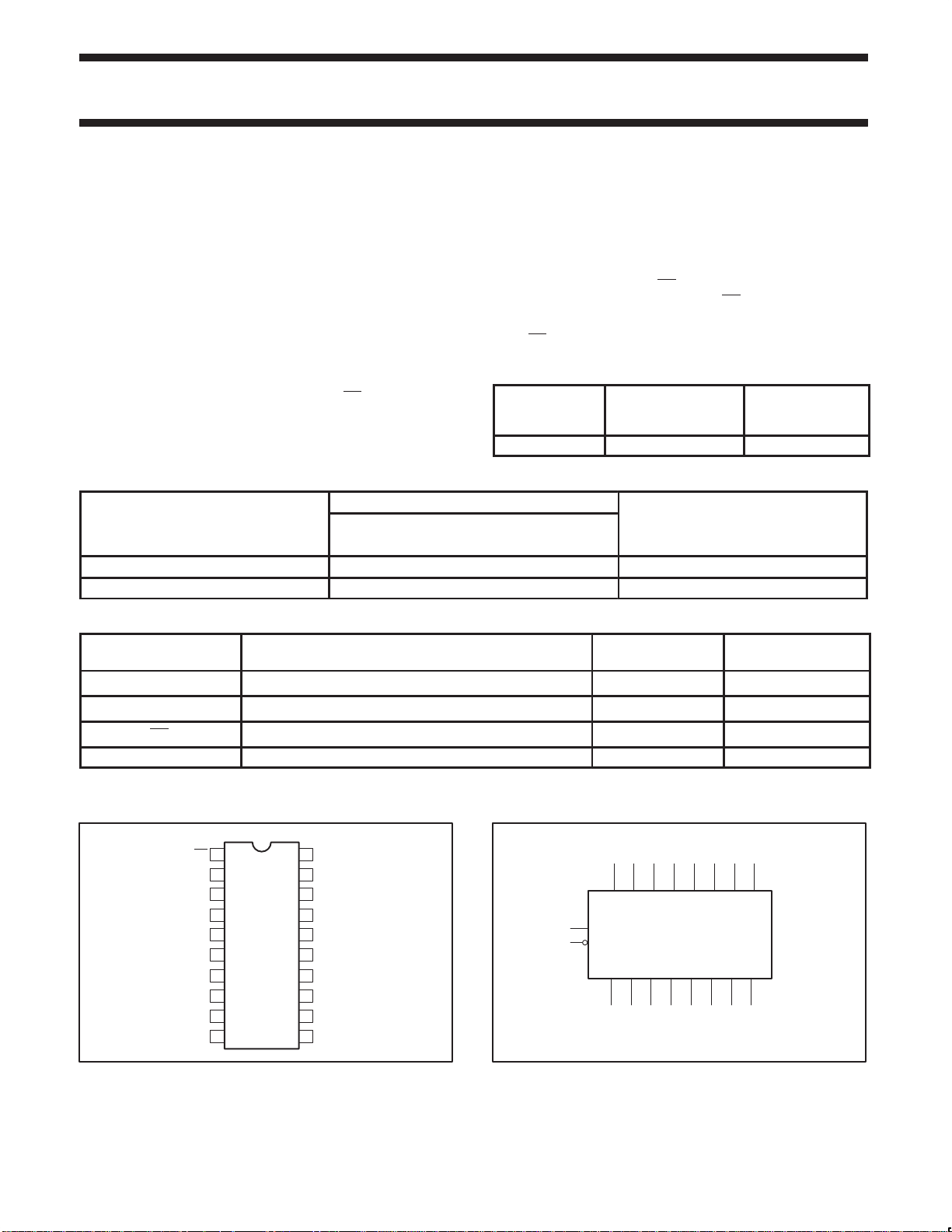
PIN CONFIGURATION
OE
1
2
Q0
3
D0
4
D1
5
Q1
6
Q2
7
D2
8
D3
9
Q3
10 11
GND
20
V
CC
19
Q7
18
D7
17
D6
16
Q6
15
Q5
14
D5
13
D4
12
Q4
E
SF00250
LOGIC SYMBOL
11
E
OE
1
= Pin 20
V
CC
GND = Pin 10
74F (U.L.)
HIGH/LOW
3 4 7 8 13 14 17 18
D0 D1 D2 D3 D4 D5 D6 D7
Q0 Q1 Q2 Q3 Q4 Q5 Q6 Q7
2 5 6 9 12 15 16 19
SF00251
LOAD VALUE
HIGH/LOW
20µA/0.6mA
20µA/0.6mA
20µA/0.6mA
1999 Feb 01 853-2140 20747
2
Page 3
Philips Semiconductors Product specification
OPERATING MODE
Enable and read register
Latch and read register
Disable outputs
Octal transparent latch with 30Ω equivalent output
termination (3-State)
IEC/IEEE SYMBOL
1
11
3
4
7
8
13
14
17
18
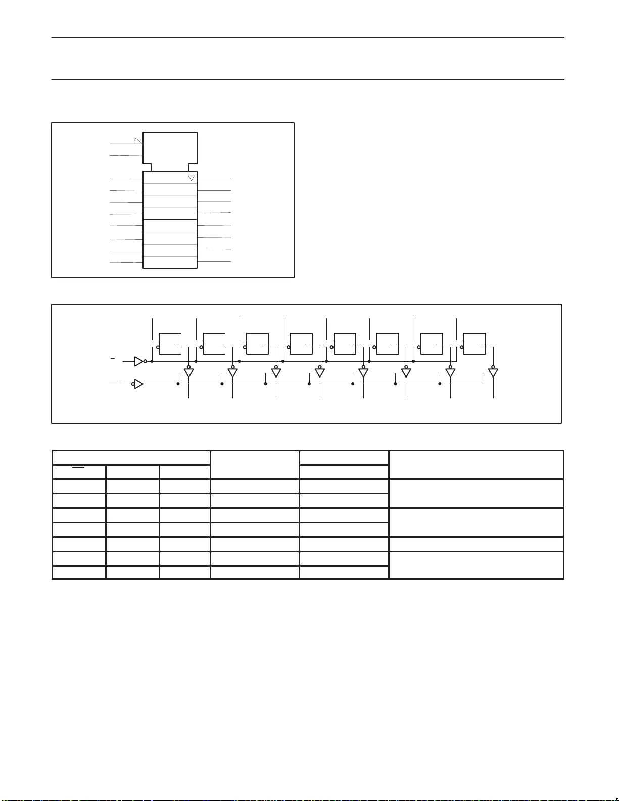
LOGIC DIAGRAM
E
EN1
EN2
SF00252
4
D
E
2
5
6
9
12
15
16
19
D2
7
Q
D
E
D3
8
Q
D
E
D4
13
Q
D
E
2D
D0
11
1
3
D
E
D1
Q
74F2373
D5
14
D
Q
E
D6
17
Q
E
D7
18
D
D
Q
Q
E
1
V
= Pin 20
CC
GND = Pin 10
OE
Q0
2
Q1
5
Q2
6
Q3
9
Q4
FUNCTION TABLE
INPUTS
OE E Dn
INTERNAL
REGISTER
L H L L L
L H H H H
L ↓ l L L
L ↓ h H H
L L X NC NC Hold
H L X NC Z
H H Dn Dn Z
NOTES:
H = High-voltage level
h = High state must be present one setup time before the high-to-low enable transition
L = Low-voltage level
l = Low state must be present one setup time before the high-to-low enable transition
NC= No change
X = Don’t care
Z = High impedance “off” state
↓ = High-to-low enable transition
OUTPUTS
Q0 - Q7
12
Q5
15
Q6
16
19
Q7
SF00256
p
1999 Feb 01
3
Page 4

Philips Semiconductors Product specification
SYMBOL
PARAMETER
UNIT
SYMBOL
PARAMETER
UNIT
VOHHigh-level output voltage
VOLLow-level out ut voltage
3
Octal transparent latch with 30Ω equivalent output
termination (3-State)
ABSOLUTE MAXIMUM RATINGS
(Operation beyond the limit set forth in this table may impair the useful life of the device. Unless otherwise noted these limits are over the
operating free air temperature range.)
SYMBOL
V
V
I
IN
V
I
OUT
T
T
CC
IN
OUT
amb
stg
Supply voltage –0.5 to +7.0 V
Input voltage –0.5 to +7.0 V
Input current –30 to +5 mA
Voltage applied to output in high output state -0.5 to V
Current applied to output in low output state
Operating free air temperature range 0 to +70 °C
Storage temperature range –65 to +150 °C
RECOMMENDED OPERATING CONDITIONS
V
CC
V
IH
V
IL
I
Ik
I
OH
I
OL
T
amb
* 12mA with reduced noise margin
Supply voltage
High-level input voltage 2.0 V
Low-level input voltage 0.8 V
Input clamp current –18 mA
High-level output current –3* mA
Low-level output current
Operating free air temperature range 0 +70
PARAMETER RATING UNIT
LIMITS
MIN NOM MAX
4.5 5.0 5.5 V
74F2373
CC
24 mA
5* mA
V
°C
DC ELECTRICAL CHARACTERISTICS
(Over recommended operating free-air temperature range unless otherwise noted.)
LIMITS
MIN TYP2MAX
2.4 V
2.7 3.4 V
2.0 V
2.0 V
0.42 0.50 V
0.42 0.50 V
0.67 V
0.67 V
-0.73 -1.2 V
µA
µA
V
I
I
I
IH
I
IL
I
OZH
I
OZL
I
OS
I
CC
TEST
CONDITIONS
VCC = MIN, VIL = MAX,
VIH = MIN, IOH = –3mA
p
VCC = MIN, VIL = MAX,
VIH = MIN, IOH = –12mA
VCC = MIN, VIL = MAX, ±10%V
p
VIH = MIN, IOL = –5mA
VCC = MIN, VIL = MAX, ±10%V
VIH = MIN, IOL = 12mA
IK
Input clamp voltage VCC = MIN, II = I
IK
Input current at maximum input voltage VCC = MAX, VI = 7.0V 100 µA
High-level input current VCC = MAX, VI = 2.7V 20 µA
Low-level input current VCC = MAX, VI = 0.5V -0.6 mA
Off-state output current, high-level voltage applied VCC = MAX, V
= 2.7V 50
O
Off-state output current, low-level voltage applied VCC = MAX, VO = 0.5V -50
Short-circuit output current
VCC = MAX -60 -150 mA
Supply current (total) VCC = MAX 35 60 mA
1
±10%V
±5%V
±10%V
±5%V
±5%V
±5%V
CC
CC
CC
CC
CC
CC
CC
CC
NOTES:
1. For conditions shown as MIN or MAX, use the appropriate value specified under recommended operating conditions for the applicable type.
2. All typical values are at V
3. Not more than one output should be shorted at a time. For testing I
techniques are preferable in order to minimize internal heating and more accurately reflect operational values. Otherwise, prolonged shorting
= 5V, T
CC
amb
= 25°C.
, the use of high-speed test apparatus and/or sample-and-hold
OS
of a high output may raise the chip temperature well above normal and thereby cause invalid readings in other parameter tests. In any
sequence of parameter tests, IOS tests should be performed last.
1999 Feb 01
4
Page 5

Philips Semiconductors Product specification
Octal transparent latch with 30Ω equivalent output
termination (3-State)
AC ELECTRICAL CHARACTERISTICS
LIMITS
T
= +25°C T
amb
SYMBOL PARAMETER TEST VCC = +5.0V
CONDITION CL = 50pF, RL = 500Ω CL = 50pF, RL = 500Ω
MIN TYP MAX MIN MAX
t
PLH
t
PHL
t
PLH
t
PHL
t
PZH
t
PZL
t
PHZ
t
PLZ
Propagation delay
Dn to Qn
Propagation delay
E to Qn
Output enable time
to high or low level
Output disable time
from high or low level
Waveform 2
Waveform 1
Waveform 4
Waveform 5
Waveform 4
Waveform 5
3.0
2.0
5.0
3.0
2.0
2.0
2.0
2.0
5.3
3.7
9.0
4.0
5.0
5.6
4.5
3.8
8.0
6.0
12.0
8.0
12.0
8.0
6.5
5.5
AC SETUP REQUIREMENTS
LIMITS
T
= +25°C T
amb
SYMBOL PARAMETER TEST VCC = +5.0V
CONDITION CL = 50pF, RL = 500Ω CL= 50pF, RL = 500Ω
MIN TYP MAX MIN MAX
t
(H)
su
t
(L)
su
t
(H)
h
t
(L)
h
t
(H) E Pulse width, high Waveform 1 3.5 4.0 ns
w
Setup time, high or low level
Dn to E
Hold time, high or low level
Dn to E
Waveform 3
Waveform 3
0
1.0
3.0
3.0
= 0°C to +70°C
amb
VCC = +5.0V ± 10%
3.0
2.0
5.0
3.0
2.0
2.0
2.0
2.0
= 0°C to +70°C
amb
VCC = +5.0V ± 10%
0
1.0
3.0
3.0
74F2373
9.0
7.0
12.5
8.5
12.5
8.5
7.5
6.5
UNIT
ns
ns
ns
ns
UNIT
ns
ns
AC WAVEFORMS
For all waveforms, VM = 1.5V.
The shaded areas indicate when the input is permitted to change for predictable output performance.
tw(H)
EV
Qn
M
t
PHL
V
M
V
M
V
t
M
PLH
V
M
Waveform 1. Propagation delay for enable to output
and enable pulse width
Dn
Qn
V
M
t
PLH
V
M
t
PHL
V
V
M
M
SF00260
Waveform 2. Propagation delay for data to output
SF00259
Dn
E
V
M
t
(H) th(H)
su
V
M
V
M
Waveform 3. Data setup time and hold times
OEn
Qn, Qn
V
t
PZH
M
Waveform 4. 3-State output enable time to high level
and output disable time from high level
V
tsu(L) th(L)
V
M
t
PHZ
V
M
V
M
M
V
M
VOH -0.3V
SF00261
0V
SF00263
1999 Feb 01
5
Page 6

Philips Semiconductors Product specification
Octal transparent latch with 30Ω equivalent output
termination (3-State)
AC WAVEFORMS (Continued)
For all waveforms, VM = 1.5V.
The shaded areas indicate when the input is permitted to change for
predictable output performance.
OEn
Qn, Q
n
Waveform 5. 3-State output enable time to low level
TEST CIRCUIT AND WAVEFORMS
SWITCH POSITION
TEST SWITCH
, t
t
PLZ
PZL
PULSE
GENERATOR
DEFINITIONS:
R
Load resistor; see AC electrical characteristics for value.
L =
C
Load capacitance includes jig and probe capacitance;
L =
see AC electrical characteristics for value.
R
Termination resistance should be equal to Z
T =
generators.
V
t
PZL
M
V
V
M
t
PLZ
M
and output disable time from low level
V
closed
CC
openAll other
V
IN
R
T
D.U.T.
V
OUT
R
R
C
L
Test circuit for 3-state outputs
OUT
VOL +0.3V
SF00264
L
L
of pulse
7.0V
NEGATIVE
PULSE
POSITIVE
PULSE
family
74F
90%
10%
amplitude
3.0V
t
w
V
M
10%
)
t
THL (tf
t
)
TLH (tr
90%
V
M
t
w
t
TLH (tr
t
THL (tf
10%
)
)
90%
Input pulse definition
INPUT PULSE REQUIREMENTS
V
1.5V
rep. rate
M
1MHz 500ns 2.5ns
t
w
V
M
V
M
74F2373
90%
10%
t
TLHtTHL
2.5ns
AMP (V)
0V
AMP (V)
0V
1999 Feb 01
SF00265
6
Page 7

Philips Semiconductors Product specification
Octal transparent latch with 30Ω equivalent output
74F2373
termination (3-State)
DIP20: plastic dual in-line package; 20 leads (300 mil) SOT146-1
1999 Feb 01
7
Page 8

Philips Semiconductors Product specification
Octal transparent latch with 30Ω equivalent output
74F2373
termination (3-State)
SO20: plastic small outline package; 20 leads; body width 7.5 mm SOT163-1
1999 Feb 01
8
Page 9

Philips Semiconductors Product specification
Octal transparent latch with 30Ω equivalent output
termination (3-State)
NOTES
74F2373
1999 Feb 01
9
Page 10

Philips Semiconductors Product specification
Octal transparent latch with 30Ω equivalent output
termination (3-State)
Data sheet status
Data sheet
status
Objective
specification
Preliminary
specification
Product
specification
Product
status
Development
Qualification
Production
Definition
This data sheet contains the design target or goal specifications for product development.
Specification may change in any manner without notice.
This data sheet contains preliminary data, and supplementary data will be published at a later date.
Philips Semiconductors reserves the right to make chages at any time without notice in order to
improve design and supply the best possible product.
This data sheet contains final specifications. Philips Semiconductors reserves the right to make
changes at any time without notice in order to improve design and supply the best possible product.
[1]
74F2373
[1] Please consult the most recently issued datasheet before initiating or completing a design.
Definitions
Short-form specification — The data in a short-form specification is extracted from a full data sheet with the same type number and title. For
detailed information see the relevant data sheet or data handbook.
Limiting values definition — Limiting values given are in accordance with the Absolute Maximum Rating System (IEC 134). Stress above one
or more of the limiting values may cause permanent damage to the device. These are stress ratings only and operation of the device at these or
at any other conditions above those given in the Characteristics sections of the specification is not implied. Exposure to limiting values for extended
periods may affect device reliability.
Application information — Applications that are described herein for any of these products are for illustrative purposes only. Philips
Semiconductors make no representation or warranty that such applications will be suitable for the specified use without further testing or
modification.
Disclaimers
Life support — These products are not designed for use in life support appliances, devices or systems where malfunction of these products can
reasonably be expected to result in personal injury . Philips Semiconductors customers using or selling these products for use in such applications
do so at their own risk and agree to fully indemnify Philips Semiconductors for any damages resulting from such application.
Right to make changes — Philips Semiconductors reserves the right to make changes, without notice, in the products, including circuits, standard
cells, and/or software, described or contained herein in order to improve design and/or performance. Philips Semiconductors assumes no
responsibility or liability for the use of any of these products, conveys no license or title under any patent, copyright, or mask work right to these
products, and makes no representations or warranties that these products are free from patent, copyright, or mask work right infringement, unless
otherwise specified.
Philips Semiconductors
811 East Arques Avenue
P.O. Box 3409
Sunnyvale, California 94088–3409
Telephone 800-234-7381
Copyright Philips Electronics North America Corporation 1998
All rights reserved. Printed in U.S.A.
print code Date of release: 10-98
Document order number: 9397-750-05201
yyyy mmm dd
10
 Loading...