

Page 1
Philips Semiconductors Product specification
74F193Up/down binary counter with separate up/down clocks
1
1995 Jul 17
853-0353 15459
FEATURES
•Synchronous reversible 4-bit counting
•Asynchronous parallel load capability
•Asynchronous reset (clear)
•Cascadable without external logic
DESCRIPTION
The 74F193 is a 4-bit synchronous up/down counter in the binary
mode. Separate up/down clocks, CP
U
and CPD respectively,
simplify operation. The outputs change state synchronously with the
Low-to-High transition of either clock input. If the CP
U
clock is
pulsed while CP
D
is held High, the device will count up. If CPD clock
is pulsed while CP
U
is held High, the device will count down. The
device can be cleared at any time by the asynchronous reset pin. It
may also be loaded in parallel by activating the asynchronous
parallel load pin.
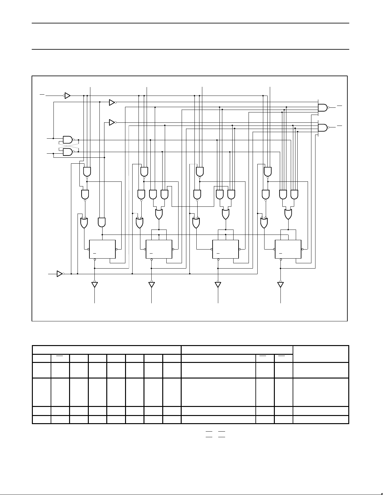
Inside the device are four master-slave JK flip-flops with the
necessary steering logic to provide the asynchronous reset,
asynchronous preset, load, and synchronous count up and count
down functions.
Each flip-flop contains JK feedback from slave to master, such that a
Low-to-High transition on the CP
D
input will decrease the count by
one, while a similar transition on the CP
U
input will advance the
count by one.
One clock should be held High while counting with the other,
because the circuit will either count by twos or not at all, depending
on the state of the first JK flip-flop, which cannot toggle as long as
either clock input is Low. Applications requiring reversible operation
must make the reversing decision while the activating clock is High
to avoid erroneous counts.
The Terminal Count Up (TC
U
) and Terminal Count Down (TCD)
outputs are normally High. When the circuit has reached the
maximum count state of 15, the next High-to-Low transition of CP
U
will cause TCU to go Low. TCU will stay Low until CPU goes High
again, duplicating the count up clock, although delayed by two gate
delays. Likewise, the TC
D
output will go Low when the circuit is in
the zero state and the CP
D
goes Low. The TC outputs can be used
as the clock input signals to the next higher order circuit in a
multistage counter, since they duplicate the clock waveforms.
Multistage counters will not be fully synchronous since there is a
two-gate delay time difference added for each stage that is added.
The counter may be preset by the asynchronous parallel load
capability of the circuit. Information present on the parallel Data
inputs (D0 - D3) is loaded into the counter and appears on the
outputs regardless of the conditions of the clock inputs when the
Parallel Load (PL
) input is Low. A High level on the Master Reset
(MR) input will disable the parallel load gates, override both clock
inputs, and set all Q outputs Low. If one of the clock inputs is Low
during and after a reset or load operation, the next Low-to-High
transition of the clock will be interpreted as a legitimate signal and
will be counted.
TYPE
TYPICAL f
MAX
TYPICAL
SUPPLY CURRENT
(TOTAL)
74F193 125MHz 32mA
ORDERING INFORMATION
DESCRIPTION
COMMERCIAL RANGE
V
CC
= 5V ±10%, T
amb
= 0°C to +70°C
16-pin plastic DIP N74F193N
16-pin plastic SO N74F193D
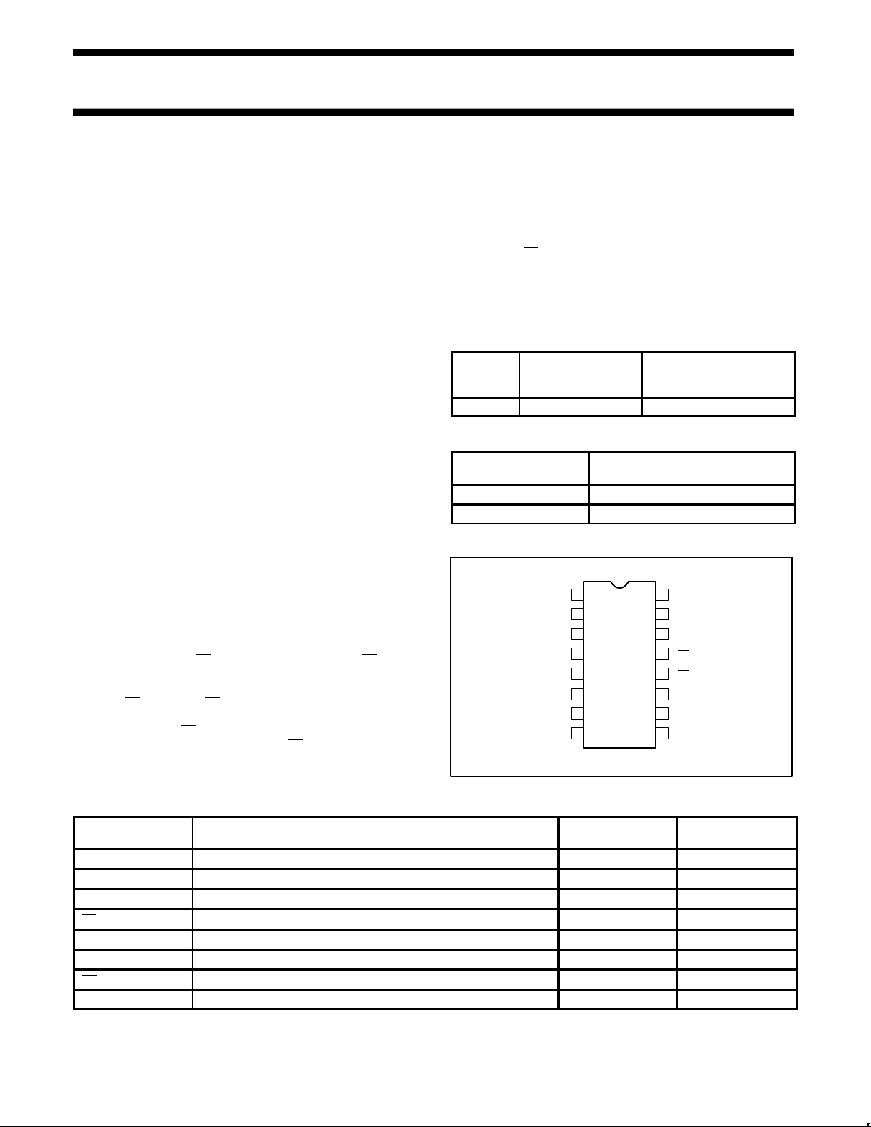
PIN CONFIGURATION
16
15
14
13
12
11
10
98
7
6
5
4
3
2
1D1
Q1
Q0
CP
D
CP
U
Q2
Q3
D0
TC
D
TC
U
D2
D3
PL
GND
MR
V
CC
SF00745
INPUT AND OUTPUT LOADING AND FAN-OUT TABLE
PINS DESCRIPTION
74F(U.L.)
HIGH/LOW
LOAD VALUE
HIGH/LOW
D0 - D3 Data inputs 1.0/1.0 20µA/0.6mA
CP
U
Count up clock input (active rising edge) 1.0/3.0 20µA/1.8mA
CP
D
Count down clock input (active rising edge) 1.0/3.0 20µA/1.8mA
PL Asynchronous parallel load control input (active Low) 1.0/1.0 20µA/0.6mA
MR Asynchronous master reset input 1.0/1.0 20µA/0.6mA
Q0 - Q3 Flip-flop outputs 50/33 1.0mA/20mA
TC
U
Terminal count up (carry) output (active Low) 50/33 1.0mA/20mA
TC
D
Terminal count down (borrow) output (active Low) 50/33 1.0mA/20mA
NOTE: One (1.0) FAST Unit Load (U.L.) is defined as: 20µA in the High state and 0.6mA in the Low state.
Page 2
Philips Semiconductors Product specification
74F193Up/down binary counter with separate up/down clocks
1995 Jul 17
2
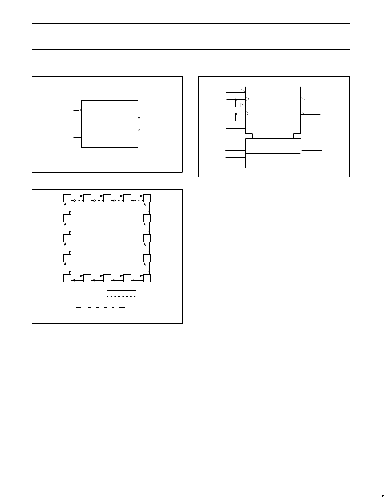
LOGIC SYMBOL
VCC = Pin 16
GND = Pin 8
11
15 1 10 9
7623
14
4
5
CP
U
CP
D
Q0
D0 D1Q1D2
Q2 Q3
D3
PL
12
13
MR
TC
U
TC
D
SF00746
STATE DIAGRAM
TCU = Q0 . Q1 . Q2 . Q3 . CP
U
TCD = Q0 . Q1 . Q2 . Q3 . CP
D
Logic Equations for Terminal Count
COUNT UP
COUNT DOWN
0 1 2 3 4
5
6
7
89101112
13
14
15
SF00748
LOGIC SYMBOL (IEEE/IEC)
11
5
4
14
[1]
R
15
1
10
9
3D
3
2
6
7
1–
G2
C3
SF00747
2+
G1
CTR DIV 16
[2]
[4]
[8]
12
13
1CT=15
2CT=0
Page 3
Philips Semiconductors Product specification
74F193Up/down binary counter with separate up/down clocks
1995 Jul 17
3
LOGIC DIAGRAM
12
13
J
Q
CP
Q
S
D
R
D
KJ
Q
CP
Q
S
D
R
D
D0 D1 D3
Q1Q0
CP
D
PL
15 1
23
14
4
11
V
CC
= Pin 16
GND = Pin 8
KJ
Q
CP
Q
S
D
R
D
Q1
10
6
K
JQCP
Q
S
D
R
D
Q1
9
7
MR
CP
U
5
TC
U
TC
D
D2
SF00749
FUNCTION TABLE
INPUTS OUTPUTS OPERATING
MR PL CPUCP
D
D0 D1 D2 D3 Q0 Q1 Q2 Q3 TCUTC
D
MODE
H X X L X X X X L L L L H L Reset (clear)
H X X H X X X X L L L L H H
L L X L L L L L L L L L H L
L L X H L L L L L L L L H H Parallel load
L L L X H H H H H H H H L H
L L H X H H H H H H H H H H
L H ↑ H X X X X Count up H
1
H Count up
L H H ↑ X X X X Count down H H2Count down
H = High voltage level
L = Low voltage level
X = Don’t care
↑ = Low-to-High clock transition
NOTES:
1. TC
U
=CPU at terminal count up (HHHH)
2. TC
D
=CPD at terminal count down (LLLL)
Page 4
Philips Semiconductors Product specification
74F193Up/down binary counter with separate up/down clocks
1995 Jul 17
4
ABSOLUTE MAXIMUM RATINGS
(Operation beyond the limits set forth in this table may impair the useful life of the device. Unless otherwise noted these limits are over the
operating free-air temperature range.)
SYMBOL
PARAMETER RATING UNIT
V
CC
Supply voltage –0.5 to +7.0 V
V
IN
Input voltage –0.5 to +7.0 V
I
IN
Input current –30 to +5.0 mA
V
OUT
Voltage applied to output in High output state –0.5 to +V
CC
V
I
OUT
Current applied to output in Low output state 40 mA
T
amb
Operating free-air temperature range 0 to +70
°
C
T
stg
Storage temperature –65 to +150
°
C
RECOMMENDED OPERATING CONDITIONS
LIMITS
SYMBOL
PARAMETER
MIN NOM MAX
UNIT
V
CC
Supply voltage 4.5 5.0 5.5 V
V
IH
High-level input voltage 2.0 V
V
IL
Low-level input voltage 0.8 V
I
IK
Input clamp current –18 mA
I
OH
High-level output current –1 mA
I
OL
Low-level output current 20 mA
T
amb
Operating free-air temperature range 0 +70
°
C
DC ELECTRICAL CHARACTERISTICS
(Over recommended operating free-air temperature range unless otherwise noted.)
LIMITS
SYMBOL
PARAMETER
TEST CONDITIONS
1
MIN TYP
2
MAX
UNIT
V
MIN, V
MAX,
10%V
CC
2.5 V
VOHHigh-level output voltage
VCC MIN, VIL MAX,
I
OH
= MAX, VIH = MIN
5%V
CC
2.7 3.4 V
V
MIN, V
MAX,
10%V
CC
0.35 0.50 V
VOLLow-level output voltage
VCC MIN, VIL MAX,
IOL = MAX, VIH = MIN
5%V
CC
0.35 0.50 V
V
IK
Input clamp voltage VCC = MIN, II = I
IK
–0.73 –1.2 V
I
I
Input current atmaximum
input voltage
VCC = MAX, VI = 7.0V 100 µA
I
IH
High-level input current VCC = MAX, VI = 2.7V 20 µA
I
IL
Low-level input
CPU, CP
D
–1.8 mA
Low-level input
current
Others
VCC = MAX, VI = 0.5V
–0.6 mA
I
OS
Short-circuit output current
3
VCC = MAX –60 –150 mA
I
CC
Supply current (total)
4
VCC = MAX 32 50 mA
NOTES:
1. For conditions shown as MIN or MAX, use the appropriate value specified under recommended operating conditions for the applicable type.
2. All typical values are at V
CC
= 5V, T
amb
= 25°C.
3. Not more than one output should be shorted at a time. For testing I
OS
, the use of high-speed test apparatus and/or sample-and-hold
techniques are preferable in order to minimize internal heating and more accurately reflect operational values. Otherwise, prolonged shorting
of a High output may raise the chip temperature well above normal and thereby cause invalid readings in other parameter tests. In any
sequence of parameter tests, I
OS
tests should be performed last.
4. Measure I
CC
with parallel load and Master reset inputs grounded, all other inputs at 4.5V and all outputs open.
Page 5
Philips Semiconductors Product specification
74F193Up/down binary counter with separate up/down clocks
1995 Jul 17
5
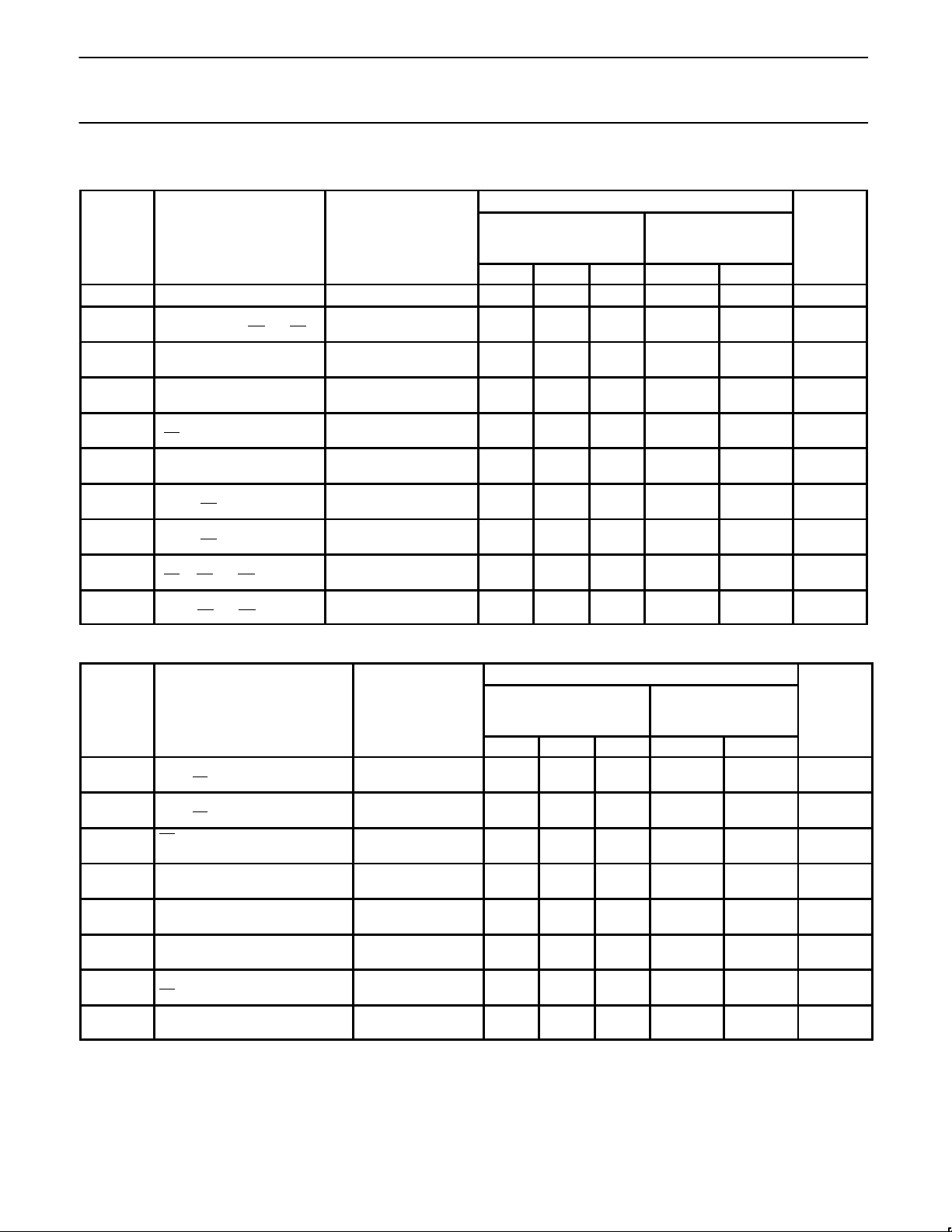
AC ELECTRICAL CHARACTERISTICS
LIMITS
SYMBOL
PARAMETER
TEST CONDITIONS
T
amb
= +25°C
VCC = +5.0V
C
L
= 50pF, RL = 500Ω
T
amb
= 0°C to +70°C
VCC = +5.0V ± 10%
C
L
= 50pF, RL = 500Ω
UNIT
MIN TYP MAX MIN MAX
f
MAX
Maximum clock frequency Waveform 1 100 125 90 MHz
t
PLH
t
PHL
Propagation delay
CP
U
or CPD to TCU or TC
D
Waveform 2
2.5
3.0
5.5
5.0
8.5
8.0
2.5
3.0
9.0
9.0
ns
ns
t
PLH
t
PHL
Propagation delay
CP
U
or CPD to Qn
Waveform 1
2.5
5.0
5.5
8.5
8.5
12.0
2.5
5.0
9.0
13.0
ns
ns
t
PLH
t
PHL
Propagation delay
D
n
to Qn
Waveform 4
2.0
6.0
4.0
9.5
7.0
13.5
1.5
6.0
8.0
15.0
ns
ns
t
PLH
t
PHL
Propagation delay
PL to Qn
Waveform 3
4.5
5.5
6.5
8.5
10.0
12.0
4.0
5.0
11.0
13.0
ns
ns
t
PHL
Propagation delay
MR to Qn
Waveform 5 5.0 7.5 11.0 5.0 12.0 ns
t
PLH
Propagation delay
MR to TC
U
Waveform 5 6.0 8.5 12.0 5.5 13.0 ns
t
PHL
Propagation delay
MR to TC
D
Waveform 5 5.0 7.5 11.0 5.0 12.0 ns
t
PLH
t
PHL
Propagation delay
PL to TCU or TC
D
Waveform 3
6.0
6.0
9.5
9.0
13.5
12.0
6.0
6.0
15.0
13.0
ns
ns
t
PLH
t
PHL
Propagation delay
Dn to TC
U
or TC
D
Waveform 4
5.5
4.5
9.0
8.5
13.0
12.5
5.0
4.5
14.0
13.5
ns
ns
AC SETUP REQUIREMENTS
LIMITS
SYMBOL
PARAMETER
TEST CONDITIONS
T
amb
= +25°C
V
CC
= +5.0V
C
L
= 50pF, RL = 500Ω
T
amb
= 0°C to +70°C
V
CC
= +5.0V ± 10%
C
L
= 50pF, RL = 500Ω
UNIT
MIN TYP MAX MIN MAX
ts(H)
t
s
(L)
Setup time, High or Low
Dn to PL
Waveform 6
4.5
4.5
5.0
5.0
ns
ns
th(H)
t
h
(L)
Hold time, High or Low
Dn to PL
Waveform 6
2.0
2.0
2.0
2.0
ns
ns
tw(L)
PL Pulse width
Low
Waveform 3 6.0 6.0 ns
tw(H)
t
w
(L)
CPU or CPD Pulse width
High or Low
Waveform 1
3.5
5.0
3.5
5.0
ns
ns
tw(L)
CPU or CPD Pulse width
Low (Change of direction)
Waveform 1 10.0 10.0 ns
tw(H)
MR Pulse width
High
Waveform 5 6.0 6.0 ns
t
rec
Recovery time,
PL to CPU or CP
D
Waveform 3 6.0 6.0 ns
t
rec
Recovery time
MR to CP
U
or CP
D
Waveform 5 4.0 4.0 ns
Page 6
Philips Semiconductors Product specification
74F193Up/down binary counter with separate up/down clocks
1995 Jul 17
6
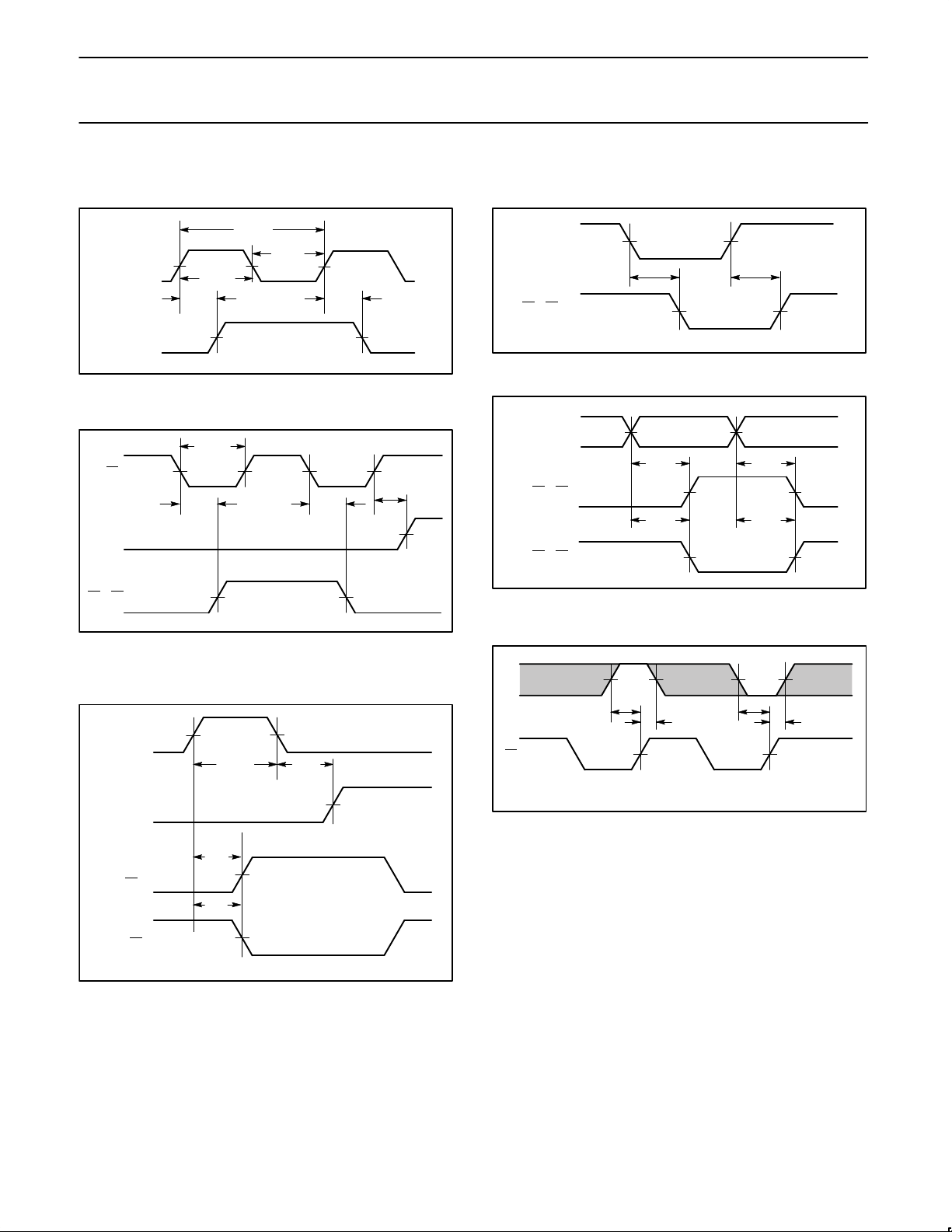
AC WAVEFORMS
For all waveforms Vm = 1.5V
V
M
t
PLH
t
PHL
V
M
V
M
V
M
CPU, CP
D
Qn
1/f
MAX
tW(L)
SF00750
tW(H)
t
rec
V
M
V
M
V
M
PL
tW(L)
V
M
VMV
M
t
PLH
t
PHL
CPU, CP
D
V
M
TCU, TCD, Qn
SF00751
V
M
V
M
V
M
V
M
t
PLH
MR
tW(H) t
rec
V
M
t
PHL
CPU, CP
D
Qn, TC
D
TC
U
SF00752
V
M
V
M
V
M
V
M
t
PLH
t
PHL
CPU, CP
D
TCU, TC
D
SF00753
V
M
V
M
V
M
t
PHL
t
PLH
V
M
t
PHL
t
PLH
V
M
V
M
Dn
Qn
,
TCU, TC
D
Qn
,
TC
U
, TC
D
SF00754
V
M
V
M
Dn
PL
tS(H)
th(H)
tS(L)
th(L)
V
M
SF00755
The shaded areas indicate when the input is permitted to change
for predictable output performance.
Waveform 2. Propagation Delay, Clock to Terminal Count
Waveform 1. Propagation Delay, Clock Input to Output,
Clock Pulse Width and Maximum Clock Frequency
Waveform 3. Parallel Pulse Width,
Parallel Load to Output Delays, and Parallel Load
to Clock Recovery Time
Waveform 5. Master Reset Pulse Width, Master Reset to Output
Delay and Master Reset to Clock Recovery Time
Waveform 4. Propagation Delay, Data to Flip-Flop Outputs,
Terminal Count Up and Down Outputs
Waveform 6. Data Setup and Hold Times
Page 7
Philips Semiconductors Product specification
74F193Up/down binary counter with separate up/down clocks
1995 Jul 17
7
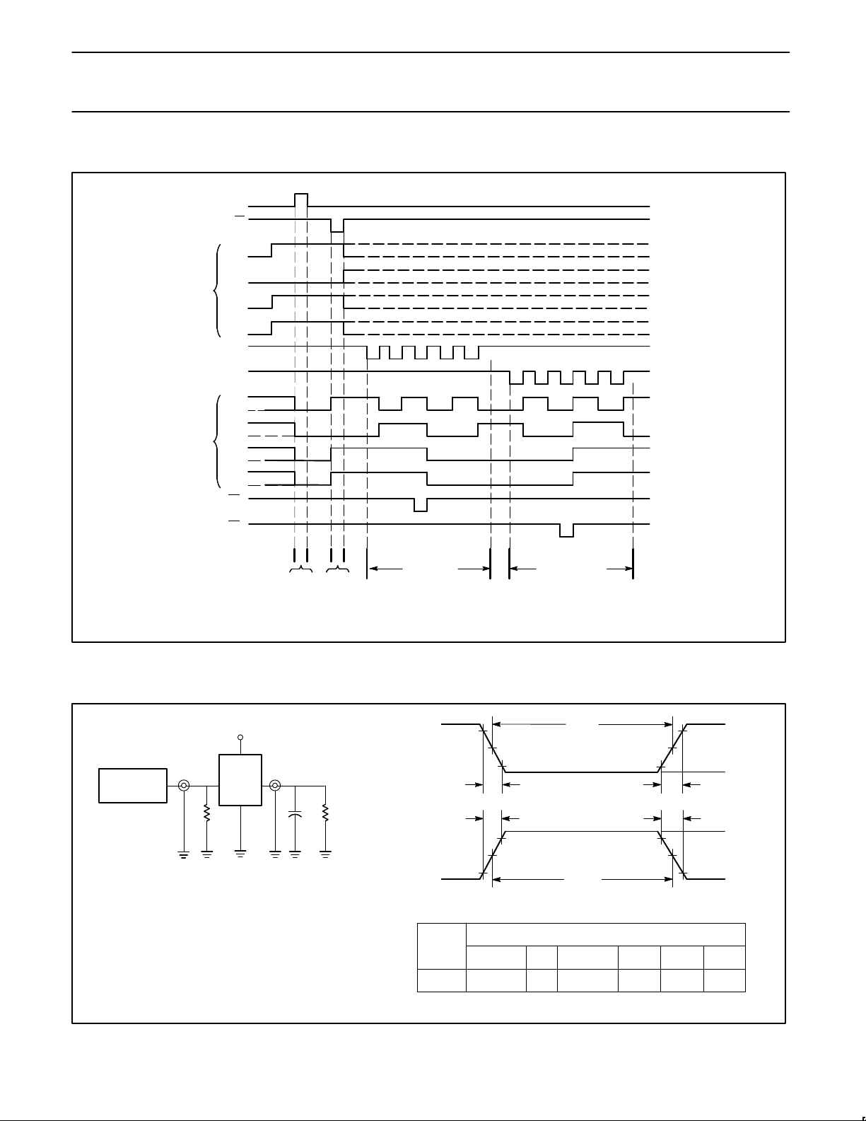
Timing Diagram (Typical clear, load, and count sequence)
NOTES:
1. Clear overrides load, data, and count inputs.
2. When counting up, count-down input must be High; when counting down, count-up input must be High.
Q0
Q1
Q2
Q3
0 13 14 15 0 1 2 1 0 15 14 13
COUNT UP COUNT DOWN
CLEAR PRESET
CLEAR
1
LOAD
D0
D1
D2
D3
COUNT UP
2
COUNT DOWN
2
SEQUENCE
DATA
OUTPUTS
MR
PL
CP
U
CP
D
TC
U
TC
D
SF00756
Binary Counter
TEST CIRCUIT AND WAVEFORMS
t
w
90%
V
M
10%
90%
V
M
10%
90%
V
M
10%
90%
V
M
10%
NEGATIVE
PULSE
POSITIVE
PULSE
t
w
AMP (V)
0V
0V
t
THL (tf
)
INPUT PULSE REQUIREMENTS
rep. rate
t
w
t
TLHtTHL
1MHz 500ns
2.5ns 2.5ns
Input Pulse Definition
V
CC
family
74F
D.U.T.
PULSE
GENERATOR
R
L
C
L
R
T
V
IN
V
OUT
Test Circuit for Totem-Pole Outputs
DEFINITIONS:
R
L
= Load resistor;
see AC ELECTRICAL CHARACTERISTICS for value.
C
L
= Load capacitance includes jig and probe capacitance;
see AC ELECTRICAL CHARACTERISTICS for value.
R
T
= Termination resistance should be equal to Z
OUT
of
pulse generators.
t
THL (tf
)
t
TLH (tr
)
t
TLH (tr
)
AMP (V)
amplitude
3.0V
1.5V
V
M
SF00006
 Loading...