

Page 1

INTEGRATED CIRCUITS
74F198
8-bit bidirectional universal shift register
Product specification
IC15 Data Handbook
1987 Oct 02
Page 2
Philips Semiconductors Product specification
74F1988-bit bidirectional universal shift register
FEA TURES
•Buffered clock and control inputs
•Shift right, shift left, and parallel load capability
•Asynchronous Master Reset
DESCRIPTION
The 74F198 Bidirectional Universal Shift Register is designed to
incorporate virtually all of the features a system designer may want
in a shift register. This circuit features parallel inputs and outputs,
shift right and shift left serial inputs, operating mode select inputs,
and direct overriding master reset input. The register has four
distinct modes of operation:
– Parallel (broadside) load
– Shift right (in the direction Q0 toward Q7)
– Shift left (in the direction Q7 toward Q0)
– Inhibit clock (do nothing).
Synchronous parallel loading is accomplished by applying the 8 bits
of data and taking both mode control inputs, S0 and S1, High. The
data is loaded into the associated flip-flop and appears at the
outputs after the positive transition of the clock inputs. During
loading, serial data flow is inhibited.
Shift right is accomplished synchronously, with the rising edge of the
clock pulse when S0 is High and S1 is Low. Serial data for this
mode is entered at the right data input (D
S1 is High, data shifts left synchronously and new data is entered at
the shift-left serial input (D
SL
).
Clocking of the flip-flops is inhibited when both mode control inputs
are Low.
). When S0 is Low and
SR
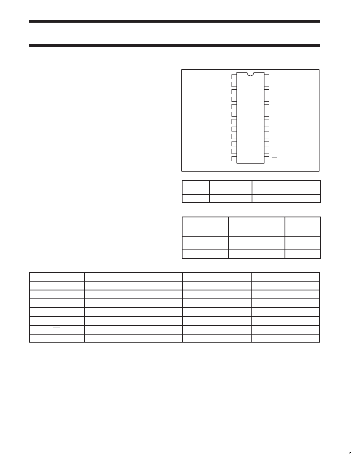
PIN CONFIGURATION
1
S0
2
D
SR
3
D0
4
Q0
5
D1
6
Q1
7
D2
8
Q2
9
D3
10
Q3
11
CP
12 13
GND
TYPE TYPICAL f
TYPICAL SUPPL Y CURRENT
MAX
74F198 95MHz 73mA
24
23
22
21
20
19
18
17
16
15
14
SF00160
V
CC
S1
D
SL
D7
Q7
D6
Q6
D5
Q5
D4
Q4
MR
(TOTAL)
ORDERING INFORMATION
COMMERCIAL RANGE
DESCRIPTION
24-pin Plastic Slim
DIP (300mil)
24-pin Plastic SOL N74F198D SOT137-1
VCC = 5V ±10%,
T
= 0°C to +70°C
amb
N74F198N SOT222-1
PKG DWG #
INPUT AND OUTPUT LOADING AND FAN-OUT TABLE
PINS DESCRIPTION 74F (U.L.) HIGH/LOW LOAD VALUE HIGH/LOW
D0–D7 Parallel data inputs 1.0/1.0 20µA/0.6mA
D
SR
D
SL
S0–S1 Mode Select inputs 1.0/1.0 20µA/0.6mA
CP Clock Pulse input (Active rising edge) 1.0/1.0 20µA/0.6mA
MR Master Reset input (Active Low) 1.0/1.0 20µA/0.6mA
Q0–Q7 Data outputs 50/33 1.0mA/20mA
NOTE: One (1.0) FAST unit load is defined as: 20µA in the High state and 0.6mA in the Low state.
Serial data input (Shift Right) 1.0/1.0 20µA/0.6mA
Serial data input (Shift Left) 1.0/1.0 20µA/0.6mA
October 2, 1987 853–0089 90746
2
Page 3
Philips Semiconductors Product specification
MR
CP
Q0
Q1…Q6
Q7
74F1988-bit bidirectional universal shift register
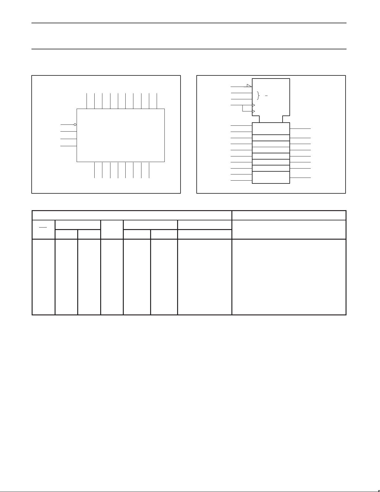
LOGIC SYMBOL
13
1
23
11
= Pin 24
V
CC
GND = Pin 12
79
35
222
D1 D2
D3D0
MR
S0
S1
CP
D
SR
Q0 Q1 Q2 Q3
46810
19 21
15 17
D5 D6
Q5 Q6 Q7
Q4
14 16 18 20
D7D4
D
SF00161
SL
IEC/IEEE SYMBOL
13
1
23
11
2
3
5
7
9
15
17
19
21
22
R
0
M
1
C4
1 → /2 ←
1, 4D
3, 4D
3, 4D
3, 4D
2, 4D
SRG8
0
3
4
6
8
10
14
16
18
20
SF00162
FUNCTION TABLE
INPUTS OUTPUTS
MODE
S0 S1
L X X X X X X L L L L
H X X L X X X Q00 Q10 Q60 Q70
H H H ↑ X X 0…7 0 167
H H L ↑ X H X H Q0n Q5n Q6n
H H L ↑ X L X L Q0n Q5n Q6n
H L H ↑ H X X Q1n Q2n Q7n H
H L H ↑ L X X Q1n Q2n Q7n L
H L L X X X X Q00 Q10 Q60 Q70
H = High voltage level
L = Low voltage level
X = Don’t care
↑ = Low-to-High transition of designated input
0…7 = The level of steady input at inputs 0 through 7, respectively.
Q00, Q10, Q60, Q70 = The level of Q0, Q1, Q6, Q7, respectively, before the indicated steady state input conditions were established.
Q0n, Q1n, Q6n, Q7n = The level of Q0, Q1, Q6, Q7, respectively, before the most recent Low-to-High clock transition.
SERIAL PARALLEL
LEFT RIGHT 0…7
October 2, 1987
3
Page 4
Philips Semiconductors Product specification
74F1988-bit bidirectional universal shift register
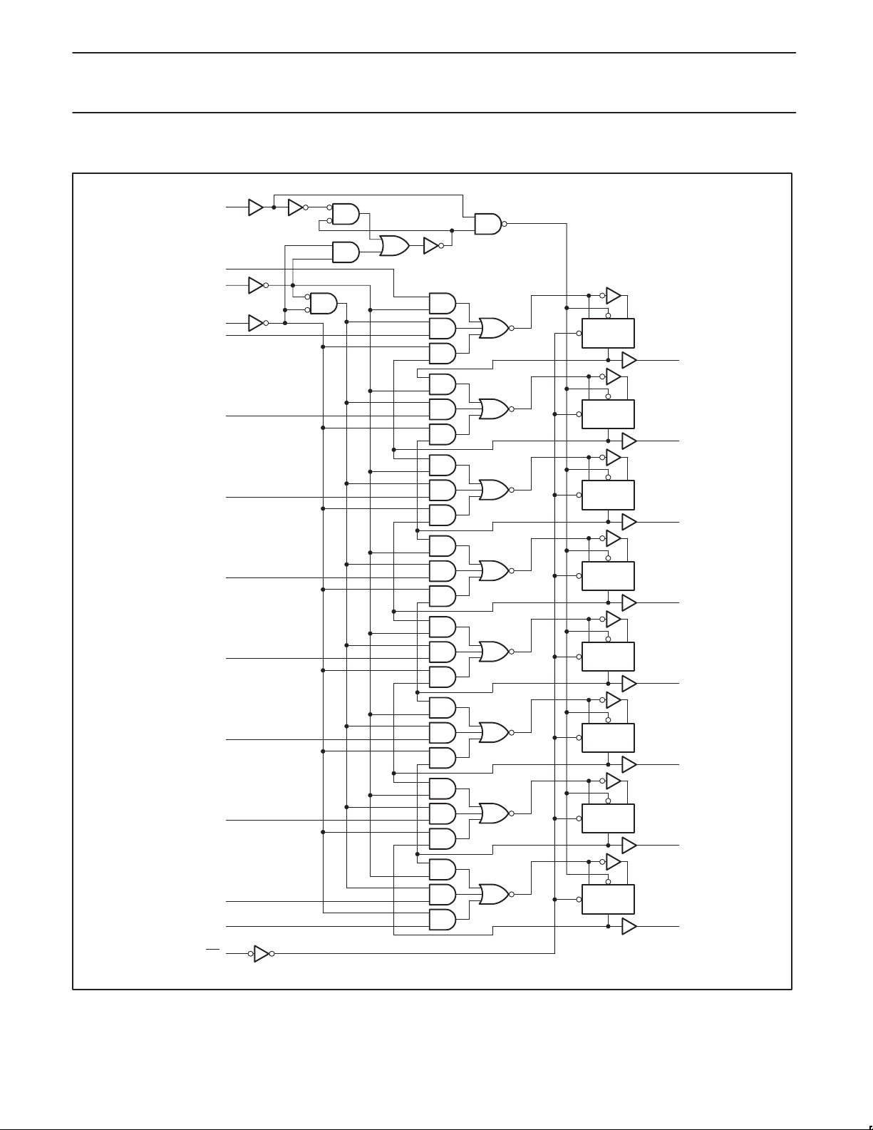
LOGIC DIAGRAM
11
CP
2
D
SR
23
S1
1
S0
3
D0
RCPS
Q
4
Q0
5
D1
7
D2
9
D3
15
D4
17
D5
19
D6
RCPS
Q
RCPS
Q
RCPS
Q
RCPS
Q
RCPS
Q
RCPS
Q
6
Q1
8
Q2
10
Q3
14
Q4
16
Q5
18
Q6
October 2, 1987
D
MR
21
D7
22
SL
13
RCPS
Q
20
SF00163
Q7
4
Page 5

Philips Semiconductors Product specification
SYMBOL
PARAMETER
UNIT
74F1988-bit bidirectional universal shift register
TYPCIAL TIMING DIAGRAM
CP
S0
S1
MR
SERIAL
DATA
INPUTS
PARALLEL
DATA
INPUTS
OUTPUTS
BIT A
L
H
H
L
H
L
H
L
H
H
LL
HH
HH
HHHHH
CLEAR LOAD
LLL
SHIFT RIGHT
BIT A
ABSOLUTE MAXIMUM RATINGS
(Operation beyond the limits set forth in this table may impair the useful life of the device.
Unless otherwise noted these limits are over the operating free-air temperature range.)
SYMBOL
V
CC
V
IN
I
IN
V
OUT
I
OUT
T
amb
T
stg
Supply voltage –0.5 to +7.0 V
Input voltage –0.5 to +7.0 V
Input current –30 to +5 mA
Voltage applied to output in High output state –0.5 to V
Current applied to output in Low output state 40 mA
Operating free-air temperature range 0 to +70 °C
Storage temperature range –65 to +150 °C
PARAMETER RATING UNIT
RECOMMENDED OPERATING CONDITIONS
V
V
V
I
I
I
T
CC
IH
IL
IK
OH
OL
amb
Supply voltage 4.5 5.0 5.5 V
High-level input voltage 2.0 V
Low-level input voltage 0.8 V
Input clamp current –18 mA
High-level output current –1 mA
Low-level output current 20 mA
Operating free-air temperature range 0 +70 °C
SHIFT LEFT
LIMITS
MIN NOM MAX
INHIBIT
CC
CLEAR
SF00165
V
October 2, 1987
5
Page 6

Philips Semiconductors Product specification
SYMBOL
PARAMETER
TEST CONDITIONS
1
UNIT
VOHHigh-level output voltage
V
VOLLow-level output voltage
V
ICCSupply current (total)
V
MAX
74F1988-bit bidirectional universal shift register
DC ELECTRICAL CHARACTERISTICS
(Over recommended operating free-air temperature range unless otherwise noted.)
LIMITS
MIN TYP
p
p
V
IK
I
I
I
IH
I
IL
I
OS
Input clamp voltage VCC = MIN, II = I
Input current at maximum input voltage VCC = MAX, VI = 7.0V 100 µA
High-level input current VCC = MAX, VI = 2.7V 20 µA
Low-level input current VCC = MAX, VI = 0.5V –0.6 mA
Short-circuit output current
pp
3
I
CCH
I
CCL
VCC = MIN, VIL = MAX ±10%V
VIH = MIN, IOH = MAX ±5%V
CC
VCC = MIN, VIL = MAX ±10%V
VIH = MIN, IOL = MAX ±5%V
IK
CC
VCC = MAX –60 –150 mA
=
CC
CC
CC
2.5
2.7 3.4
NOTES:
1. For conditions shown as MIN or MAX, use the appropriate value specified under recommended operating conditions for the applicable type.
2. All typical values are at V
3. Not more than one output should be shorted at a time. For testing I
CC
= 5V, T
techniques are preferable in order to minimize internal heating and more accurately reflect operational values. Otherwise, prolonged shorting
amb
= 25°C.
, the use of high-speed test apparatus and/or sample-and-hold
OS
of a High output may raise the chip temperature well above normal and thereby cause invalid readings in other parameter tests. In any
sequence of parameter tests, I
tests should be performed last.
OS
2
MAX
0.35 0.50
0.35 0.50
–0.73 –1.2 V
70 100 mA
75 110 mA
October 2, 1987
6
Page 7

Philips Semiconductors Product specification
74F1988-bit bidirectional universal shift register
AC ELECTRICAL CHARACTERISTICS
LIMITS
SYMBOL PARAMETER
TEST
CONDITION
VCC = +5.0V
T
= +25°C
amb
C
= 50pF, RL = 500Ω
L
MIN TYP MAX MIN MAX
f
MAX
t
PLH
t
PHL
t
PHL
Maximum clock frequency Waveform 1 80 95 70 MHz
Propagation delay
CP to Qn
Waveform 1
5.0
6.0
7.5
8.5
10.0
11.0
Propagation delay Waveform 3 5.0 7.5 10.0 4.5 11.0 ns
AC SETUP REQUIREMENTS
SYMBOL PARAMETER
tS(H)
tS((L)
th(H)
th(L)
tS(H)
tS(L)
th(H)
th(L)
tS(H)
tS(L)
th(H)
th(L)
tw(H)
tw(L)
Setup time, High or Low
Dn to CP
Hold time, High or Low
Dn to CP
Setup time, High or Low
DSR, DSL to CP
Hold time, High or Low
DSR, DSL to CP
Setup time, High or Low
Sn to CP
Hold time, High or Low
Sn to CP
CP Pulse width,
High or Low
TEST
CONDITION
Waveform 2
Waveform 2
Waveform 2
Waveform 2
Waveform 2
Waveform 2
Waveform 1
tw(L) MR Pulse width, Low Waveform 3 5.0 5.0 ns
t
REC
Recovery time MR to CP Waveform 3 5.0 6.0 ns
VCC = +5.0V
T
= +25°C
amb
C
= 50pF, RL = 500Ω
L
MIN TYP MAX MIN MAX
0.0
3.0
0.0
3.5
0.0
3.0
0.0
2.5
9.0
6.0
0.0
0.0
5.0
5.0
VCC = +5.0V ± 10%
T
amb
C
= 50pF, RL = 500Ω
L
4.5
5.5
LIMITS
VCC = +5.0V ± 10%
T
amb
C
= 50pF, RL = 500Ω
L
0.0
3.0
1.0
4.0
0.0
3.0
0.0
3.0
10.0
7.0
0.0
0.0
6.0
6.0
= 0°C to +70°C
11.0
12.0
= 0°C to +70°C
UNIT
ns
UNIT
ns
ns
ns
ns
ns
ns
ns
October 2, 1987
7
Page 8

Philips Semiconductors Product specification
74F1988-bit bidirectional universal shift register
AC WAVEFORMS
For all waveforms, VM = 1.5V.
The shaded areas indicate when the input is permitted to change for predictable output performance.
1/f
MAX
tw(L)
CP
Qn
V
M
tw(H)
t
PHL
V
M
t
PLH
V
M
V
M
SF00166
Waveform 1. Propagation ’Delay, Clock Input to Output,
Clock Widths, and Maximum Clock Frequency
MR
CP
Qn
V
M
tw(L)
t
PHL
V
M
V
M
t
REC
V
M
SF00158
Waveform 3. Master Reset Pulse Width, Master Reset to
Output Delay and Master Reset to Clock Recovery Time
Dn, Sn
DSR, D
CP
V
SL
M
ts(H)
V
M
th(H)
V
M
Waveform 2. Setup Time and Hold Time
V
ts(L)
V
M
M
th(L)
V
M
SF00164
TEST CIRCUIT AND WAVEFORMS
V
CC
V
PULSE
GENERATOR
IN
R
T
Test Circuit for Totem-Pole Outputs
DEFINITIONS:
R
= Load resistor;
L
see AC ELECTRICAL CHARACTERISTICS for value.
= Load capacitance includes jig and probe capacitance;
C
L
see AC ELECTRICAL CHARACTERISTICS for value.
R
= Termination resistance should be equal to Z
T
pulse generators.
D.U.T.
V
OUT
C
t
NEGATIVE
PULSE
R
L
L
POSITIVE
PULSE
90%
10%
V
M
10%
t
THL (tf
t
TLH (tr
90%
V
M
w
V
M
10%
)
)
t
w
t
TLH (tr
t
THL (tf
)
)
90%
V
M
90%
10%
AMP (V)
0V
AMP (V)
0V
Input Pulse Definition
INPUT PULSE REQUIREMENTS
V
amplitude
3.0V
M
1.5V
rep. rate
1MHz 500ns
t
w
t
TLHtTHL
2.5ns 2.5ns
SF00006
OUT
of
family
74F
October 2, 1987
8
Page 9

Philips Semiconductors Product specification
8-bit bidirectional universal shift register
DIP24: plastic dual in-line package; 24 leads (300 mil) SOT222-1
74F198
1987 Oct 02
9
Page 10

Philips Semiconductors Product specification
8-bit bidirectional universal shift register
SO24: plastic small outline package; 24 leads; body width 7.5 mm SOT137-1
74F198
1987 Oct 02
10
Page 11

Philips Semiconductors Product specification
8-bit bidirectional universal shift register
NOTES
74F198
1987 Oct 02
11
Page 12

Philips Semiconductors Product specification
8-bit bidirectional universal shift register
Data sheet status
Data sheet
status
Objective
specification
Preliminary
specification
Product
specification
Product
status
Development
Qualification
Production
Definition
This data sheet contains the design target or goal specifications for product development.
Specification may change in any manner without notice.
This data sheet contains preliminary data, and supplementary data will be published at a later date.
Philips Semiconductors reserves the right to make chages at any time without notice in order to
improve design and supply the best possible product.
This data sheet contains final specifications. Philips Semiconductors reserves the right to make
changes at any time without notice in order to improve design and supply the best possible product.
[1]
74F198
[1] Please consult the most recently issued datasheet before initiating or completing a design.
Definitions
Short-form specification — The data in a short-form specification is extracted from a full data sheet with the same type number and title. For
detailed information see the relevant data sheet or data handbook.
Limiting values definition — Limiting values given are in accordance with the Absolute Maximum Rating System (IEC 134). Stress above one
or more of the limiting values may cause permanent damage to the device. These are stress ratings only and operation of the device at these or
at any other conditions above those given in the Characteristics sections of the specification is not implied. Exposure to limiting values for extended
periods may affect device reliability.
Application information — Applications that are described herein for any of these products are for illustrative purposes only. Philips
Semiconductors make no representation or warranty that such applications will be suitable for the specified use without further testing or
modification.
Disclaimers
Life support — These products are not designed for use in life support appliances, devices or systems where malfunction of these products can
reasonably be expected to result in personal injury . Philips Semiconductors customers using or selling these products for use in such applications
do so at their own risk and agree to fully indemnify Philips Semiconductors for any damages resulting from such application.
Right to make changes — Philips Semiconductors reserves the right to make changes, without notice, in the products, including circuits, standard
cells, and/or software, described or contained herein in order to improve design and/or performance. Philips Semiconductors assumes no
responsibility or liability for the use of any of these products, conveys no license or title under any patent, copyright, or mask work right to these
products, and makes no representations or warranties that these products are free from patent, copyright, or mask work right infringement, unless
otherwise specified.
Philips Semiconductors
811 East Arques Avenue
P.O. Box 3409
Sunnyvale, California 94088–3409
Telephone 800-234-7381
Copyright Philips Electronics North America Corporation 1998
All rights reserved. Printed in U.S.A.
print code Date of release: 10-98
Document order number: 9397-750-05097
yyyy mmm dd
12
 Loading...