

Datasheet N74ALS245A-1D, N74ALS245A-1DB, N74ALS245A-1N, N74ALS245AD, N74ALS245ADB Datasheet (Philips)
...Page 1

74ALS245A/74ALS245A–1
Octal transceiver (3–State)
Product specification
IC05 Data Handbook
1991 Jun 03
INTEGRATED CIRCUITS
Page 2
Philips Semiconductors Product specification
74ALS245A/74ALS245A-1Octal transceiver (3-State)
2
1991 Jun 03 853–001 1 02709
FEA TURES
•Octal bidirectional bus interface
•3-State buffer outputs sink 24mA and source 15mA
•Outputs are placed in high impedance state during power-off
conditions
•The -1 version sinks 48mA
DESCRIPTION
The 74ALS245A is an octal transceiver featuring non-inverting
3-State bus compatible outputs in both transmit and receive
directions. The device features an output enable (OE
) input for easy
cascading and transmit/receive (R/T
) input for direction control.
The 74ALS245A-1 is the same as the 74ALS245A except that both
ports sink 48mA within the ±5% V
CC
range.
TYPE
TYPICAL
PROPAGATION
DELA Y
TYPICAL
SUPPLY CURRENT
(TOTAL)
74ALS245A 7.0ns 34mA
74ALS245A-1 7.0ns 34mA
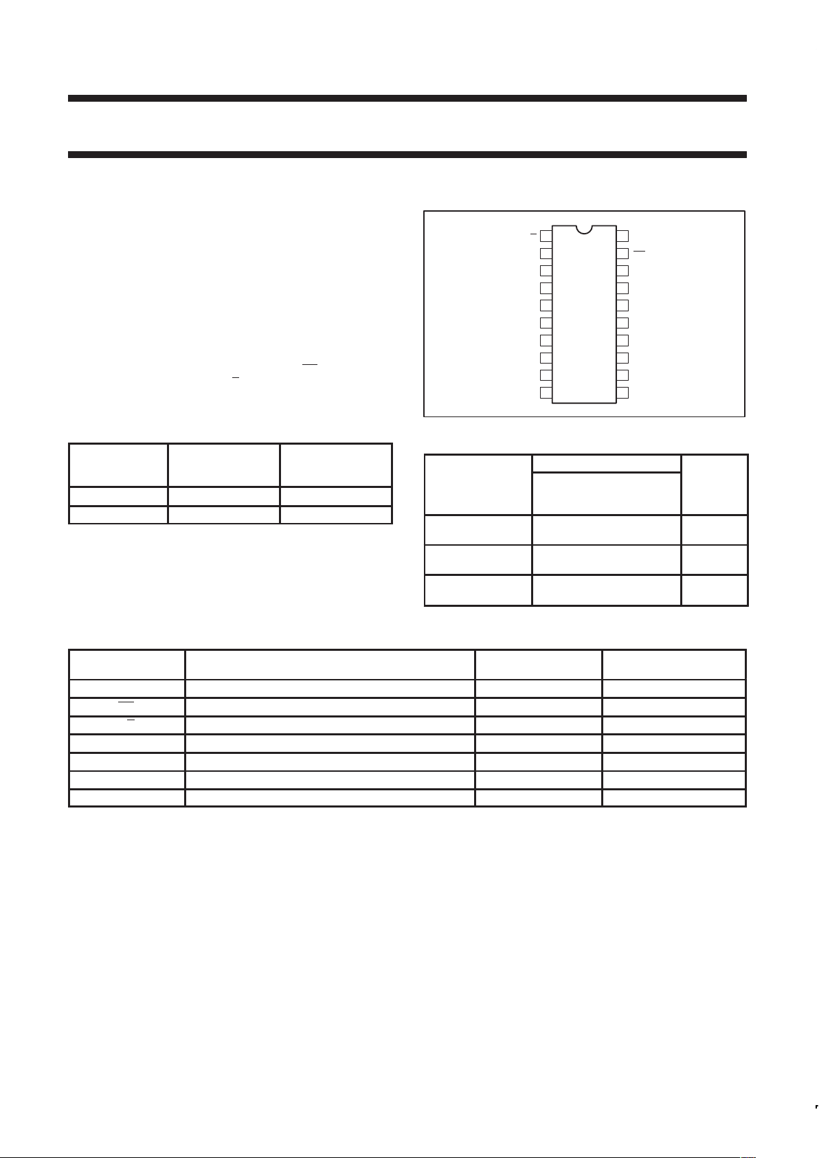
PIN CONFIGURATION
SF00198
1
2
3
4
5
6
7
8
9
10 11
12
13
14
15
16
17
18
19
20
T/R
A0
A1
A2
A3
A4
A5
A6
A7
GND
V
CC
OE
B0
B1
B2
B3
B4
B6
B5
B7
ORDERING INFORMA TION
ORDER CODE
DESCRIPTION
COMMERCIAL RANGE
V
CC
= 5V ±10%,
T
amb
= 0°C to +70°C
DRAWING
NUMBER
20-pin plastic DIP
74ALS245AN,
74ALS245A-1N
SOT146-1
20-pin plastic SOL
74ALS245AD,
744ALS245A-1D
SOT163-1
20-pin plastic SSOP
Type II
74ALS245ADB,
74ALS245A-1DB
SOT339-1
INPUT AND OUTPUT LOADING AND FAN-OUT TABLE
PINS DESCRIPTION
74ALS (U.L.)
HIGH/LOW
LOAD VALUE
HIGH/LOW
A0 – A7, B0 – B7 Data inputs 1.0/1.0 20µA/0.1mA
OE Output Enable input (active-Low) 1.0/1.0 20µA/0.1mA
T/R T ransmit/receive input 1.0/1.0 20µA/0.1mA
A0 – A7 A port outputs 750/240 15mA/24mA
B0 – B7 B port outputs 750/240 15mA/24mA
A0 – A7 A port outputs (-1 version) 750/480 15mA/48mA
B0 – B7 B port outputs (-1 version) 750/480 15mA/48mA
NOTE: One (1.0) ALS unit load is defined as: 20µA in the High state and 0.1mA in the Low state.
Page 3
Philips Semiconductors Product specification
74ALS245A/74ALS245A-1Octal transceiver (3-State)
1991 Jun 03
3
LOGIC SYMBOL
B2 B3 B4 B5
16 15 14 13
234
V
CC
= Pin 20
GND = Pin 10
SF00199
B1
17
B0
18
19
1
OE
T/R
A0 A1 A2 A3 A4 A5
567
B6 B7
12 11
A6 A7
89
IEC/IEEE SYMBOL
SC00097
G3
19
3EN1 [BA]
1
3EN2 [AB]
∇ 1
2 ∇
2
3
4
5
6
7
8
9
18
17
16
15
14
13
12
11
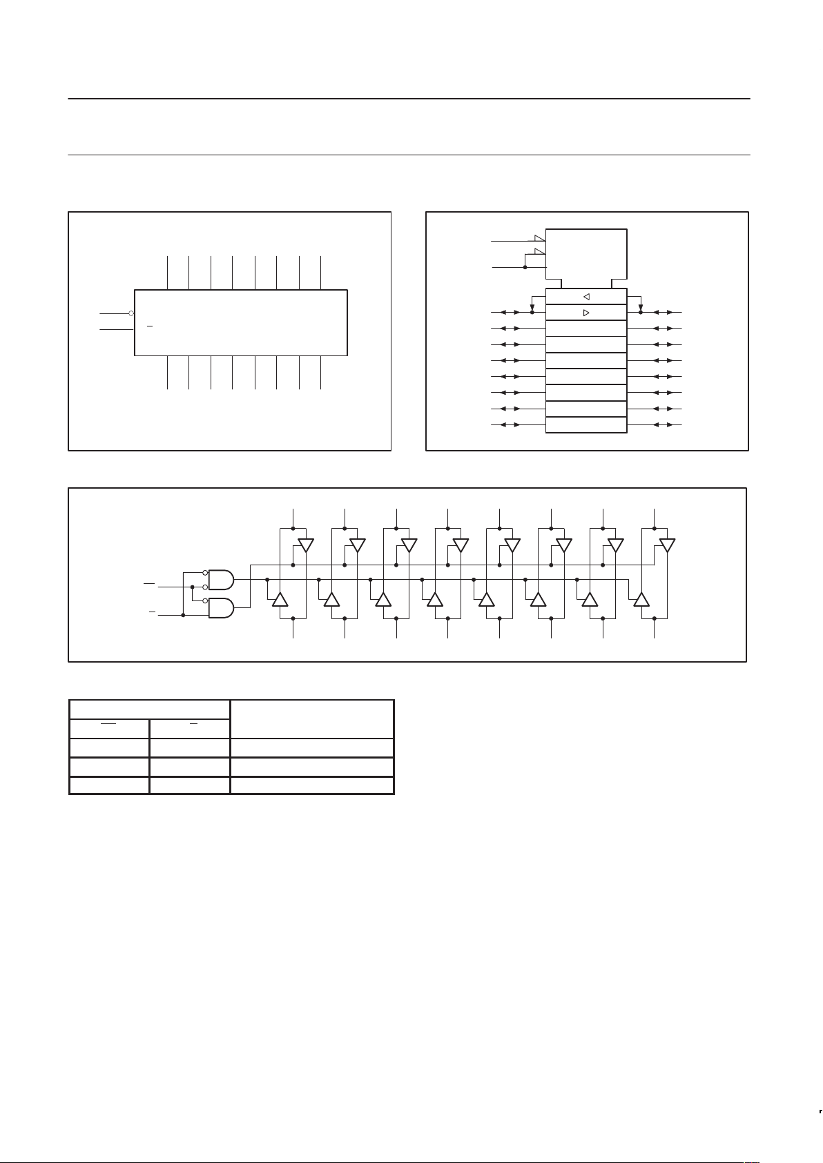
LOGIC DIAGRAM
SF00201
18
B0
17
B1
16
B2
15
B3
14
B4
13
B5
12
B6
11
B7
A0 A1 A2 A3 A4 A5 A6 A7
23456789
19
1
OE
T/R
VCC = Pin 20
GND = Pin 10
FUNCTION TABLE
INPUTS
OE T/R
OUTPUTS
L L Bus B data to Bus A
L H Bus A data to Bus B
H X Z
H = High voltage level
L = Low voltage level
X = Don’t care
Z = High impedance “off” state
Page 4

Philips Semiconductors Product specification
74ALS245A/74ALS245A-1Octal transceiver (3-State)
1991 Jun 03
4
ABSOLUTE MAXIMUM RATINGS
(Operation beyond the limit set forth in this table may impair the useful life of the device.
Unless otherwise noted these limits are over the operating free air temperature range.)
SYMBOL
PARAMETER RATING UNIT
V
CC
Supply voltage –0.5 to +7.0 V
V
IN
Input voltage –0.5 to +7.0 V
I
IN
Input current –30 to +5 mA
V
OUT
Voltage applied to output in High output state –0.5 to V
CC
V
pp
p
p
All versions 48 mA
I
OUT
Current applied to output in Low output state
-1 version 96 mA
T
amb
Operating free-air temperature range 0 to +70 °C
T
stg
Storage temperature range –65 to +150 °C
RECOMMENDED OPERATING CONDITIONS
LIMITS
SYMBOL
PARAMETER
MIN NOM MAX
UNIT
V
CC
Supply voltage 4.5 5.0 5.5 V
V
IH
High-level input voltage 2.0 V
V
IL
Low-level input voltage 0.8 V
I
IK
Input clamp current –18 mA
I
OH
High-level output current –15 mA
p
All versions 24 mA
IOLLow-level output current
-1 version 48
1
mA
T
amb
Operating free-air temperature range
0 +70 °C
NOTES:
1. The 48mA limit applies only under the condition of V
CC
= 5.0V ± 5%.
Page 5

Philips Semiconductors Product specification
74ALS245A/74ALS245A-1Octal transceiver (3-State)
1991 Jun 03
5
DC ELECTRICAL CHARACTERISTICS
(Over recommended operating free-air temperature range unless otherwise noted.)
LIMITS
SYMBOL
PARAMETER
TEST CONDITIONS
1
MIN TYP
2
MAX
UNIT
VCC±10%, VIL = MAX,
IOH = –0.4mA V
CC
– 2 V
-
p
CC
,
IL
,
VIH = MIN
IOH = –3mA 2.4 3.2 V
VOHHigh level out ut voltage
VCC = MIN, VIL = MAX,
V
IH
= MIN
IOH = –15mA 2.0 V
VCC = MIN, VIL = MAX,
I
OL
= 12mA 0.25 0.40 V
-
p
All versions
CC
,
IL
,
VIH = MIN
I
OL
= 24mA 0.35 0.50 V
VOLLow level out ut voltage
-1 version
VCC = 4.75V , VIL = MAX,
V
IH
= MIN
I
OL
= 48mA 0.35 0.50 V
V
IK
Input clamp voltage VCC = MIN, II = I
IK
–0.73 –1.5 V
Input current at maxi-
OE or T/R VCC = MAX, VI = 7.0V 0.1 mA
I
I
mum input voltage
A or B ports VCC = MAX, VI = 5.5V 0.1 mA
I
IH
High-level input current
3
VCC = MAX, VI = 2.7V 20 µA
I
IL
Low-level input current
3
VCC = MAX, VI = 0.4V –0.1 mA
I
O
Output current
4
VCC = MAX, VO = 2.25V –30 –112 mA
I
CCH
28 45 mA
I
CC
Supply current (total)
I
CCL
VCC = MAX
40 55 mA
I
CCZ
44 58 mA
NOTES:
1. For conditions shown as MIN or MAX, use the appropriate value specified under recommended operating conditions for the applicable type.
2. All typical values are at V
CC
= 5V, T
amb
= 25°C.
3. For I/O ports, the parameter I
IH
and IIL include the off-state current.
4. The output conditions have been chosen to produce a current that closely approximates one half of the true short-circuit output current, I
OS
.
AC ELECTRICAL CHARACTERISTICS
LIMITS
SYMBOL PARAMETER TEST CONDITION
T
amb
= 0°C to +70°C
V
CC
= +5.0V ± 10%
C
L
= 50pF, RL = 500Ω
UNIT
MIN MAX
t
PLH
t
PHL
Propagation delay
An to Bn, Bn to An
Waveform 1
2.0
2.0
10.0
10.0
ns
t
PZH
t
PZL
Output enable time
to High or Low level
Waveform 2
Waveform 3
3.0
3.0
20.0
20.0
ns
t
PHZ
t
PLZ
Output disable time
from High or Low level
Waveform 2
Waveform 3
2.0
4.0
10.0
15.0
ns
Page 6

Philips Semiconductors Product specification
74ALS245A/74ALS245A-1Octal transceiver (3-State)
1991 Jun 03
6
AC WAVEFORMS
For all waveforms, VM = 1.3V .
V
M
V
M
V
M
V
M
t
PHL
t
PLH
An, Bn
Bn, An
SC00096
Waveform 1. Propagation Delay for Non-inverting Outputs
V
M
V
M
V
M
t
PHZ
t
PZH
OE
An, Bn
VOH -0.3V
0V
SC00094
Waveform 2. 3-State Output Enable Time to High Level
and Output Disable Time from High Level
V
M
V
M
V
M
t
PLZ
t
PZL
OE
An, Bn
V
OL
+0.3V
SC00095
3.5V
Waveform 3. 3-State Output Enable Time to Low Level
and Output Disable Time from Low Level
TEST CIRCUIT AND WAVEFORMS
t
w
90%
V
M
10%
90%
V
M
10%
90%
V
M
10%
90%
V
M
10%
NEGATIVE
PULSE
POSITIVE
PULSE
t
w
AMP (V)
0.3V
0.3V
t
THL (tf
f
)
INPUT PULSE REQUIREMENTS
Rep.Rate
t
w
t
TLHtTHL
1MHz
500ns
2.0ns 2.0ns
Input Pulse Definition
V
CC
Family
74ALS
D.U.T.
PULSE
GENERATOR
R
L
C
L
R
T
V
IN
V
OUT
Test Circuit for 3-State Outputs
DEFINITIONS:
R
L
= Load resistor;
see AC electrical characteristics for value.
C
L
= Load capacitance includes jig and probe capacitance;
see AC electrical characteristics for value.
R
T
= Termination resistance should be equal to Z
OUT
of
pulse generators.
t
THL (tf
)
t
TLH (tr
)
t
TLH (tr
)
AMP (V)
Amplitude
3.5V
1.3V
V
M
SC00072
R
L
7.0V
SWITCH POSITION
TEST SWITCH
t
PLZ
, t
PZL
closed
All other open
Page 7

Philips Semiconductors Product specification
74ALS245A/74ALS245A–1Octal transceiver (3–State)
1991 Jun 03
7
DIP20: plastic dual in-line package; 20 leads (300 mil) SOT146-1
Page 8

Philips Semiconductors Product specification
74ALS245A/74ALS245A–1Octal transceiver (3–State)
1991 Jun 03
8
SO20: plastic small outline package; 20 leads; body width 7.5 mm SOT163-1
Page 9

Philips Semiconductors Product specification
74ALS245A/74ALS245A–1Octal transceiver (3–State)
1991 Jun 03
9
SSOP20: plastic shrink small outline package; 20 leads; body width 5.3 mm SOT339-1
Page 10

Philips Semiconductors Product specification
74ALS245A/74ALS245A–1Octal transceiver (3–State)
1991 Jun 03
10
Philips Semiconductors and Philips Electronics North America Corporation reserve the right to make changes, without notice, in the products,
including circuits, standard cells, and/or software, described or contained herein in order to improve design and/or performance. Philips
Semiconductors assumes no responsibility or liability for the use of any of these products, conveys no license or title under any patent, copyright,
or mask work right to these products, and makes no representations or warranties that these products are free from patent, copyright, or mask
work right infringement, unless otherwise specified. Applications that are described herein for any of these products are for illustrative purposes
only. Philips Semiconductors makes no representation or warranty that such applications will be suitable for the specified use without further testing
or modification.
LIFE SUPPORT APPLICA TIONS
Philips Semiconductors and Philips Electronics North America Corporation Products are not designed for use in life support appliances, devices,
or systems where malfunction of a Philips Semiconductors and Philips Electronics North America Corporation Product can reasonably be expected
to result in a personal injury. Philips Semiconductors and Philips Electronics North America Corporation customers using or selling Philips
Semiconductors and Philips Electronics North America Corporation Products for use in such applications do so at their own risk and agree to fully
indemnify Philips Semiconductors and Philips Electronics North America Corporation for any damages resulting from such improper use or sale.
This data sheet contains preliminary data, and supplementary data will be published at a later date. Philips
Semiconductors reserves the right to make changes at any time without notice in order to improve design
and supply the best possible product.
Philips Semiconductors
811 East Arques Avenue
P.O. Box 3409
Sunnyvale, California 94088–3409
Telephone 800-234-7381
DEFINITIONS
Data Sheet Identification Product Status Definition
Objective Specification
Preliminary Specification
Product Specification
Formative or in Design
Preproduction Product
Full Production
This data sheet contains the design target or goal specifications for product development. Specifications
may change in any manner without notice.
This data sheet contains Final Specifications. Philips Semiconductors reserves the right to make changes
at any time without notice, in order to improve design and supply the best possible product.
Copyright Philips Electronics North America Corporation 1997
All rights reserved. Printed in U.S.A.
 Loading...