

Datasheet MXL1001ACJ8, MXL1001ACN8, MXL1001ACS8, MXL1001AMH, MXL1001AMJ8 Datasheet (Maxim)
...Page 1
19-0286; Rev 1; 8/94
Precision Operational Amplifier
_______________General Description
The MXL1001 offers significant specification improvement
over earlier precision operational amplifiers and is pincompatible with the industry-standard LT1001. Particular
attention has been paid to the optimization of key parameters such as input offset voltage, common-mode rejection,
and power-supply rejection. In addition, the high-performance MXL1001C commercial temperature device provides considerable cost savings when compared to
equivalent grades of competing precision amplifiers.
The input offset voltage of all units is less than 60µV,
allowing the premium military device, the MXL1001AM, to
be specified at 15µV max. Power dissipation is close to
half that of the industry-standard OP-07 precision op
amp, without sacrificing noise or speed performance. A
useful by-product of lower dissipation is decreased
warm-up drift.
________________________Applications
Thermocouple Amplifiers
Low-Level Signal Processing
Strain Gauge Amplifiers
High-Accuracy Data Acquisition
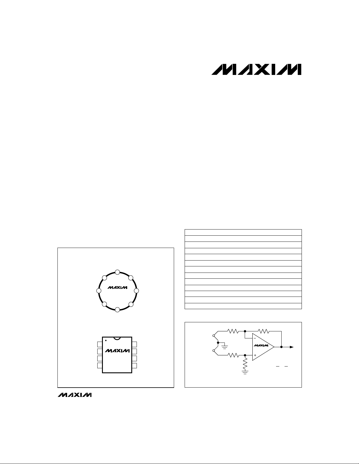
__________________Pin Configuration
TOP VIEW
V
TRIM
OS
8
V
TRIM
OS
1 7
-IN
TRIM
V
OS
-IN
+IN
V-
MXL1001
3
+IN
TO-99
1
2
MXL1001
3
4
DIP/SO
V+
62
V
OUT
5
N.C.
4
V-
8
TRIM
V
OS
7
V+
6
V
OUT
5
N.C.
____________________________Features
♦ Guaranteed Low Offset Voltage
MXL1001AM: 15µV max
MXL1001C: 60µV max
♦ Guaranteed Low Drift
MXL1001AM: 0.6µV/°C max
MXL1001C: 1.0µV/°C max
♦ Guaranteed Low Bias Current
MXL1001AM: 2nA max
MXL1001C: 4nA max
♦ Guaranteed CMRR
MXL1001AM: 114dB min
MXL1001C: 110dB min
♦ Guaranteed PSRR
MXL1001AM: 110dB min
MXL1001C: 106dB min
♦ Low Power Dissipation
MXL1001AM: 75mW max
MXL1001C: 80mW max
♦ Low Noise: 0.3µV
p-p
______________Ordering Information
PART
MXL1001ACN8
MXL1001CN8
MXL1001ACS8 0°C to +70°C
MXL1001CS8
MXL1001ACJ8 0°C to +70°C
MXL1001CJ8
MXL1001ACH 0°C to +70°C
MXL1001CH
MXL1001AMJ8 -55°C to +125°C
MXL1001MJ8 -55°C to +125°C 8 CERDIP
MXL1001AMH
MXL1001MH -55°C to +125°C
TEMP. RANGE PIN-PACKAGE
0°C to +70°C
0°C to +70°C
0°C to +70°C 8 SO
0°C to +70°C 8 CERDIP
0°C to +70°C 8 TO-99
-55°C to +125°C 8 TO-99
8 Plastic DIP
8 Plastic DIP
8 SO
8 CERDIP
8 TO-99
8 CERDIP
8 TO-99
__________Typical Operating Circuit
SENSING
JUNCTION
REFERENCE
JUNCTION
R1
R2
R4
HIGH-STABILITY
THERMOCOUPLER AMPLIFIER
R3
MXL1001
R1R3R2
=
R4
MXL1001
________________________________________________________________
Maxim Integrated Products
Call toll free 1-800-998-8800 for free samples or literature.
1
Page 2
Precision Operational Amplifier
ABSOLUTE MAXIMUM RATINGS
Total Supply Voltage (V+ to V-) ...........................................±22V
Continuous Power Dissipation .........................................500mW
TO-99(H)—derate at 7.1mW/°C above +80°C
CERDIP(J)—derate at 6.7mW/°C above +75°C
Plastic DIP(P)—derate at 5.6mW/°C above +36°C
Small Outline(S)—derate at 5mW/°C above +55°C
Differential Input Voltage .....................................................±30V
Input Voltage (Note 1)..........................................................±22V
MXL1001
Note 1: For supply voltages less than ±22V, the absolute maximum input voltage is equal to the supply voltage.
Stresses beyond those listed under “Absolute Maximum Ratings” may cause permanent damage to the device. These are stress ratings only, and functional
operation of the device at these or any other conditions beyond those indicated in the operational sections of the specifications is not implied. Exposure to
absolute maximum rating conditions for extended periods may affect device reliability.
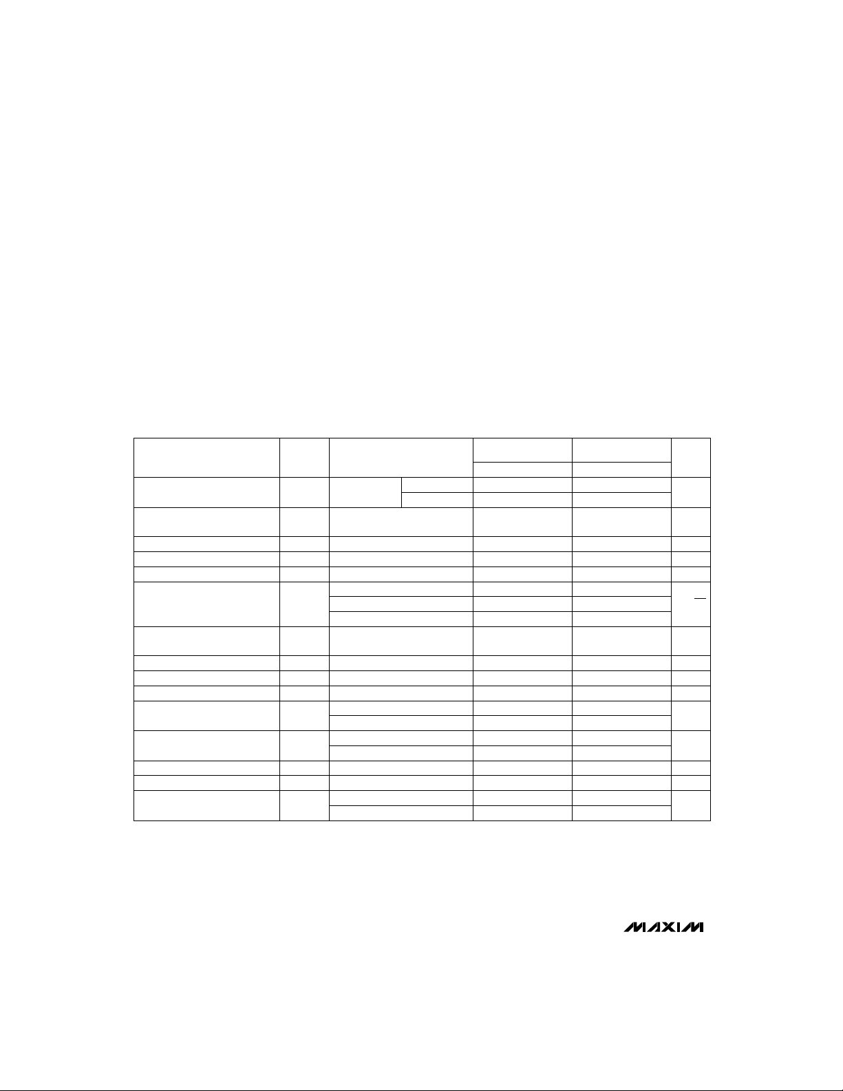
ELECTRICAL CHARACTERISTICS
(VS= ±15V, TA= +25°C, unless otherwise noted.)
SYMBOLPARAMETER
Input Offset Voltage
Long-Term Input Offset
Voltage Stability
Input Offset Current
Input Bias Current
Input Noise Voltage
Input Noise Voltage Density 10.0 13.0
Input Resistance
(Differential Mode)
Large-Signal Voltage Gain
Output Voltage Swing
Power Consumption
Note 2: MXL1001A grade VOSis measured one minute after application of power. For all other grades VOSis measured
approximately 0.5 seconds after application of power.
Note 3: Long-Term Input Offset Voltage Stability refers to the average trend line of V
30 days of operation. Excluding the initial hour of operation, changes in V
2.5µV. Parameter is sample tested.
Note 4: Sample tested.
Note 5: Guaranteed by design.
V
OS
OS
B
N p-p
e
N
IN
A
VO
V
O
P
D
CONDITIONS
(Note 2)
(Note 3)
0.1Hz to 10Hz (Note 4)
fO= 10Hz (Note 4)
fO= 100Hz (Note 4)
fO= 1000Hz (Note 4)
(Note 5)
VCM= ±13V
VS= ±3V to ±18V
RL≥ 2kΩ, VO= ±12V
RL≥ 1kΩ, VO= ±10V
RL≥ 2kΩ
RL≥ 1kΩ
RL≥ 2kΩ (Note 4)
A
= +1V (Note 4)
VCL
VS= ±15V, no load
VS= ±3V, no load
Duration of Output Short Circuit ....................................Indefinite
Operating Temperature Ranges:
MXL1001C_/AC_.................................................0°C to +70°C
MXL1001M_/AM_...........................................-55°C to +125°C
Junction Temperature (T
Storage Temperature Range.............................-65°C to +150°C
Lead Temperature (soldering, 10sec).............................+300°C
MXL1001AM
MXL1001AC
MIN TYP MAX
MXL1001AM
MXL1001AC
450 800
300 500
±13.0 ±14.0
±12.0 ±13.5
OS
during the first 30 operating days are typically
OS
).................................-65°C to +160°C
J
MXL1001M
MXL1001C
MIN TYP MAX
715
10 25
0.2 1.0VOS/Time
0.3 0.6e
10.3 18.0
9.6 11.0
46 75
46
vs. Time over extended periods after the first
18 60
18 60
0.3 1.5
0.4 3.8
±0.7 ±4.0
0.3 0.6
10.5 18.0
10.0 13.0
9.8 11.0
15 80
±13 ±14
110 126
106 123
400 800
250 500
±13.0 ±14.0
±12.0 ±13.5
0.1 0.25
0.4 0.8
48 80
48
UNITS
µV
µV/
Month
nA0.3 2.0I
nA±0.5 ±2.0I
µV
p-p
nV/√Hz
MΩ30 100R
V±13 ±14IVRInput Voltage Range
dB114 126CMRRCommon-Mode Rejection Ratio
dB110 123PSRRPower-Supply Rejection Ratio
V/mV
V
V/µs0.1 0.25SRSlew Rate
MHz0.4 0.8BWClosed-Loop Bandwidth
mW
2 _______________________________________________________________________________________
Page 3

Precision Operational Amplifier
ELECTRICAL CHARACTERISTICS
(VS= ±15V, -55°C ≤ TA≤ +125°C, unless otherwise noted.)
SYMBOLPARAMETER
Input Offset Voltage
Average Temperature Coefficient
of Input Offset Voltage
Input Offset Current
Input Bias Current
Large-Signal Voltage Gain
Output Voltage Swing V
Power Dissipation P
CONDITIONS
(Note 6)
OS
OS
OS
B
VCM= ±13V
VS= ±3V to ±18V
RL≥ 2kΩ, VO= ±10V
VO
RL≥ 2kΩ ±12.5 ±13.5 ±12.5 ±13.5 V
O
No load 55 90 60 100 mW
D
MXL1001AM
MIN TYP MAX
MXL1001M
MIN TYP MAX
45 160
0.3 1.0
1.2 7.6
±1.5 ±8.0
±13 ±14
106 120
100 117
200 700
UNITS
µV/°C0.2 0.6TCV
V/mV300 700A
ELECTRICAL CHARACTERISTICS
(VS= ±15V, 0°C ≤ TA≤ +70°C, unless otherwise noted.)
SYMBOLPARAMETER
Input Offset Voltage
Average Temperature Coefficient
of Input Offset Voltage
Input Offset Current
Input Bias Current
Large-Signal Voltage Gain
Output Voltage Swing V
Power Dissipation
Note 6: MXL1001A grade offset voltage is measured one minute after application of power. For all other grades VOSis measured
0.5 seconds after power on.
OS
P
OS
OS
B
VO
O
D
CONDITIONS
(Note 6)
VCM= ±13V
VS= ±3V to ±18V
RL≥ 2kΩ, VO= ±10V
RL≥ 2kΩ ±12.5 ±13.8 ±12.5 ±13.8 V
No load 50 85 55 90 mW
MXL1001AC
MIN TYP MAX
MXL1001C
MIN TYP MAX
30 110
0.3 1.0
0.6 5.3
±1.0 ±5.5
±13 ±14
106 123
103 120
250 750
UNITS
µV/°C0.2 0.6TCV
V/mV350 750A
MXL1001
µV30 60V
nA0.8 4.0I
nA±1.0 ±4.0I
V±13 ±14IVRInput Voltage Range
dB110 122CMRRCommon-Mode Rejection Ratio
dB104 117PSRRPower-Supply Rejection Ratio
µV20 60V
nA0.5 3.5I
nA±0.7 ±3.5I
V±13 ±14IVRInput Voltage Range
dB110 124CMRRCommon-Mode Rejection Ratio
dB106 120PSRRPower-Supply Rejection Ratio
_______________________________________________________________________________________ 3
Page 4

Precision Operational Amplifier
__________Applications Information
The MXL1001 series devices are pin-compatible with the
OP-07, OP-05, 725, 108A or 101A amplifiers. The
MXL1001 amplifiers can be used to upgrade older
designs using these devices, with or without removal of
external frequency compensation or nulling components.
The MXL1001 can also be used in 741, LF156 or OP-15
applications provided the nulling circuitry is removed.
MXL1001
The MXL1001 is specified over a wide supply voltage
range from ±3V to ±18V. Operation with lower supplies
is possible down to ±1.2V (two NiCd batteries), however, at this level the device is stable only in closed-loop
gains of +2 and above (or inverting gain of one or higher). Unless proper care is exercised, thermocouple
effects caused by temperature gradients across dissimilar metals at the input terminal connections, can exceed
the inherent offset-voltage drift of the amplifier. Air currents over the device leads should be minimized, package leads should be short, and the two input leads
should be as close together as possible and maintained
at the same temperature.
Offset-Voltage Adjustment
The input offset voltage of the MXL1001, and its temperature drift, are minimized by zener-zap trimming at the
wafer level. If further nulling of VOSis required, this can
be performed using a 10kΩ or 20kΩ potentiometer with
no degradation of VOSdrift with temperature. Trimming
to a value other than zero creates a drift of
(VOS/300)µV/°C; i.e., if VOSis adjusted to 300µV, the
change in drift will be 1µV/°C. The adjustment range
with a 10kΩ or 20kΩ potentiometer is approximately
±2.5mV. If less adjustment range is needed, the sensitivity and resolution of the offset nulling can be improved
by using a potentiometer of lower ohmic value in conjunction with fixed resistors.
Figure 1. Optional Offset Nulling Circuit
___________________Chip Topography
V
OS
VOS TRIM -IN
SUBSTRATE IS CONNECTED TO V-
20k
1
INPUT
TRIM VOS TRIM V+
2
3
0.102"
(2.59mm)
8
MXL1001
4
V-
+IN
V+
7
6
OUTPUT
V
OUT
0.076"
(1.93mm)
V-
Maxim cannot assume responsibility for use of any circuitry other than circuitry entirely embodied in a Maxim product. No circuit patent licenses are
implied. Maxim reserves the right to change the circuitry and specifications without notice at any time.
4
___________________Maxim Integrated Products, 120 San Gabriel Drive, Sunnyvale, CA 94086 (408) 737-7600
© 1994 Maxim Integrated Products Printed USA is a registered trademark of Maxim Integrated Products.
 Loading...