

Page 1
1
www.clare.com
MXED101
DS-MXED101-R9
The MXED101 is a 6-bit, 192-output column driver IC
designed to drive passive matrix full-color (RGB) and monochrome Organic Light Emitting Diode (OLED) displays. Each
of the 192 current outputs is designed to act as a precision
high impedance current source. The MXED101 current source
output supply range is from 15 to 30V. The outputs are
arranged in a row on one side of the die with a pitch of 92
microns, which facilitates easy interface with the display.
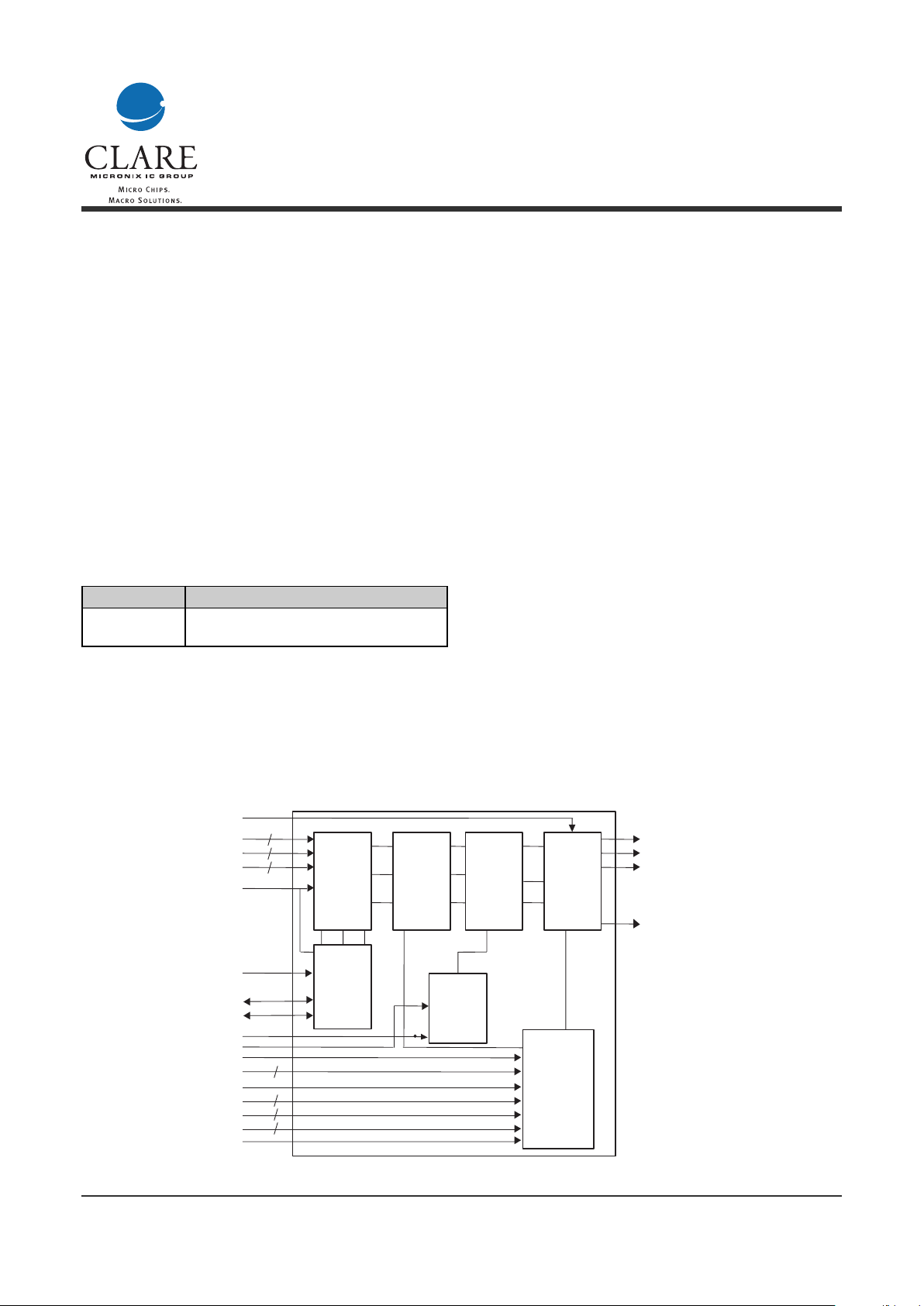
The MXED101 consists of an Input Register, Transfer Latch,
Comparator, Bi-directional Shift Register, Counter, and 192
Programmable Current Outputs. The device has three 6-bit
input data buses, DA(5-0), DB(5-0), and DC(5-0), to accept
RGB or monochrome data. This data can be clocked through
the device at a maximum speed of 55 MHz with a 5V logic supply (40 MHz with a 3.3V logic supply).
The outputs of the MXED101 are arranged in three programmable interdigitized banks (A, B, and C) of 64 outputs each, a
bank for each color of the RGB data (programming the output
current is described in the Functional Description section). Bank
A controls outputs 1, 4, 7, …, 190; Bank B controls outputs 2, 5,
8, …, 191; and Bank C controls outputs 3, 6, 9, …, 192.
The MXED101 employs three methods to adjust display brightness: a global gain voltage, a 3-bit digital control for each color,
and an external 10.8 KW resistor. In addition to these methods,
the relative brightness of each output can be controlled by onchip pulse width modulation. A standby signal (STBY) is provided to place the display in low power standby mode whenever it
is necessary.
• CMOS technology
• 192 Precision outputs
• Programmable output current control
• Optimized adjacent channel and chip-to-chip output
matching
• 3.3V or 5V logic supply voltage
• 55 MHz clock frequency
• Cascadable
• 30V output driver supply voltage
• Bi-directional data transfer
• Supports Grayscale, Binary, and Standby modes
• Low power consumption
• Package type: TCP (MXED101TP) and Die
(MXED101DI)
Features:
General Description
30V, 192-Channel OLED Display Driver
Ordering Information
Part # Description
MXED101 30V, 192-Channel OLED
Display Driver
Block Diagram
Q1
Q2
Q3
.
.
.
Q192
.
.
.
.
192 X 6
Input
Register
192 x 6
Transfer
Latch
192 x 6
Comparator
Program-
mable
192-
channel
Output
Terminal
64 x 1
Bi-
Direction
Shift
Register
6-Bit
Up
Counter
Output
Mapping/
Current
Programmin
g
SWC
DA(5-0)
DB(5-0)
DC(5-0)
CLKSH
DIRTKN
RTKNB
LTKNB
LE
CLKEX
STBY
SDM(1-0)
GG
GA(2-0)
GB(2-0)
GC(2-0)
RG
Q1
Q2
Q3
Q192
Page 2
www.clare.com
MXED101
Rev. 9
Electrical Characteristics
Absolute Maximum Ratings are stress ratings. Stresses
in excess of these ratings can cause permanent damage to the device. Functional operation of the device at
these or any other conditions beyond those indicated in
the operational sections of this data sheet is not implied.
Exposure of the device to the absolute maximum ratings for an extended period may degrade the device
and effect its reliability.
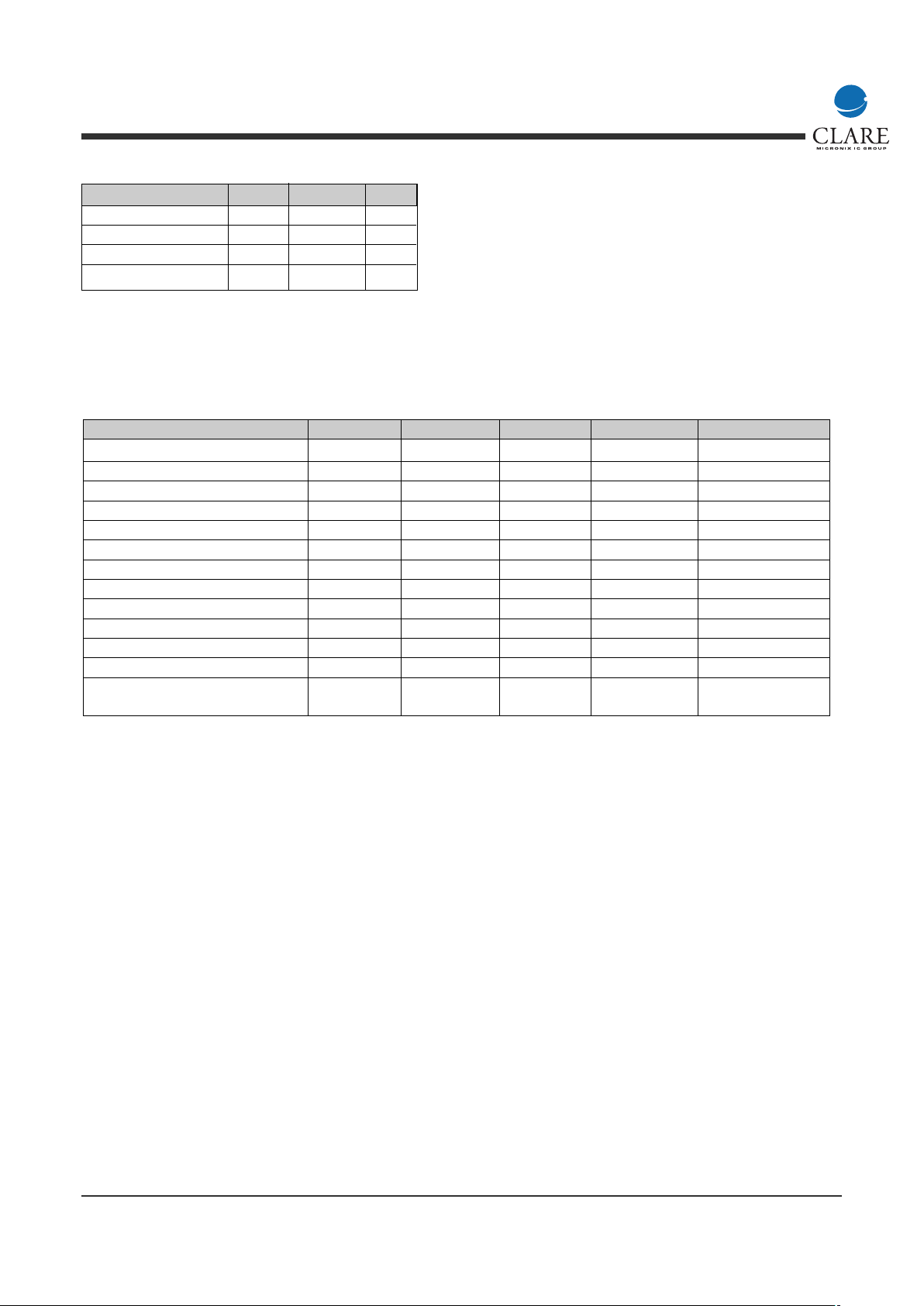
Absolute Maximum Ratings (Vss=OV)
2
Parameter Symbol Rating Unit
Logic Supply Voltage V
CC
-0.3 to 7.0 Vdc
Analog Supply Voltage V
DD
-.3 to 35.0 Vdc
Logic Input Voltage V
LIN
-.3 to VCC+.3 Vdc
Storage Temperature T
STG
-55 to 125 ˚C
Parameter Symbol Test Conditions Min Max Units
Logic Supply Voltage V
CC
3.0 5.5 Vdc
Analog Supply Voltage V
DD
15 30 Vdc
GG Voltage V
GG
VDD≥ 15V 0 12 Vdc
External RGPin Resistor R
RG
-0.1% +0.1% 10.8KΩ
High Logic Input Level V
IH
Vcc - 0.6 Vcc + 0.2 Vdc
Low Logic Input Level V
IL
-0.2 .6 Vdc
High Logic Level Input Current I
IH
-10 10 µA
Low Logic Level Input Current I
IL
-10 10 µA
High Logic Output Level V
OH
IOH>-10µA Vcc-0.2 V
Low Logic Output Level V
OL
IOL<10µA 0.2 V
Logic Supply Current I
cc
7mA
Analog Supply Current** I
DD
6.0 + Iout mA
Operating Temperature T
J
20 100 ˚C
(Junction)
**Analog supply current is highly dependable on the output current of the 192 output channels (Iout), which is determined by the application.
Note: V
dout
, I
bank
, and I
die
are transferred to the output parameters channels table.
Page 3
MXED101
www.clare.com
Rev. 9
3
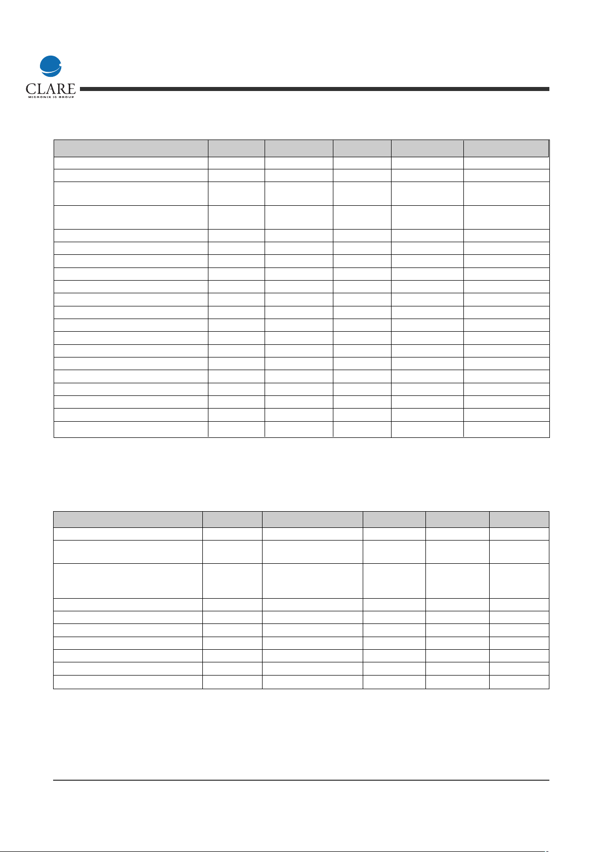
Digital Timing for Vcc in Range of 4.5 to 5.5 VDC
Parameter Symbol Min Typ Max Units
Shift Clock Frequency (VCC=4.5 + 5.5V) f
CLK
55 MHz
Shift Clock Frequency (VCC=3.0 to 4.4V) 40 MHz
Shift Clock Frequency Pulse Width t
SPW
722 nS
(VCC=4.5 + 5.5V)
Shift Clock Frequency Pulse Width t
SPW
9.6 30 nS
(VCC=3.0 to 4.4V)
Shift Clock Frequency Duty Cycle DC
SCK
40 50 60 %
Shift Clock to Latch Delay t
DSKL
3 (clock Cycles) nS
Exposure Clock Frequency f
EKF
10 MHz
Exposure Clock Pulse Width t
EPW
40 500 nS
Exposure Duty Cycle DC
EX
40 50 60 %
Data Setup Time t
DSU
5— — nS
Data Hold Time t
DHD
5— — nS
Token Setup Time t
TSU
5— — nS
Token Hold Time t
tHD
5— — nS
Token Bit Output Delay t
STD
—— 13 nS
Token Bit Pulse Width t
TPW
15 — — nS
Latch Pulse Width t
LAPW
50 — — nS
Last data to Latch Enable Time t
DLD
200 — — nS
Latch Disable to Exposure Clock Time t
LED
50 — — nS
Exposure Clock to Latch Enable Time t
DLE
50 — — nS
Standby to Ready Time t
STBY
10 mS
Output Channel Parameters
Parameter Symbol Typ Min Max Units
Driver Output Voltage Compliance V
Qn
VDD-3 Vdc
Per bank max to min channel output O<V
Qn<VDD
- 3,
current ratio I
BANK
V
Qn
match to 2V 1.0 1.04 A/A
High output die to low output die O<V
Qn<VDD
- 3,
average output current ratio I
DIE
V
Qn
match to 2V 1.0 1.02 A/A
R
RG
match to 0.1%
Output Current Rise Time t
IOR
_ _ 200 nS
Output Current Fall Time t
IOF
_ _ 200 nS
Output Current Settling Time t
IOS
_ _ 350 nS
Exposure Clock to Output High Delay t
OHD
_ _ 220 nS
Exposure Clock to Output Low Delay t
OLD
_ _ 220 nS
Channel output current rise/fall time t
IORF
10% to 90% 250 nS
Shorting Switch Resistance V(Qn) = IV 800 Ω
Page 4

www.clare.com
4
MXED101
Rev. 9
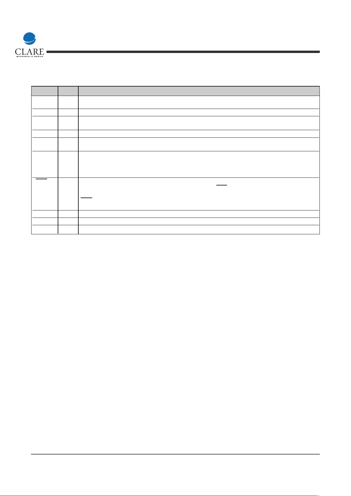
Signal Definition
Name I/0/A Description
V
DD
Power supply for the 192 current driver output channels - 6 pads
V
CC
Low voltage logic power supply - 2 pads
GND Ground - 4 pads
ISHRT Ground used to short the 192 current driver output channels - 4 pads. Note: There can be high currents on this line.
It should be seperated from the circuit ground pads (GND) to prevent ground bounce.
RSTB I Reset: Active low signal used to reset digital logic for test purposes. This input is pulled high internally.
CLKSH I Token Shift Clock: Used to shift tokens down the length of the driver IC. The direction of token shift is
determined by DIRTKN pin. It is possible to load only a portion of the 192 output channels prior to latching in
applications not requiring the full 192 channels. The speed of the clock is from DC to 55 MHz at 5V logic power
supply (40 MHz at 3.3V).
LTKNB I/O Left Token Bit: Used to pass the tokens into and out of the driver IC. The pin is used as input for shift right and as
output for shift left. High state represents the presence of token. The shifting is performed from DC to 55 MHz
(40 MHz at 3.3V).
RTKNB I/O Right Token Bit: Used to pass the tokens into and out of the driver IC. The pin is used as input for shift left and as
output for shift right. High state represents the presence of token. The shifting is performed from DC to 55 MHz
(40 MHz at 3.3V).
DIRTKN I Token Direction: Used to determine the shift direction of the token. When the signal is high, causes the token to shift
left to right (1–>64) and when the signal is low causes the token to shift to left (64–>1). This input is pulled high
internally. The token shifts 3 cells at a time to account for the 3 parallel data inputs.
LE I Latch Enable: Active high signal used to latch RGB data from the driver outputs into a set of transfer latches. Once a
line of data is latched into the transfer latch, OLED exposure can begin. At the same time, a new line of exposure data
can be loaded into the input register of the driver IC. On the rising edge of the of LE, all token registers are cleared, the
exposure counter is asynchronously preset to a low state and exposure data is allowed to pass from the input register
to the transfer latch. On the falling edge of LE, the exposure counter and output drivers are enabled within t
LED
(50 ns).
DA(5-0) I 6-bit Data input A. Signal bus used for the exposure data input word for outputs 1,4,7,…,190. The driver performs
at clock speed from DC to 55 MHz (40 MHz at 3.3V).
DB(5-0) I 6-bit Data input B. Signal bus used for the exposure data input word for outputs 2,5,8,…,191. The driver performs
at clock speed from DC to 55 MHz (40 MHz at 3.3V).
DC(5-0) I 6-bit Data input C. Signal bus used for the exposure data input word for channels 3,6,9,…,192. The driver performs
at clock speed from DC to 55 MHz (40 MHz at 3.3V).
CLKEX I Exposure Clock: Signal (DC to 10 MHz signal) used to clock the input of the driver ICs exposure counter (6-bits).
The signal is used to cycle the driver IC internal counter from 0 up to 63. The signal must be cycled at least 64 times
between LE pulses to completely cycle the counter. The first rising edge of CLKEX will enable all non zero outputs with-
out changing the counter. Additional rising edges of CLKEX will increment the counter. When the counter and data of
values for an output match, the output is disabled until LE re-enables the exposure counter. Cycles of CLKEX beyond 64
will have no effect until the next cycle of LE re-enables the counter.
TGR I Binary/Grayscale: Signal used to determine if the driver IC is either 6 bit grayscale or binary. Low –> grayscale.
High –> Binary. This input is internally pulled to a logic low.
GG A Global Gain: Used to set the global current gain. The voltage range on this pin is 0V to 12V when V
DD
is ≥ 15V. The
base current level is GG/RG, with a peak base current level of 1.455mA. This input is internally pulled to a logic low.
Page 5
MXED101
www.clare.com
5
Rev. 9
Signal Definition (continued)
Name I/0/A Description
RG A Resistor Gain: Used to set the global current gain. A precision resistor shall be connected from this node to
analog ground which, in conjunction with the GG input voltage, sets up the base current level of the chip.
GA(2-0) I A Gain: Used to set the current on driver output channels 1,4,7,…,190. This input is internally pulled to a logic low.
GB(2-0) I B Gain: Used to set the current on driver output channels 2,5,8,…,191. This input is internally pulled to a
logic low.
GC(2-0) I C Gain: Used to set the current on driver output channels 3,6,9,…,192. This input is internally pulled to a logic low.
STBY I Standby Reset: Active high signal used to place the IC in a low power standby mode. When in the high state the IC
is non-functional and power dissipation is minimized. This input is internally pulled to a logic low.
SDM(1-O) I Stripe/Diagonal/Mosaic: These input signals are used to modify the output channel current levels depending on
which row of the display is active. The falling edge of LE is used to modify the A, B, C channels. When the STBY is
set to a logic high, the A, B, C channel outputs are reset to their initial mapping. These inputs are internally pulled to
a logic high. (See the SDM function below).
SWC I Switch Channels: This input signal is used to control when the individual output channels are in the tri-state condition
(current is not sourced and the switch to ground is off). When the SWC input is in the high state, each output
channel turns the switch to ground on as soon as the data count is matched and current source disabled. When
SWC is in the low state, each channel remains in the tri-state condition from when the current source is disabled
until the counter equals 63. This input is internally pulled to a logic low.
TST(9-0) I These pins should be left open circuited.
TEST(2-0) A These pins should be left open circuited.
Q1-Q192 A OLED current source driver outputs.
Note: A= > analog, I= > digital input, O= > digital output
Page 6
www.clare.com
6
MXED101
Rev. 9
Functional Description
Output Current Hold-On-Time Control
There are two modes for controlling the 192 outputs current hold-on-times:
1- Grayscale: The grayscale is obtained when the TGR pin is low or open. Each of the three banks has a 6-bit con-
trol word, DA(5-0), DB(5-0), and DC(5-0), that is updated at the CLKSH signal clock which allows each output to
turn on for a period of 0 to 63 counts of the CLKEX signal clock.
2- Binary Mode: Binary mode is obtained when the TGR input signal is high. Data is loaded in a similar way that is
described in the grayscale mode. After the data is latched the DA5, DB5, or DC5 data bit is gated with CLKEX to
determine the on or off status of the output drivers.
Output Current Magnitude Control
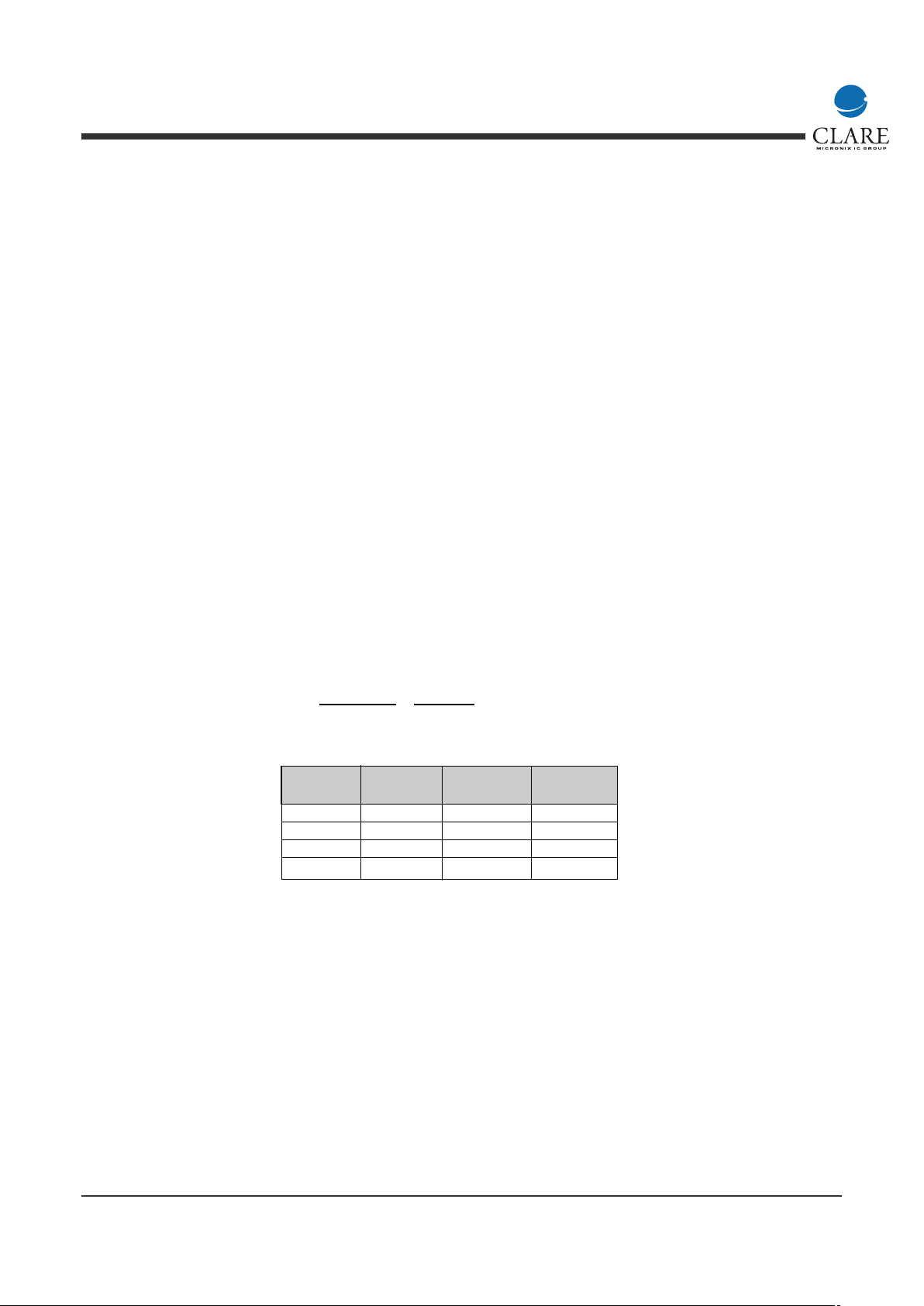
GG, RG, GA(2-0), GB(2-0), and GC(2-0) controls the output current of the output drivers in the three banks. A precision 10.8 KΩ (+/- 0.1%) resistor is tied from RG to ground. A voltage between 0.5 and 12V is applied to GG to
adjust the overall brightness of the display. GA(2-0), GB(2-0), and GC(2-0) are 3-bit logic inputs that control the relative brightness of the A, B, and C banks output drivers respectively. The total output driver current is limited to a
maximum of 0.6 mA for each output. Below this limit, the individual output current for banks A, B, and C is programmed as follows:
Where:
I(out) =
V(GG)
10.8 Kohms
F(gain)
16
x = 5.79E-6 *V(GG)*F(gain)
GA/GB/GC GA/GB/GC
(2-0) F(gain) (2-0) F(gain)
0x7 31 0x3 16
0x6 26 0x2 14
0x5 22 0x1 12
0x4 19 0x0 10
Page 7
MXED101
www.clare.com
7
Rev. 9
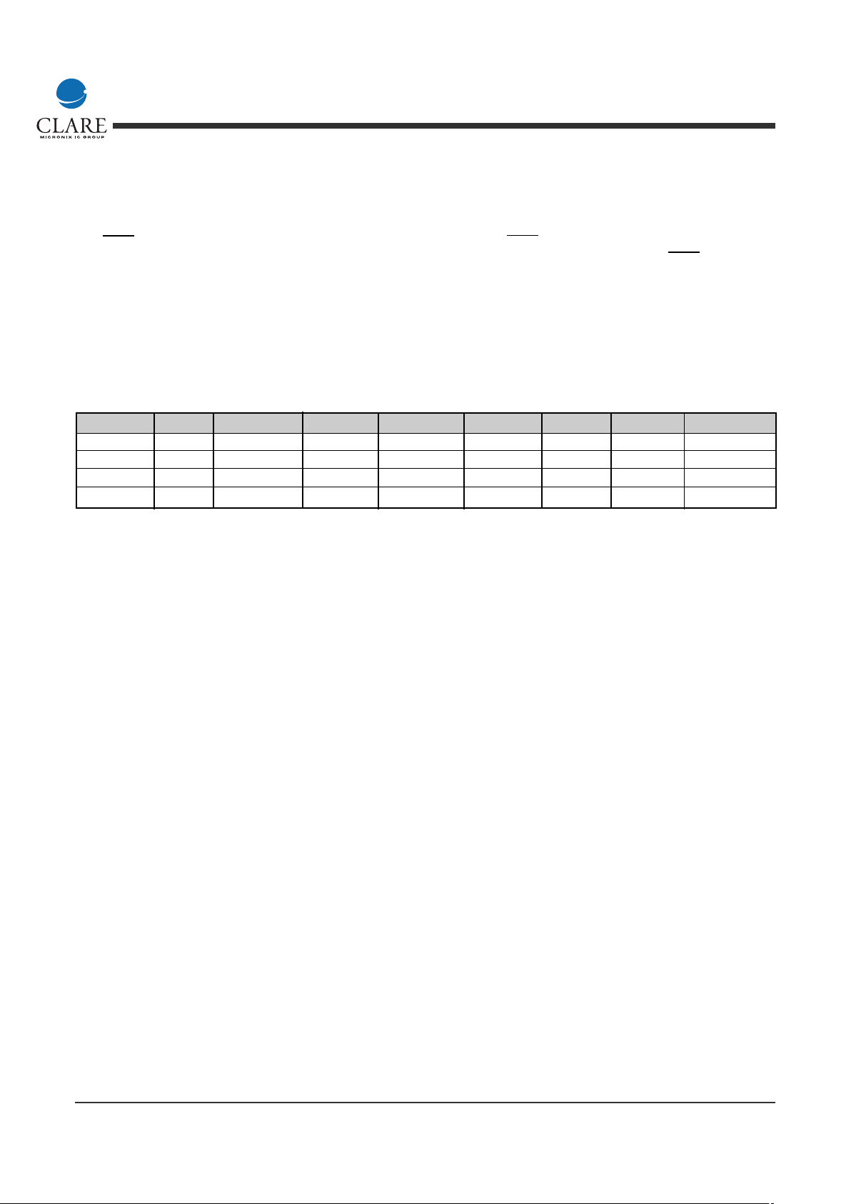
SDM1 SDM0 Mode Line 1 Line 2 Line 3 Line 4 Line 5 Line 6
1 1 Stripe ABC ABC ABC ABC ABC ABC
1 0 Diagonal ABC CAB BCA ABC CAB BCA
0 1 Mosaic Intv BCA BCA BCA BCA BCA BCA
0 0 Mosaic ABC BCA ABC BCA ABC BCA
Note: there is no effect on the DA, DB, DC data buses and which banks they load. Under all SDM1, 0 conditions, DA loads banks 1,4,7,…,190, DB loads banks 2,5,8,…,191, and DC loads banks 3,6,9,…,192.
Functional Description (continued)
Output Current Turn-Off Control
The SWC input signal controls turn-off of the driver outputs. When the SWC signal is high, each output is switched
to ground when the data count is matched and simultaneously disables the current source. When SWC is low, each
output remains in a tri-state condition from when the current source is disabled until the counter equals 63.
SDM Function
The SDM1 and SDM0 inputs determine how the A, B, and C display output banks are configured. They may also be
used to generate special effects in the display. When the SDM signals are open or high, the MXED101 is in its normal operating mode (stripe mode). The SDM mapping to screen configuration is updated each time LE goes high
and is as follows:
Page 8
www.clare.com
8
MXED101
Rev. 9
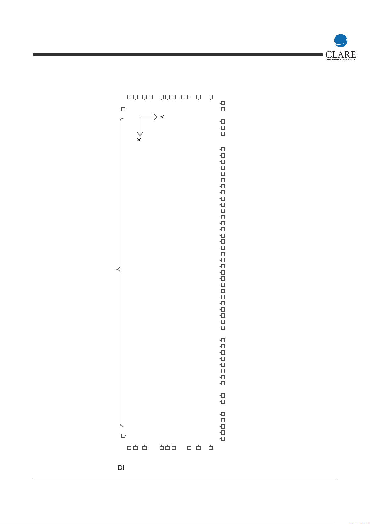
X
Y
Die size is 18,7856 x 2,684 microns
TST(1)
PIN 10
RTKNB
PIN 9
LTKNB
PIN 60
TST(2)
TST(3)
TST(4)
TST(5)
TST(6)
TST(7)
GND
DIRTKN
GA(1)
GB(1)
GC(1)
SMD(1)
SMD(0)
RSTB
VCC
SWC
TGR
GA(2)
GA(0)
GB(2)
GC(2)
GB(0)
GC(0)
DC(5)
DC(4)
DC(3)
DC(2)
DC(1)
DC(0)
DB(5)
DB(4)
DB(3)
DB(2)
DB(1)
DB(0)
DA(5)
DA(4)
DA(3)
DA(2)
DA(1)
DA(0)
STBY
TST(8)
TST(9)
LE
CLKEX
CLKSH
GND
PIN 59
VCC
GND
TST(0)
VDD
VDD
VDD
TEST(2)
ISHRT
ISHRT
PIN 1
GND
GG
RG
VDD
VDD
VDD
TEST(0)
TEST(1)
ISHRT
ISHRT
PIN 70
IOUT1
PIN 71
Q192
PIN 262
REST OF 192 CHANNEL OUTPUT PADS
MXED101 DIE PINOUT
NOT TO SCALE
(0,0) AT CENTER OF PIN 70
Die Size and Pad Locations:
Page 9
MXED101
www.clare.com
9
Rev. 9
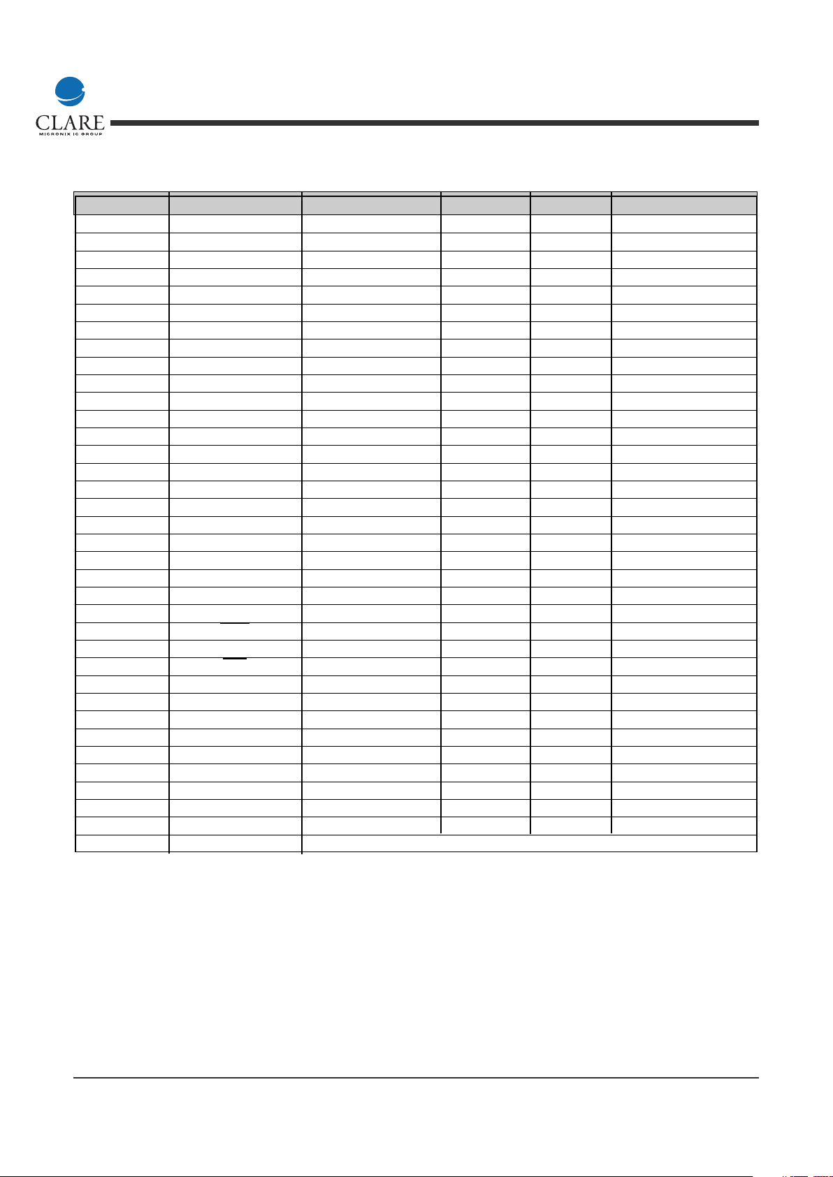
MXED101 Product Description
Pad Name Pad Location (in microns) Pad Name Pad Location (in microns)
1 ISHRT 18392,338 36 DC(3) 11272,2352
2 ISHRT 18392,511 37 DC(2) 11042,2352
3 TEST(2) 18392,693 38 DC(1) 10814,2352
4VDD18392,854 39 DC(0) 10584,2352
5VDD18392,1027 40 DB(5) 7781,2352
6VDD18392,1201 41 DB(4) 7552,2352
7 TST(0) 18392,1383 42 DB(3) 7322,2352
8 GND 18392,1543 43 DB(2) 7093,2352
9 RTKNB 18392,1805 44 DB(1) 6864,2352
10 TST(1) 17997,2352 45 DB(0) 6635,2352
11 TST(2) 17823,2352 46 DA(5) 6406,2352
12 TST(3) 17650,2352 47 DA(4) 6232,2352
13 TST(4) 17476,2352 48 DA(3) 6058,2352
14 TST(5) 17302,2352 49 DA(2) 5885,2352
15 TST(6) 15086,2352 50 DA(1) 5711,2352
16 TST(7) 14910,2352 51 DA(0) 5538,2352
17 GND 14736,2352 52 STBY 1920,2352
18 DIRTKN 14542,2352 53 TST(8) 1747,2352
19 GA(1) 14368,2352 54 TST(9) 1573,2352
20 GB(1) 14195,2352 55 LE 1400,2352
21 GC(1) 14021,2352 56 CLKEX 1226,2352
22 SDM(1) 13848,2352 57 CLKSH 1052,2352
23 SDM(0) 13674,2352 58 GND 209,2352
24 RSTB 13500,2352 59 V
CC
35,2352
25 V
CC
13327,2352 60 LTKNB 0,1739
26 SWC 13153,2352 61 GND 0,1543
27 TGR 12980,2352 62 GG 0,1383
28 GA(2) 12806,2352 63 RG 0,1214
29 GA(0) 12632,2352 64 V
DD
0,1032
30 GB(2) 12459,2352 65 V
DD
0,858
31 GB(0) 12285,2352 66 V
DD
0,685
32 GC(2) 12112,2352 67 TEST(0) 0,524
33 GC(0) 11938,2352 68 TEST(1) 0,356
34 DC(5) 11730,2352 69 ISHRT 0,182
35 DC(4) 11501,2352 70 ISHRT 0,0
71-262 Q(1-192) 427 + 92*(N-1), 129 where N =1 to 192
Note: Pad location reference is to bottom left-hand corner.
Page 10
www.clare.com
10
MXED101
Rev. 9
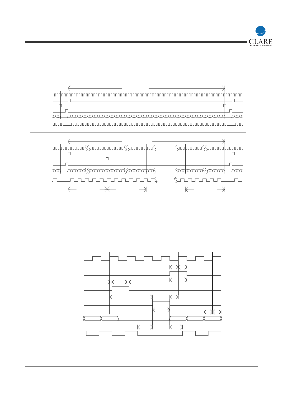
64 DATA CYCLES
64
1
64
1
N * 64 DATA CYCLES
N*64 1N*64 12864
LOAD 1ST DIE LOAD 2ND DIE LOAD NTH DIE
1
MICRONIX INTEGRATED SYSTEMS INC
Aliso Viejo, California 62656
SCALE
SHEET
11133
A
-
0F4G3 B
SIZE DWG NO. REVFSCM NO.
PROJ/PROD NO.
MXHV101
TIMING1
FIGURE 2
LOAD DATA PATTERN MACRO TIMING
CLKSH
LTKNB (IN)
LE
RTKNB (OUT)
1 DIE DISPLAY - LOAD ONE 64 BIT PATTERN FROM LEFT
CLKEX
641
DA/DB/DC(5-0)
CLKSH
LE
N DIE DISPLAY - LOAD N 64 BIT PATTERNS FROM LEFT
LTKNB - 1ST DIE
RTKNB - 1ST DIE
1 64
CLKEX
DA/DB/DC(5-0)
Timing Diagrams - Load Data Pattern Timing
tTPW
tTHDtTSU
tSTD tSTD
tDLD tLDD
N*64 1
tDSU tDHD
tLAPW
tLEDtDLE
LOADING DATA FROM LEFT
LOAD DATA PATTERN TIMING
LTKNB (IN)
CLKSH
RTKNB (OUT)
LE
CLKEX
DA/DB/DC(5-0)
1
6
4
Page 11
MXED101
www.clare.com
11
Rev. 9
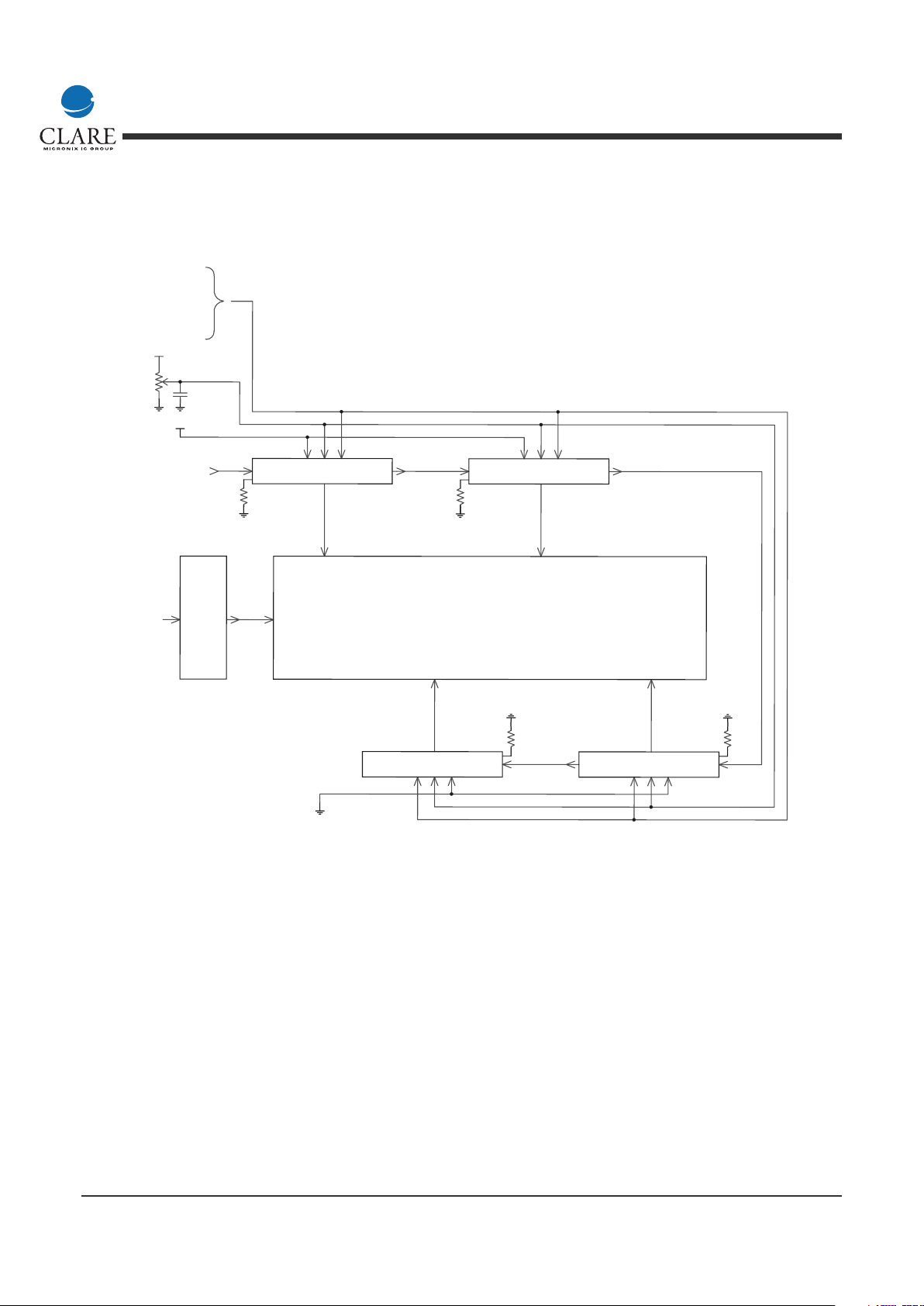
Application note:
NOTE: DATA ORDER FOR DA/DB/DC (5-0) WOULD BE 1-192, 386-576, 577-768, 193-384
CLKSH
LE
DA/DB/DC(5-0)
CLKEX
TGR
GA/GB/GC(2-0)
SWC
12V
GG
VCC
DIRTKN
TOKEN BIT
LTKNB
MXED101
MXED101
RTKNB LTKNB
RTKNB
NROWS
ROW
DATA
ORGANIC LIGHT EMITING DIODE ARRAY
768 X N ELEMENTS
MXED101
MXED101
RTKNB LTKNB
RTKNB
DIRTKN
CHAN 193 - 384
CHAN 1 - 192
10.8K
10.8K
10.8K
10.8K
CHAN 385 - 576
CHAN 577 - 768
ARRAY OF N
SWITCHES TO GND
Page 12

www.clare.com
12
MXED101
Rev. 9
Notes:
Page 13

MXED101
www.clare.com
13
Rev. 9
Notes:
Page 14

CLARE LOCATIONS
Clare Headquarters
78 Cherry Hill Drive
Beverly, MA 01915
Tel: 1-978-524-6700
Fax: 1-978-524-4900
Toll Free: 1-800-27-CLARE
Clare Micronix Division
145 Columbia
Aliso Viejo, CA 92656-1490
Tel: 1-949-831-4622
Fax: 1-949-831-4628
SALES OFFICES
AMERICAS
Americas Headquarters
Clare
78 Cherry Hill Drive
Beverly, MA 01915
Tel: 1-978-524-6700
Fax: 1-978-524-4900
Toll Free: 1-800-27-CLARE
Eastern Region
Clare
P.O. Box 856
Mahwah, NJ 07430
Tel: 1-201-236-0101
Fax: 1-201-236-8685
Toll Free: 1-800-27-CLARE
Central Region
Clare Canada Ltd.
3425 Harvester Road, Suite 202
Burlington, Ontario L7N 3N1
Tel: 1-905-333-9066
Fax: 1-905-333-1824
Western Region
Clare
1852 West 11th Street, #348
Tracy, CA 95376
Tel: 1-209-832-4367
Fax: 1-209-832-4732
Toll Free: 1-800-27-CLARE
Canada
Clare Canada Ltd.
3425 Harvester Road, Suite 202
Burlington, Ontario L7N 3N1
Tel: 1-905-333-9066
Fax: 1-905-333-1824
EUROPE
European Headquarters
CP Clare nv
Bampslaan 17
B-3500 Hasselt (Belgium)
Tel: 32-11-300868
Fax: 32-11-300890
France
Clare France Sales
Lead Rep
99 route de Versailles
91160 Champlan
France
Tel: 33 1 69 79 93 50
Fax: 33 1 69 79 93 59
Germany
Clare Germany Sales
ActiveComp Electronic GmbH
Mitterstrasse 12
85077 Manching
Germany
Tel: 49 8459 3214 10
Fax: 49 8459 3214 29
Italy
C.L.A.R.E.s.a.s.
Via C. Colombo 10/A
I-20066 Melzo (Milano)
Tel: 39-02-95737160
Fax: 39-02-95738829
Sweden
Clare Sales
Comptronic AB
Box 167
S-16329 Spånga
Tel: 46-862-10370
Fax: 46-862-10371
United Kingdom
Clare UK Sales
Marco Polo House
Cook Way
Bindon Road
Taunton
UK-Somerset TA2 6BG
Tel: 44-1-823 352541
Fax: 44-1-823 352797
ASIA PACIFIC
Asian Headquarters
Clare
Room N1016, Chia-Hsin, Bldg II,
10F, No. 96, Sec. 2
Chung Shan North Road
Taipei, Taiwan R.O.C.
Tel: 886-2-2523-6368
Fax: 886-2-2523-6369
http://www.clare.com
Worldwide Sales Offices
Specification: DS-MXED101-R9
©Copyright 2000, Clare, Inc.
All rights reserved. Printed in USA.
3/7/01
Clare cannot assume responsibility for use of any circuitry other
than circuitry entirely embodied in this Clare product. No circuit
patent licenses nor indemnity are expressed or implied. Clare
reserves the right to change the specification and circuitry, without notice at any time. The products described in this document
are not intended for use in medical implantation or other direct life
support applications where malfunction may result in direct physical harm, injury or death to a person.
 Loading...