

Page 1
1
www.clare.com
MXED202
DS-MXED202-R2
The MXED202 Row Driver supports up to 128-row
OLED panel displays. The MXED202 has low "on"
switch resistance, and support of voltage precharge
options, ensures uniform luminance at rapid row scan
rates. This is the first ASSP production row driver for
OLED display OEM's, enabling the development and
manufacture of this new standard in flat-panel display
technology.
• CMOS High Voltage Process: 9V-30V Display Panel
Supply Compatible
• 128 Output Channels, Cascadable; Configurable
120-Output Mode
• 150mA Maximum Current Capability per channel
(two channels maximum active simultaneously)
• 20 Ohm Maximum Row Switch “On” Resistance
• Token-Based Control: Bidirectional data transfer;
Single and Dual-Token Mode
• Current Source Magnitude User Control:
4 µA to 1 mA
• 6-Bit Monochromatic/Color Gray-Scale User Control
• Monochromatic Voltage Precharge Options
• 3.3 V to 5 V logic supply
• Up to 100kHz clock frequency
• Gold-Bumped Die @ ~ 60 micron Output Pitch
• TCP packaging
• Companion to MXED102
240-Channel OLED Column Driver
Features
Description
128-Channel OLED Row Driver
For All Passive-Matrix Organic-Light-EmittingDiode Displays
• Monochrome and Color
• Small-Molecule and Polymer
• Common-Cathode Row Switching
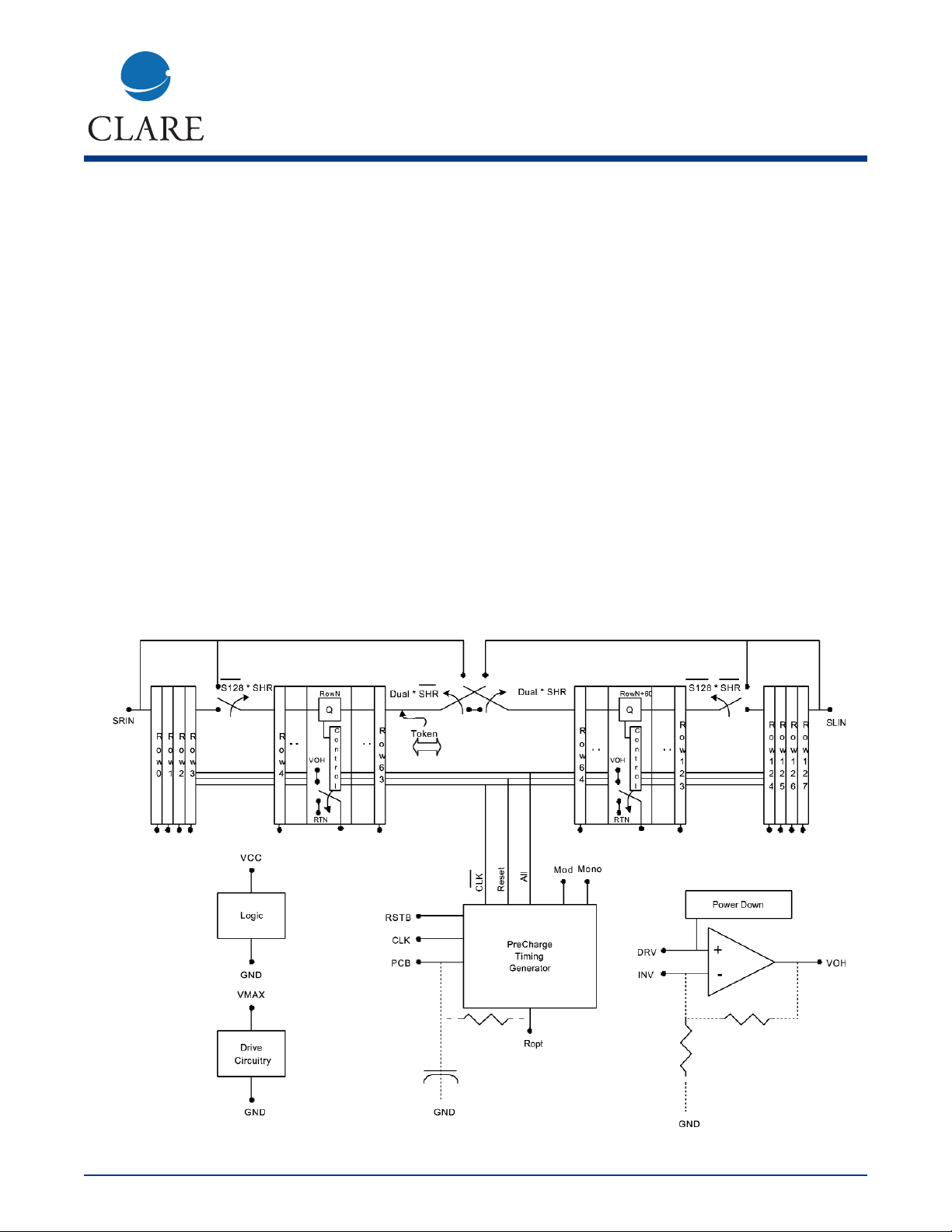
Functional Block Diagram
Preliminary
Page 2

www.clare.com
2
MXED202
Rev. 2
Overview
A row-scan token bit is passed along the length of MXED202 shift register to successively activate the row switches. The OLED cathodes of the active row(s) are switched to RTN, a low impedance return, ground or 0V typically,
while the companion column drivers source data-driven currents through each OLED to be illuminated. Inactive rows
are connected to a programmable "Off" (or Precharge) voltage to ensure the OLED's are not forward-biased. A programmable precharge interval and programmable precharge voltage are available to set initial conditions for the next
active row(s).
In normal, or single token mode, the token may be entered at either end of the MXED202 row shift register (SRIN
or SLIN), depending on the shift direction selection Shift Right (SHR). The token is shifted one row (one channel)
per clock cycle, CLK. One row maximum is active at a time. In dual mode (DUAL), the token is entered at one end
and
automatically in the center, and again the tokens may be selectively shifted left or right at the CLK rate; two rows
maximum are active at a time. The MXED202 has options for 128- and 120-row display panels. When the Select
128 (S128) pin is tied low, the token is also automatically entered at the fifth cell from the entry direction end; only
the 120 middle outputs, Rows 4 through 123, should be used. Note that a lesser number of rows may be used by
resetting the MXED202 (RSTB) at any time, truncating the shift cycle.
Overview of Operation
A row-scan token bit is passed along the length of MXED202 shift register to successively activate the row switches. The OLED cathodes of the active row(s) are switched to RTN, a low impedance return, ground or 0V typically,
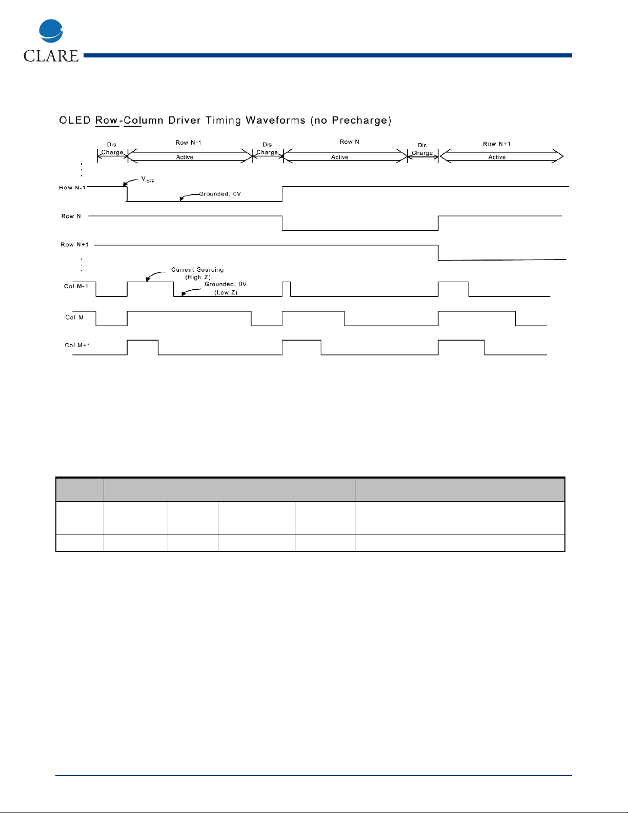
while the companion column drivers source data-driven currents through each OLED to be illuminated. Three successive row activations, N-1, N, N+1, are depicted in the simplified timing diagram below. Inactive rows are connected to a programmable "Off" (or Precharge) voltage to ensure the OLED's are not forward-biased. A
programmable precharge interval and programmable precharge voltage are available to set initial conditions for the
next active row(s). Precharge is described on page 9.
PRELIMINARY ELECTRICAL DATA SHEET
The MXED202 is a row-multiplexed display driver, for Passive Matrix Organic Light Emitting Diode (OLED) and
Polymer Light Emitting Diode arrays (PLED, PolyLED, LEP, . . .), with anodes connected to current-sourcing column
data drivers. The common cathode rows (channels) of the display matrix are activated by sequentially switching
them to a low impedance voltage source (ground/0V, typically) in synchronism with the digital data column current
drive. The MXED202 supports precharging options to improve luminance control. It is manufactured in a high voltage (30 V) CMOS process and provided in bumped die and TCP (Tape Carrier Package) form.
Preliminary
Page 3
MXED202
www.clare.com
3
Rev. 2
Simplified Timing Diagram
Token:
The row-scan token(s) activate row switches. Token entry positions, 0 to 127, are defined in the table below:
Preliminary
S128 DUAL • SHR Outputs Used
00 01 10 11
0 127,123 0,4 127,123,63 0,4,64 Rows 4-123
(Rows 0-3, 124-127 N/C)
1 127 0 127,63 0,64 Rows 0-127
Page 4
www.clare.com
4
MXED202
Rev. 2
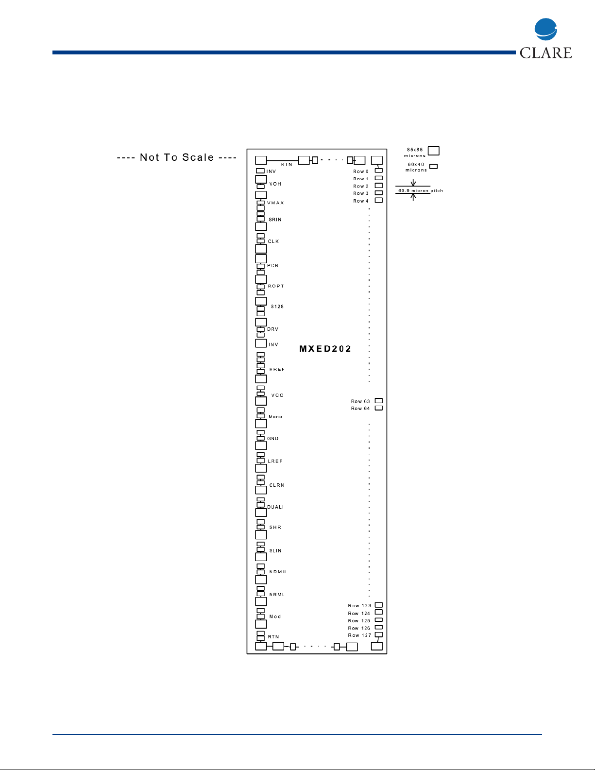
PACKAGE AND PINOUT
This drawing illustrates the pin ordering and relative locations of the bond pads, only. See the MXED202
Semiconductor Die specification
(2)
for exact coordinates.
Top View:
Preliminary
Page 5
MXED202
www.clare.com
5
Rev. 2
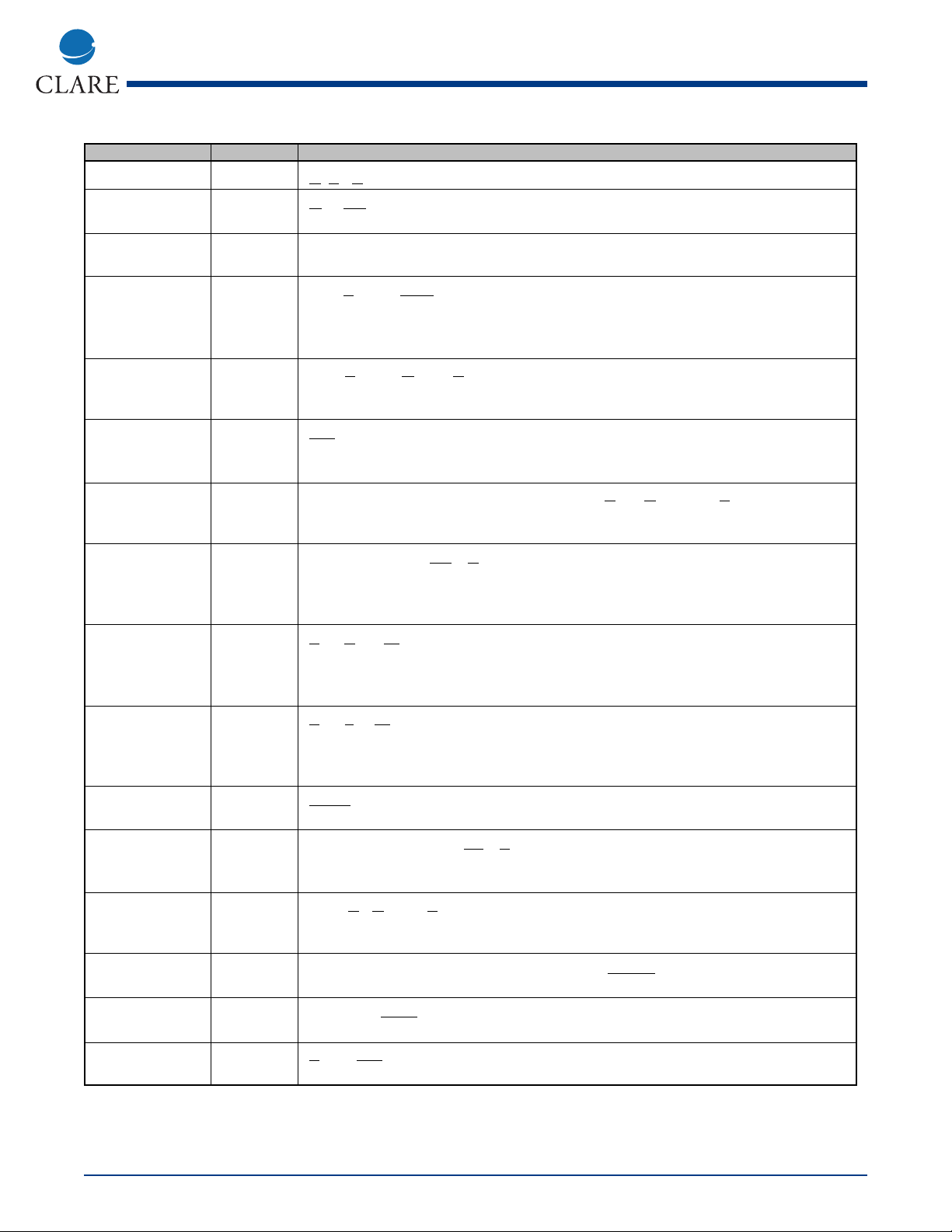
Name I/O/A Description
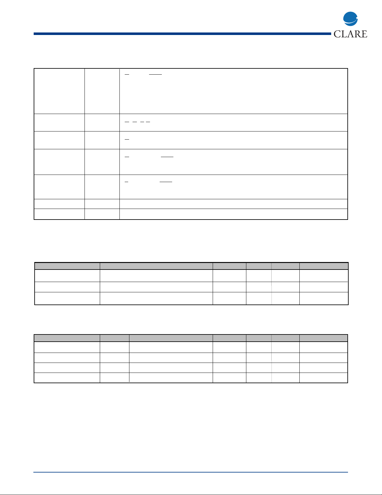
RTN I ReTurN for all display current. (Low impedance ground connection, typically)
GND I GrouND, the negative return for all chip current and the digital logic "zero" refer
ence level.
VCC I The logic voltage positive supply. MXED202 logic operates between VCC and
VSS. Digital inputs should not exceed VCC, VSS
VMAX I This V
oltage MAXimum is the highest positive power supply voltage present on
the chip, and supplies the display panel precharge current either directly or at
derived voltage VOH. Inputs to the chip should not exceed VMAX to avoid for
ward biasing substrate diodes.
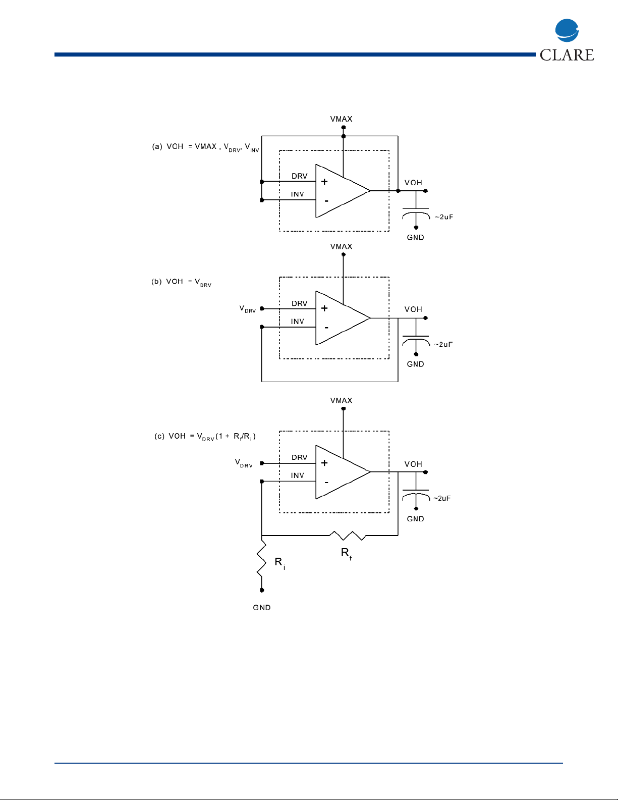
VOH I/O/A Row V
oltage Output High supply. This pin is normally connected to an external
[Page 12] power supply pin VMAX with bypass capacitor, and to pin DRV. Alternatively, an
internal amplifier can generate VOH from an input voltage DRV.
INV I INV
erting input to Voltage Regulator Op Amp, to which an input Resistor RI and
[Page 12] feedback Resistor RF may be connected to develop VOH from VDRV; see DRV
pin.
DRV I When not connected to VOH and VMAX, a D
rive Reference Voltage >1V can be
[Page 12] connected to the DRV pin.Note: If VDRV <0.3V, all row circuitry is powered
down.
SHR I Active high static SHift Right control input: When SHR=1, the token bit travels
from R0 to R127, with SRIN being the token input, SLIN the token output. When
SHR=0, the token bit travels from R127 to R0, with SLIN being the token input,
SRIN the token output. SHR should always be driven to the desired logic level.
SRIN I/O Shift Right INput. This bi-directional pin is the token input when SHR is high, and
the token output (for synchronization or cascading) when SHR is low. When con
figured as an input, this pin should always be driven. Normally low, SRIN should
be driven high once per frame to enter the token into the shift register.
SLIN I/O S
hift L
eft INput. This bi-directional pin is the token input when SHR is low, and
the token output (for synchron- ization or cascading) when SHR is high. When
configured as an input, this pin should always be driven. Normally low, SLIN
should be driven high once per frame to enter the token into the shift register.
DUAL I DUAL
tokens are seeded into the first and middle shift register cells from SRIN
or SLIN when DUAL is static active high. When low, a single token is active.
CLK I The rising edge of the CL
ocK input shifts the token along the internal shift regis
ter to activate successive rows. The display Row Scan Rate is the CLK frequen
cy times the number of tokens.
PCB I If the P
reCharge Bar input is low on the rising edge of CLK, all row outputs will
[Pages 9-11] be switched to the same voltage (see MONO) to enable display panel precharg
ing until PCB returns high. Holding PCB high disables MXED202 precharge.
MONO I Enables MXED202 row driver precharge of MONOchromatic displays, if PCB=0.
[Pages 9-11] The MONO input has no effect if PCB=1.
MOD I This input MODifies precharge timing
[Pages 9-11]
S128 I Select 128 row driver output mode when static active high. When low, 120 row
driver output mode is selected.
PIN LIST
Preliminary
Page 6
www.clare.com
6
MXED202
Rev. 2
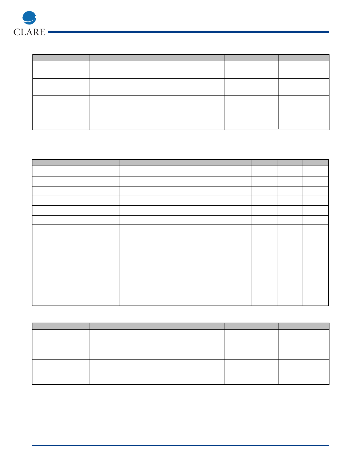
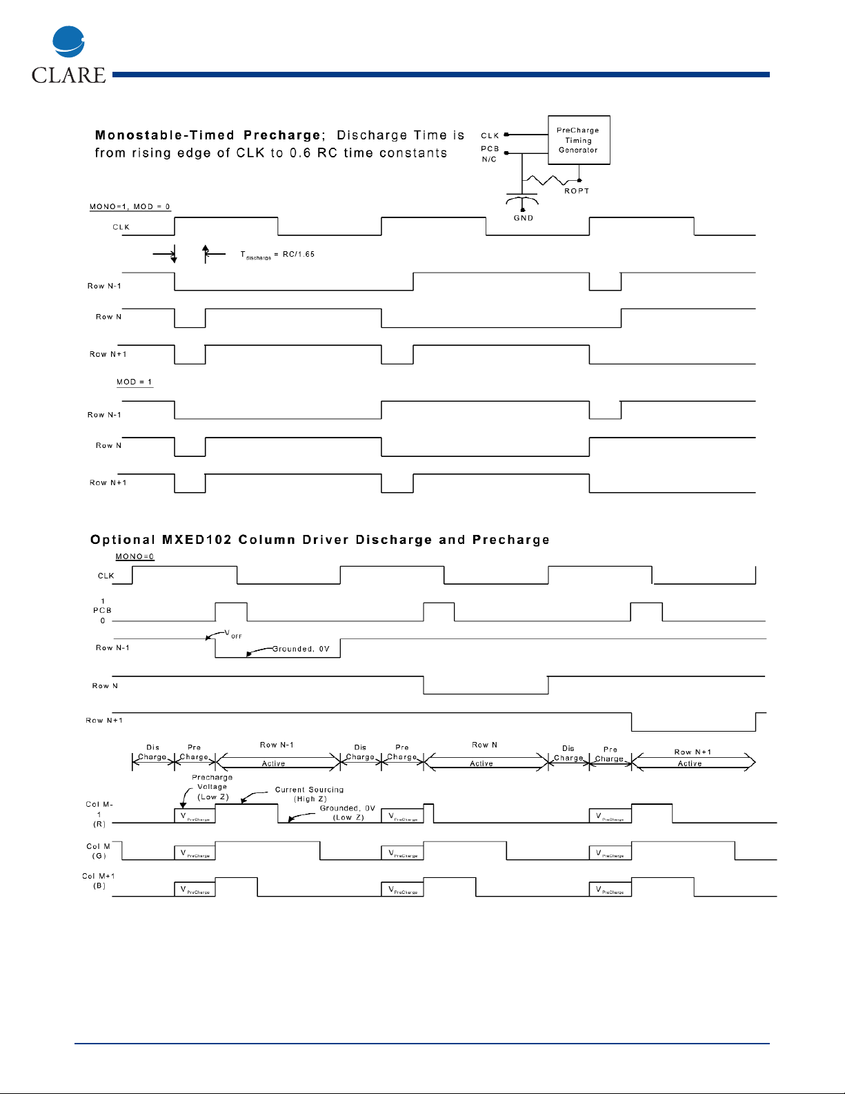
ROPT I/O/A Resistor OPTion pin, normally N/C for digitally controlled precharge timing (PCB),
[Pages 10-11] or when precharge is disabled. When a resistor R is connected between ROPT
and PCB, and a capacitor C is connected between PCB and VSS, the precharge
time will be RC/1.65 when measured from the rising edge of CLK to the falling
edge of ROPT. The timing components should be selected such that RC/1.65 not
exceed 10% of the row active time.
RSTB I R
eSeT Bar, static, active low reset input, clears all the shift register cells, elimi
nating token content.
R(n) O R
ow driver outputs. R(0)-R(127) are used in 128 output mode, S128=1. Only
R(4)-R(123) should be connected when S128=0.
HREF O H
igh voltage REF
erence is an internally generated PFET switch drive voltage
(approximately five-volts less than VOH), which should be bypassed to VOH with
a 2200pF external capacitor.
LREF O L
ow voltage REFerence is an internally generated NFET switch drive voltage
(approximately five-volts above GND), which should be bypassed to GND with a
2200pF external capacitor.
NRMH O Test Pin, N/C
NRML O Test Pin, N/C
ELECTRICAL SPECIFICATION
Note: positive currents flow into the part, negative currents flow out of the part.
Absolute Maximum Ratings:
Operating Conditions:
Unless otherwise stated, all parameters are specified for the following operating conditions.
Pin List (Continued)
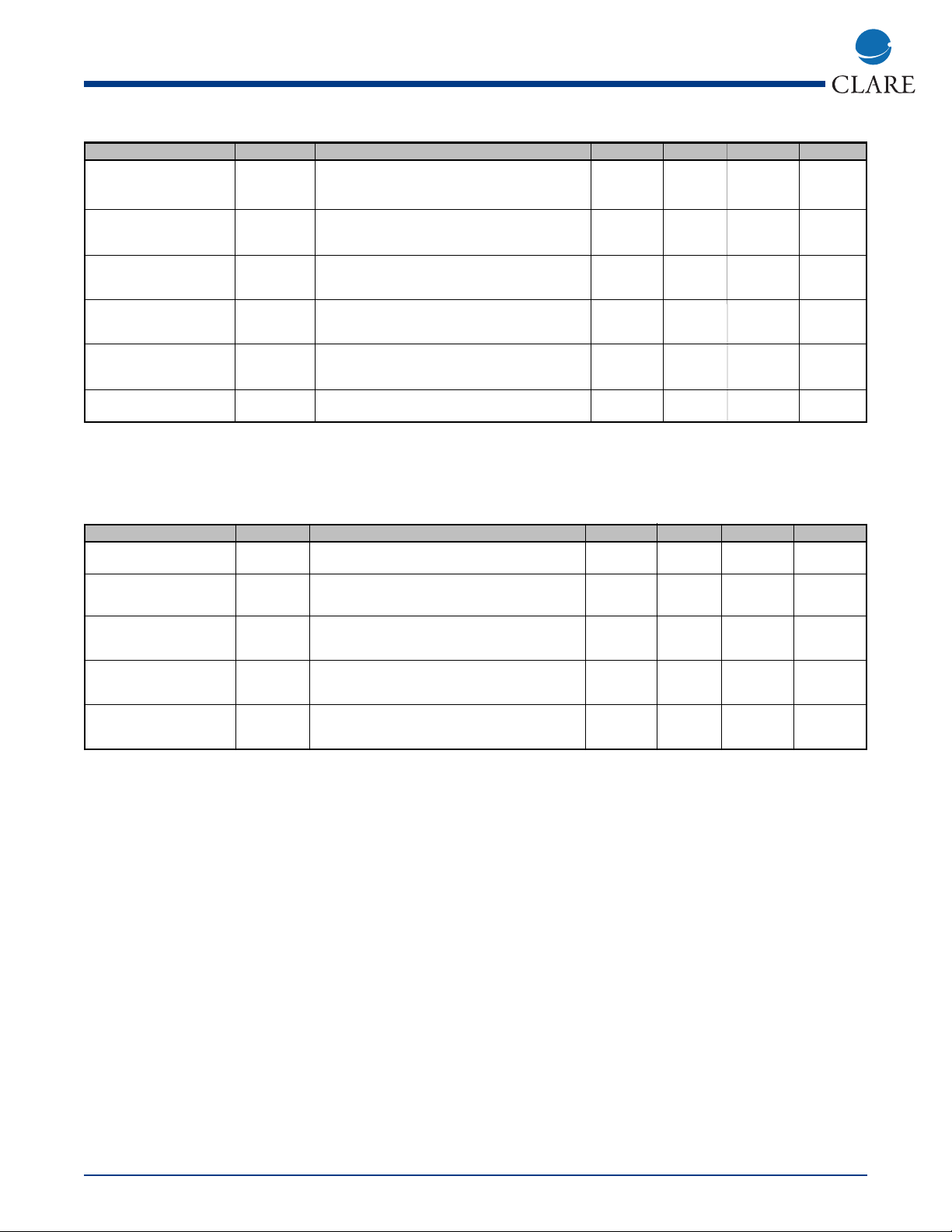
Parameter Operating Condition Min Typ Max Units
Ambient temp - -65 155
o
C
Low voltage supply - -0.3 7.0 V
High voltage supply - -0.3 35.0 V
Parameter Sym Operating Condition Min Typ Max Units
Ambient temp TA - 0 - 70
o
C
Low voltage supply VCC - 3.0 - 5.5 V
High voltage supplies VMAX - 5.0 - 30 V
Clock Frequency CLK - - - 100 kHz
Preliminary
Page 7
MXED202
www.clare.com
7
Rev. 2
Chip Supply Currents - Exclusive of Load
Digital Inputs: SHR, SRIN, SLIN, DUAL, CLK, PCB, MONO, S128, RSTB
Digital Outputs: SRIN, SLIN, ROPT
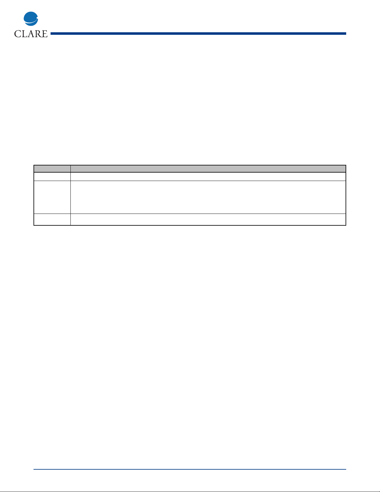
Parameter Sym Operating Condition Min Typ Max Units
Logic Supply, IVCC V
DRV
>1V, f
CLK
<100kHz - 140 210 µA
Operating 3V<VCC<5.5V
Logic Supply, IVCC V
DRV
<0.3V, 3V<VCC<5.5V - 15 25 µA
Powerdown
High Voltage IVMAX V
DRV
>1V, f
CLK
<100kHz
Supply, Operating 9V<MAX<30V - 445 700 µA
High Voltage Supply, IVMAX V
DRV
<0.3V, 9V<MAX<30V - - 20 µA
Powerdown
Parameter Sym Operating Condition Min Typ Max Units
Input low voltage VIL - - - 0.4 V
Input high voltage VIH - VCC-0.4 - - V
Input current II - -10 - 10 µA
Clock Rise Time CLK
RT
---5nS
Clock Fall Time CLK
FT
--5nS
Clock Duty Cycle CLK
%
-20-80%
Setup Time T
Set
Time in advance of 10% rising edge 50 - - nS
of CLK that inputs SHR, SRIN, SLIN,
DUAL, PCB, MONO, S128, CLRB
must be at valid input logic levels
to take effect on next clock cycle.
Hold Time T
Hold
Time subsequent to 90% rising edge 50 - - nS
of CLK that inputs SHR, SRIN, SLIN,
DUAL, PCB, MONO, S128, CLRB
must be valid to take effect on next
rising edge of the clock (CLK).
Parameter Sym Operating Condition Min Typ Max Units
Output low voltage VOL Iout = 200 µA - - 0.4 V
Output high voltage VOH Iout = -200 µA VCC-0.4 - - V
Output rise/fall time TRF 10 to 90 %, Cload = 5 pF - - 5 nS
Precharge Timing R
ROPT
Pages 9-11 50 - 200 kΩ
Resistor connected
to pin ROPT
Preliminary
Page 8
www.clare.com
8
MXED202
Rev. 2
Analog Inputs: DRV, INV
Analog Outputs: VOH, HREF, LREF, R(n)
Bypass capacitors to GND: CVOH=10µF; CHREF, CLREF =2nF
Parameter Sym Operating Condition Min Typ Max Units
DRV Pin Input DRV
Rin
-10--kΩ
Resistance
DRV Pin Input DRV
Cin
---10pF
Capacitance
Voltage Range of V
DRV
- 1.0 -
VMAX-1.5 V
DRV Input
Feedback Resistor R
F
- 10 - 100 kΩ
from VOH to INV
Input Resistor from R
I
- 10 - 100 kΩ
INV to GND
Gain Ratio R
F
/ R
I
- 0.1 - 10 -
Parameter Sym Operating Condition Min Typ Max Units
Precharge Voltage VOH Iout
avg
= 100 µA, CLOAD=1000pF 5 - 30 V
Precharge Ripple VOH
ac
Voltage Regulator Active, - - 100 mV
Iout
avg
= 100 µA p-p
Row 0-127 Output Row
ON
VROW < 5V
Pulldown Resistance (to enable OLED turn-on) - - 20 Ω
Row 0-127 Output Row
OFF
VROW > (VOH-2V)
Pullup Resistance (to disable OLED turn-on) - - 300 Ω
Row 0-127 Chip C
Row
Per output - - 20 pF
Output Capacitance
Preliminary
Page 9
MXED202
www.clare.com
9
Rev. 2
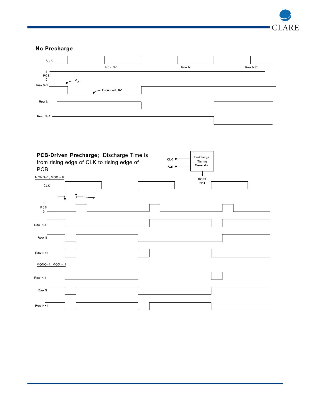
PRECHARGE:
(Organic) Light-Emitting Diodes are current controlled devices, their photonic output (luminance) being proportional
to the time-average charge passed through them. To pass charge, the forward voltage must first reach the diode
“on” threshold. In passive-matrix panel displays, OLED’s are connected in n-row x m-column matrix fashion. In the
row multiplex scheme, where a single row of OLED’s is activated at a time, the parasitic capacitance of the n-1 “off”
rows of OLED’s appears connected to the columns - this capacitance must be charged to the “on” threshold before
current flows through the selected “on” row diodes. If the column drive current alone were to charge this capacitance, much of the allotted row time would be consumed in just reaching the “on” threshold. Therefore, to improve
the efficiency of the display, and to make luminance directly proportional to column current-magnitude and currentduty cycle, the MXED102 and MXED202 Display drivers support optional voltage precharge. In all precharge
options, a predetermined voltage is impressed upon the diodes. For instance, the user may configure the precharge
voltage to be near the OLED “on threshold,” to bias the diodes to the onset of conduction.
The Timing Diagrams, Pages 10-11, illustrate the Prechage Options:
Condition Precharge
PCB=1 No Precharge
MONO=1 A Monochromatic Precharge voltage may be applied via the MXED202 Row Driver, as a function of
CLK, PCB, MOD. During the Discharge interval, all Row and Column driver outputs are grounded,
discharging all pixels. At the beginning of the Active interval, a selected Precharge Voltage is applied
to all but the next active row, and the column drivers source data-driven currents.
MONO=0 Color/Monochrome Precharge by the MXED102 Column Driver, as function of CLK, PCB.
Preliminary
Page 10
www.clare.com
10
MXED202
Rev. 2
TIMING DIAGRAMS
Preliminary
Page 11
MXED202
www.clare.com
11
Rev. 2
Preliminary
Page 12
www.clare.com
12
MXED202
Rev. 2
VOH OPTIONS
Preliminary
Page 13

MXED202
www.clare.com
13
Rev. 2
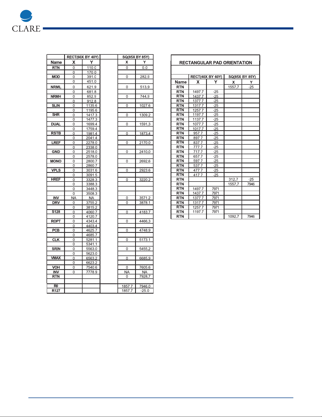
SEMICONDUCTOR DIE DATA SHEET
The MXED202 is a common cathode (row) driver for Passive Matrix Organic Light Emitting Diode (OLED) and
Polymer Light Emitting Diode (PLED, PolyLED, LEP,…etc.) displays, with anodes connected to the columns. This
document specificies the physical and mechanical properties of MXED202 semiconductor die, as provided in wafer
form.
DIMENSIONS
Die Size
“X Dimensions” Center Scribe to Center Scribe: 8270 µm
“Y Dimensions” Scribe to Center Scribe: 2300 µm
Die Thickness
Unthinned (Non Back Lapped Wafer) Thickness: 25 mil
Preliminary
Page 14
www.clare.com
14
MXED202
Rev. 2
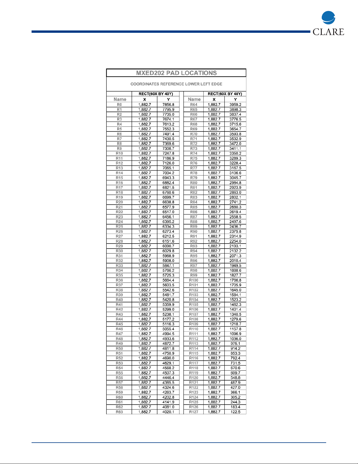
BONDING PADS
Locations and Sizes -Driver Outputs
Preliminary
The information contained on this page is preliminary. Although the order of the bond pad will remain the same, the XY dimensions in the final
document may vary slightly. Please take this possibility into consideration when doing any chip on board layouts.
Page 15
MXED202
www.clare.com
15
Rev. 2
Interface Input/Output
Preliminary
Page 16

www.clare.com
16
Rev. 2
CLARE LOCATIONS
Clare Headquarters
78 Cherry Hill Drive
Beverly, MA 01915
Tel: 1-978-524-6700
Fax: 1-978-524-4900
Toll Free: 1-800-27-CLARE
Clare Micronix Division
145 Columbia
Aliso Viejo, CA 92656-1490
Tel: 1-949-831-4622
Fax: 1-949-831-4628
SALES OFFICES
AMERICAS
Americas Headquarters
Clare
78 Cherry Hill Drive
Beverly, MA 01915
Tel: 1-978-524-6700
Fax: 1-978-524-4900
Toll Free: 1-800-27-CLARE
Eastern Region
Clare
603 Apache Court
Mahwah, NJ 07430
Tel: 1-201-236-0101
Fax: 1-201-236-8685
Toll Free: 1-800-27-CLARE
Central Region
Clare Canada Ltd.
3425 Harvester Road, Suite 202
Burlington, Ontario L7N 3N1
Tel: 1-905-333-9066
Fax: 1-905-333-1824
Western Region
Clare
1852 West 11th Street, #348
Tracy, CA 95376
Tel: 1-209-832-4367
Fax: 1-209-832-4732
Toll Free: 1-800-27-CLARE
Canada
Clare Canada Ltd.
3425 Harvester Road, Suite 202
Burlington, Ontario L7N 3N1
Tel: 1-905-333-9066
Fax: 1-905-333-1824
EUROPE
European Headquarters
CP Clare nv
Bampslaan 17
B-3500 Hasselt (Belgium)
Tel: 32-11-300868
Fax: 32-11-300890
France
Clare France Sales
Lead Rep
99 route de Versailles
91160 Champlan
France
Tel: 33 1 69 79 93 50
Fax: 33 1 69 79 93 59
Germany
Clare Germany Sales
ActiveComp Electronic GmbH
Mitterstrasse 12
85077 Manching
Germany
Tel: 49 8459 3214 10
Fax: 49 8459 3214 29
Italy
C.L.A.R.E.s.a.s.
Via C. Colombo 10/A
I-20066 Melzo (Milano)
Tel: 39-02-95737160
Fax: 39-02-95738829
Sweden
Clare Sales
Comptronic AB
Box 167
S-16329 Spånga
Tel: 46-862-10370
Fax: 46-862-10371
United Kingdom
Clare UK Sales
Marco Polo House
Cook Way
Bindon Road
Taunton
UK-Somerset TA2 6BG
Tel: 44-1-823 352541
Fax: 44-1-823 352797
ASIA PACIFIC
Asian Headquarters
Clare
Room N1016, Chia-Hsin, Bldg II,
10F, No. 96, Sec. 2
Chung Shan North Road
Taipei, Taiwan R.O.C.
Tel: 886-2-2523-6368
Fax: 886-2-2523-6369
http://www.clare.com
Worldwide Sales Offices
Specification: DS-MXED202-R2
©Copyright 2001, Clare, Inc.
All rights reserved. Printed in USA.
5/21/01
Clare cannot assume responsibility for use of any circuitry other
than circuitry entirely embodied in this Clare product. No circuit
patent licenses nor indemnity are expressed or implied. Clare
reserves the right to change the specification and circuitry, without notice at any time. The products described in this document
are not intended for use in medical implantation or other direct life
support applications where malfunction may result in direct physical harm, injury or death to a person.
 Loading...