

Page 1
1
www.clare.com
MXED102
DS-MXED102-R2
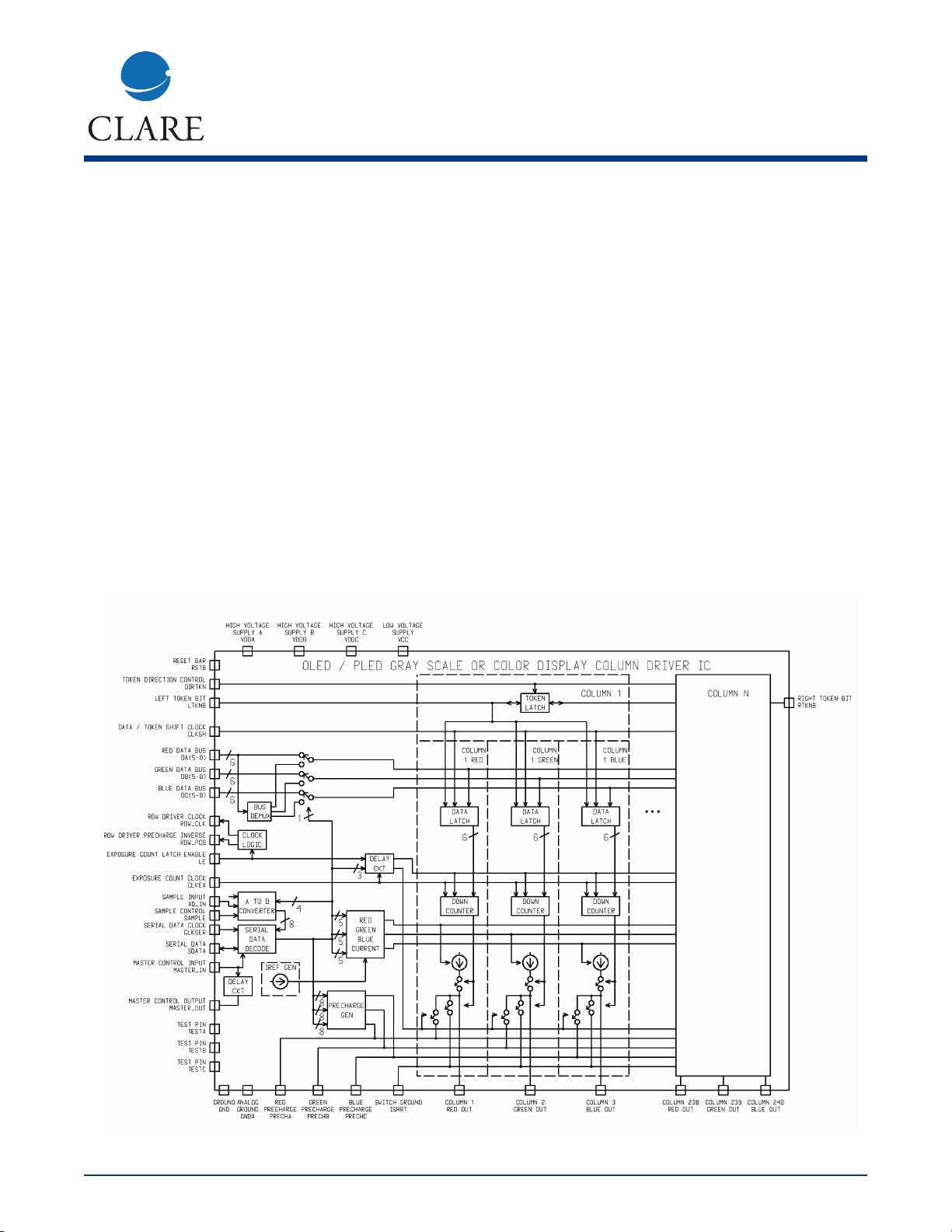
The MXED102 is Clare’s second-generation OLED column driver offering, which supports up to 240-monochromatic or 80-color OLED pixels. The MXED102's
exceptionally tight current-matching of adjacent and
cascaded outputs, precharge options, and OLED monitoring capability, ensures uniform luminance and highquality greyscaling in both monochromatic and RGB
mode. This is the first ASSP production driver for OLED
module OEM's building a new standard in flat-panel displays.
• CMOS High Voltage Process: 9V-30V Display Panel
Supply Compatible
• 240 Output Channels, Cascadable
• Token-Based Bidirectional Data Transfer: Direct User
Control of Scan Rate
• Current Source Magnitude User Control: 4 µA to 1 mA
• 6-Bit Monochromatic/Color Gray-Scale User Control
• Current matching accuracy: ± 2% ± 1.5 µA intra-die
± 1% inter-die
• Monochromatic/Color Voltage Precharge Options
• Built-In A-to-D Converter Monitoring of Display Panel
Characteristics
• 3.3 V to 5 V logic supply
• Up to 35 MHz clock frequency
• Gold-Bumped Die @ 60 micron Output Pitch
• TCP packaging
• Companion to Clare Micronix MXED202
128-Channel OLED Row Driver
Features
Description
240-Channel OLED Column Driver
For All Passive-Matrix Organic-Light-EmittingDiode Displays
• Monochrome and Color
• Small-Molecule and Polymer
• Current-Sourcing Anode Drivers
Column Driver Block Diagram
Preliminary
Page 2
www.clare.com
2
MXED102
Rev. 2
Preliminary
PRELIMINARY ELECTRICAL DATA SHEET
This document is a specification for a digital data driver for Passive Matrix Organic Light Emitting Diode (OLED) and
Polymer Light Emitting displays (PLED, PolyLED, LEP, . . . ,etc) with anodes connected to the columns. The output
stage of each channel has a resistive switch to an on chip generated voltage used during precharge and a current
source used during data output to minimize non-uniformity caused by spatial and temporal variations of the LED
characteristics and by line resistances. The data driver chip is manufactured in a high voltage (30 V) CMOS process
and provided in bumped die and TCP (Tape Carrier Package) form.
Description of Operation:
Overview
: The MXED102 is configured via a serial port, and pixel data is updated on a per-row basis via a parallel
data bus.
Dynamic Pixel Control: Gray-Scale Control data is loaded into the 6-bit Column Exposure Counters each row scan
time, while the previously loaded data is being output to the OLED Display Panel. The control data sets the exposure time from 0 to 63 Exposure Clock times. Successive counters are accessed upon coincidence with the token
bit, which is shifted the length of the MXED102 by the Token Shift Clock. In 6-bit Data Mode, Databus C {DC(5-0)}
is used to enter per-pixel data, and the Token traverses length of the Chip in 240 Token Shift Clocks. In 18-bit Data
Mode, Databusses A, B, and C are used to load three successive pixels in parallel, and the Token traverses length
of the Chip in 80 Token Shift Clocks.
Chip Configuration: A display controller may use the serial bus to set the characteristics of all column driver ICs by
writing to all column driver ICs in parallel. During write, the controller writes the entire data packet. The controller
can also interrogate a single column driver IC, whose MASTER pin is pulled high. Only one column driver IC on a
given bus can be designated as master. During read, the controller writes the preamble, start of frame delimiter, register address, and turn around bits. It then tri-states for the bus tri-state and data bits and reads the data.
Color/Monochrome: The MXED102 supports three-each interleaved column Current Magnitude settings and three
Precharge Voltages, A,B and C, which may be mapped to R,G,B. Monochrome mode is selected by setting the
Color control bit to zero, in which case the Current Magnitude and Precharge Voltage is common.
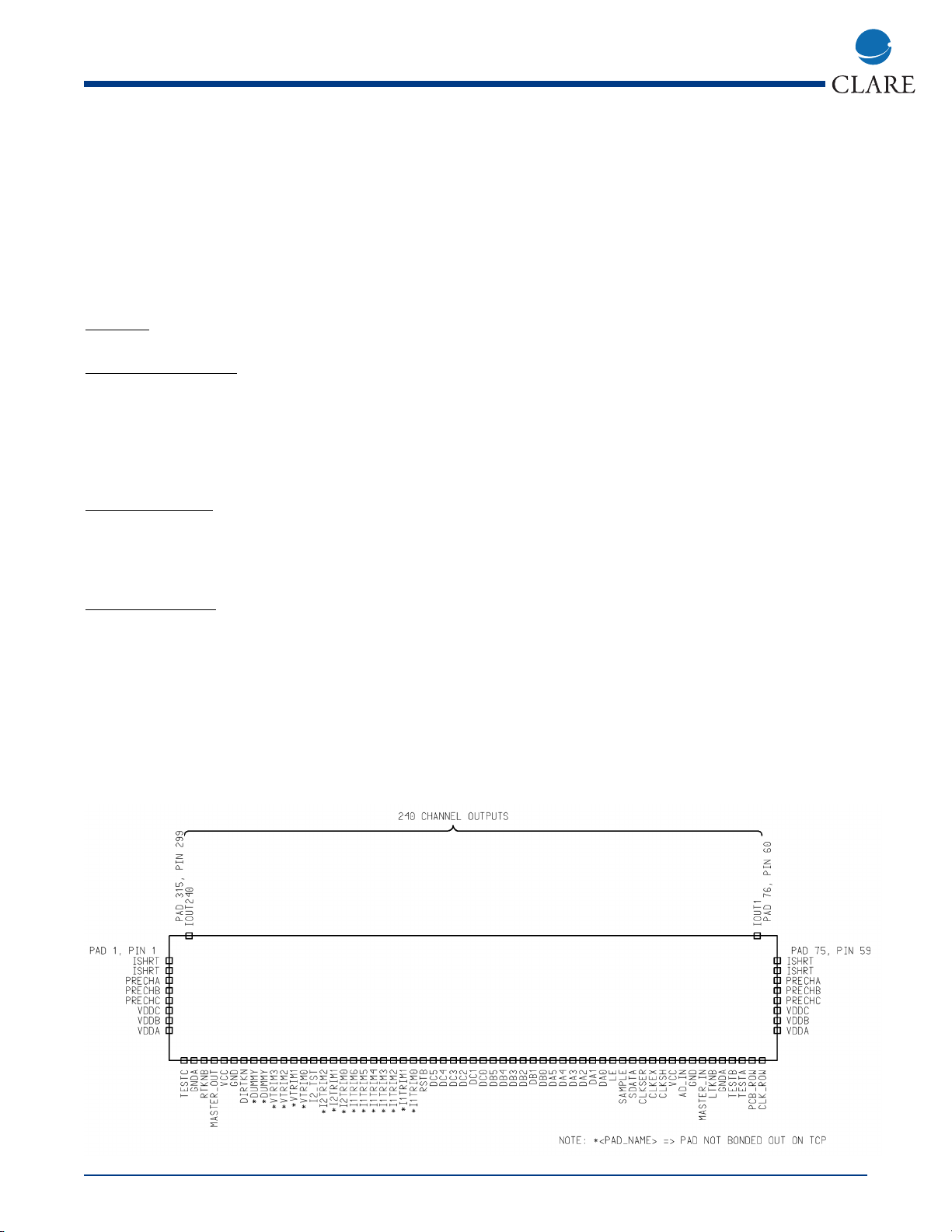
Package and Pin Out
Below is a diagram of the chip pinout:
MXED102 OLED/PLED Column Driver IC Pad Order
(NOT TO SCALE)
(DIE NOT FLIPPED)
Page 3
MXED102
www.clare.com
3
Rev. 2
Pin List
Name I/O/A Description
VDDA, High voltage supply A/B/C:
VDDB, -
VDDC
VCC - Logic supply:
GND - Ground:
GNDA - Analog ground:
ISHRT - Ground used to short output channels: There can be high currents on this line. It
should be separated from the circuit ground pads (GND) to prevent ground bounce.
PRECHA, O/A
PRECHB,
PRECHC
MASTER_IN I Master In: High input implies chip is master. This input is pulled low internally.
MASTER_OUT O Master Out: MASTER_IN delayed by 1 LE clock cycle, sampled on rising edge of LE.
RSTB I Reset Bar: Input signal used to reset digital logic for test purposes. This input is
pulled high internally.
CLKSH I Token Shift Clock: Input signal used to shift tokens down the length of the driver IC
and latch data into the corresponding columns. The direction of token shift is deter
mined by DIRTKN pin.
LTKNB I/O Left Token Bit: Input for shift right, output for shift left. Signal is used to pass the
tokens into and out of the driver IC. High state represents the presence of token.
RTKNB I/O Right Token Bit: Input for shift left, output for shift right. Signal is used to pass the
tokens into and out of the driver IC. High state represents the presence of token.
DIRTKN I Token Direction Input: Input signal which, when high, causes the token to shift left to
right in the driver IC. A low signal causes the token to shift right to left. In the paral
lel data mode the token passes through the chip in 80 CLKSH clocks, in the serial
data mode the token passes through the chip in 240 CLKSH clocks. This input is
pulled high internally.
LE I Latch Enable: Input signal used to begin data output. When data output begins, new
data input for the following row can begin.
DA(5-0), I Data A/B/C: Signal buses used to input the exposure data.
DB(5-0),
DC(5-0)
CLKEX I Exposure Clock: Input signal used to clock the driver IC's exposure counter from 0 to
63 for a row exposure. The signal must be cycled at least 64 times between LE
pulses to completely cycle the counter. Cycles of CLKEX beyond 64 will have no
effect.
CLKSER I Serial Clock: Clock to write serial data into all column drivers or read serial data from
the master column driver.
SDATA I/O Serial Data: Serial data written to all column drivers or read from the master column
driver.
SAMPLE I Initiate A/D sample. This input is pulled low internally.
Precharge A/B/C: Column precharge voltage outputs. PRECHA/B/C should be tied
to PRECHA/B/C of all other column drivers to ensure a uniform display precharge
and should be bypassed to ground with a capacitor at least 50 times the display
capacitance.
Preliminary
Page 4
www.clare.com
4
MXED102
Rev. 2
AD_IN A A to D Input: The part can do an A to D conversion on the voltage on this input.
TESTA, A Test Outputs: The A, B, and C driver bank outputs are muxed to the TESTA, TESTB,
TESTB, and TESTC pads respectively when these pads are pulled low. During normal
TESTC operation they are left open or tied to VDD.
I1TRIM A Current Source 1 Trim: These pins must be left open.
(6:0)
I2TRIM A Current Source 2 Trim: These pins must be left open.
(3:0)
VTRIM A Voltage Source Trim: These pins must be left open.
(3:0)
I2_TST A Current Source 2 Monitor: This pin must be left open.
IOUT(240-1) A Channel Outputs: The outputs of the driver IC that directly drives the display panel
CLK_ROW O Row Clock: Signal intended to drive the row driver IC shift data clock
PCB_ROW O Row Precharge: Signal intended to drive the row driver IC precharge input
Note: A => analog, I => digital input, O => digital output
ELECTRICAL SPECIFICATIONS
Positive currents flow into the part, negative currents flow out of the part, largest currents are currents with the greatest absolute magnitude.
Absolute Maximum Ratings:
Parameter Operating Condition Min Typ Max Units
Ambient temp - -65 - 155
o
C
Low voltage supply - -0.3 - 7.0 V
High voltage supply - -0.3 - 35.0 V
Operating Conditions:
Unless otherwise stated, all parameters are specified for the following operating conditions.
Parameter Sym Operating Min Typ Max Units
Condition
Ambient temp TA - 0 - 70
o
C
Low voltage supply VCC - 3.0 - 5.5 V
High voltage supplies VDDA, - 9.0 - 30 V
VDDB, VDDC
Supply Currents:
Parameter Sym Operating Min Typ Max Units
Condition
High voltage supply IDD - - - TBD uA
current during standby (stby)
Internal high voltage IDD Current from VDD not 14 mA+ mA
supply current during (int) flowing out outputs or - - 12xIout
operation into precharge circuit
Iout = per channel
Low voltage supply ICC - - - TBD uA
current during standby (stby)
Low voltage supply ICC - - - 10 mA
current during operation
Preliminary
Pin List (continued)
Page 5
MXED102
www.clare.com
5
Rev. 2
Digital Inputs:
Parameter Sym Operating Condition Min Typ Max Units
Input low voltage VIL - - - 0.5 V
Input high voltage VIH - VCC-0.5 - - V
Input current II - -10 - 10 uA
Digital Outputs:
Parameter Sym Operating Condition Min Typ Max Units
Output low voltage VOL Iout = 100 uA - - 0.4 V
Output high voltage VOH Iout = -100 uA VCC-0.4 - - V
Output rise/fall time TRF 10 to 90 %, Cload=5 pF - - 2.0 nS
Serial Configuration Bus:
Bus Operation:
The controller uses the serial bus to set the characteristics of all column driver ICs by writing to all column
driver ICs in parallel. During write, the controller writes the entire data packet. The controller can also inter
rogate a single column driver IC, who's MASTER pin is pulled high. Only 1 column driver IC on a given bus
can be designated as master. During read, the controller writes the preamble, start of frame delimiter, reg
ister address, and turn around bits. It then tri-states for the bus tri-state and data bits and reads the data.
Data Packet:
The data packet consists of:
- 14 bit preamble of all 1's
- 2 bit start of frame delimiter (SFD)
- 6 bit register address - MSB first
- 1 turn around bit (TA)
- 1 bus tristate (BT)
- 8 bit data packet - MSB first
Write => write data to all column driver ICs
Read => read data from master column driver IC
Data order => Preamble first, data last; MSB first, LSB last
R/W Preamble SFD Reg Address TA BT Data
write 1111 1111 1111 11 00 AAAA AA 0 0 DDDD DDDD
read 1111 1111 1111 11 01 AAAA AA 0 Z DDDD DDDD
Preliminary
Page 6
www.clare.com
6
MXED102
Rev. 2
Input Registers
Register Address 0 - Test Register
Eight bits of data can be written to and read from this register in order to test the serial port. This register
has no effect on the column driver.
Register Address 1 - Control Register 1
Bit(s) Name Description Default
7 Freeze Master Modes:
1 => MASTER_OUT pin is not changed 0
0 => Normal, MASTER_OUT is updated to
MASTER_IN on rising edge of LE
6 Disable Precharge Driver Modes:
1 => Precharge circuit is disabled 0
0 => Normal
5 Standby Modes:
1 => Part is operating normally 0
0 => Part is in low power standby mode
4 Short Channels Modes:
1 => Channels are all shorted to ground after the 0
CLKEX count reaches 64
0 => Each channel is individually shorted to ground
after its current source is tristated
3 Color Mode Modes:
0 => Monochrome mode 0
1 => Color mode
2 Data Mux Modes:
0 => DA(5-0), DB(5-0), DC(5-0) data words are read 0
serially from the DC(5-0) pins. The DA(5-0) and
DB(5-0) pins are unused.
1 => DA(5-0), DB(5-0), DC(5-0) pins used to read
their respective data words.
1-0 Test Mode(1:0) Modes:
00 => Normal operation 00
01 => Test mode 1
10 => Test mode 2
11 => Test mode 3
Register Address 2 - Control Register 2
Bit(s) Name Description Default
7-2 Undefined - -
1 Fast Conversion Modes: -
- - 0 => Normal operation 0
-- 1 => -
0 High A/D Gain Modes: -
- - 0 => Normal operation 0
Preliminary
Page 7

MXED102
www.clare.com
7
Rev. 2
Register Address 3 - A Output Group Data Current Magnitude Register
The 5 LSB bits determine the magnitude of A output group current during data output.
Register Address 4 - B Output Group Data Current Magnitude Register
The 5 LSB bits determine the magnitude of B output group current during data output.
Register Address 5 - C Output Group Data Current Magnitude Register
The 5 LSB bits determine the magnitude of C output group current during data output.
Register Address 6 - A Output Group Precharge Voltage Magnitude Register
The 8 bits determine the magnitude of A output group voltage during precharge.
Register Address 7 - B Output Group Precharge Voltage Magnitude Register
The 8 bits determine the magnitude of B output group voltage during precharge.
Register Address 8 - C Output Group Precharge Voltage Magnitude Register
The 8 bits determine the magnitude of C output group voltage during precharge.
Register Address 9 - Precharge Count Register
The 3 LSB bits set the precharge time to 0 to 7 CLKEX clock counts.
Register Address 10- A/D Converter Control Register
This register determines which signal is monitored by the A/D converter.
Bit(s) Name Description Default
7-4 UNDEFINED - -
3-0 ad_sel(3:0) 0xF => Measure VDDA ( Low Gain ) 0000
0xE => Measure TESTA ( Low Gain )
0xD => Measure IOUT231 ( Low Gain )
0xC => Measure IOUT6 ( Low Gain )
0xB=> Measure VDDB ( Low Gain )
0xA => Measure TESTB ( Low Gain )
0x9 => Measure IOUT232 ( Low Gain )
0x8 => Measure IOUT7 ( Low Gain )
0x7 => Measure VDDC ( Low Gain )
0x6 => Measure TESTC ( Low Gain )
0x5 => Measure IOUT233 ( Low Gain )
0x4 => Measure IOUT8 ( Low Gain )
0x3 - 0x2 => Undefined
0x1 => Measure AD_IN input ( High Gain )
0x0 => Input grounded
Preliminary
Page 8

www.clare.com
8
MXED102
Rev. 2
Registers 11 thru 63 - Undefined
Output Registers
Register Address 0 - Test Register
Register Address 1 - Status Register 0
Bit(s) Name Description Default
7-0 Undefined - -
Register Address 2 - A/D Converter Output Register
Registers 3 thru 63 - Undefined
Power on Reset:
The part contains a power on reset circuit that ensures that the serial bus data registers come up in their default
value when VCC is cycled on. This brings up the part in its standby mode.
Digital Timing:
Parameter Sym Operating Conditions Min Typ Max Unit
Shift clock frequency - - - - 25 MHz
Shift clock minimum high - - 16 - - nS
or low pulse width
Exposure clock frequency - Control reg 2, bit 1 = 0 1.0 - 10 MHz
Control reg 2, bit 1 = 1 - - 1.0 MHz
Exposure clock minimum - - 80 - - nS
high or low pulse width
Data and token setup/hold t
DSU
, t
TSU
, - 10 - - nS
time t
DHD
, t
THD
Latch enable setup/hold time t
LSU
, t
LHD
-40--nS
Token bit output delay t
TD
---15nS
Last data to latch enable time t
DLD
- 200 - - nS
Latch disable to new data time t
LDD
-10--nS
Precharge Voltage Generator:
Parameter Sym Operating Condition Min Typ Max Unit
Precharge voltage generator V
PRE
V
PRE
= 30 * N / 256
voltage and voltage error for N = reg value,
0 < N < 256 - 2 0 + 2 %
4 < V
PRE
< VDD-4
-30 mA < I
PRE
< -50 mA
4 < V
PRE
< VDD-3
-5 mA < I
PRE
< -30 mA
Precharge voltage generator - 5 < V
PRE
< VDD-4, - - TBD ohms
output impedance I = -15 mA
Load capacitance - - - - 5 uF
Preliminary
Page 9

MXED102
www.clare.com
9
Rev. 2
Preliminary
Output Current Channels:
Parameter Sym Operating Condition Min Typ Max Unit
Channel output impedance - 5 < V
PRE
< VDD-4, - - 2000 ohms
during precharge V
PRE
- V
IOUT
< 4 V
Channel output charging - 5 < V
PRE
< VDD-4, -2.3 - - mA
current during precharge V
PRE
- V
IOUT
> 4 V
Driver output current source I
OUT
I
OUT
= -4 uA x 1.2 ** N
current and current error for N = reg value, - - - -
0 <
N < 32,
0 < V
IOUT
< VDD-3
-20 uA < I
IOUT
< -75 uA -3 - +3 uA
-75 uA < I
IOUT
< -1 mA -4 - +4 %
Single die, per bank driver 0 < V
IOUT
< VDD-3, - - - -
output current source matching - V
IOUT
mismatch < 2 V
-20 uA < I
IOUT
< -75 uA -1.5 - +1.5 uA
-75 uA < I
IOUT
< -1 mA -2 - +2 %
Die to die, per bank average 0 < V
IOUT
< VDD-3, - - - -
driver output current source - V
OUT
mismatch < 2 V
matching 20 uA < I
IOUT
< 150 uA -1.5 - 1.5 uA
-150 uA < I
IOUT
< -1 mA -1 - 1 %
Exposure clock rising edge to - Delay to 50% point - - 220 nS
output going high/low
Channel output current rise/fall - 10% to 90% - - 250 nS
time
Shorting switch on resistance - V
IOUT
< 8 V - - 400 ohms
to ISHRT pin
Shorting switch discharge - V
IOUT
> 8 V 25 - - mA
current to ISHRT pin
Chip Monitor Analog to Digital Converter:
The ADC is intended to be used to calibrate the precharge circuit. The ADC on the column driver chip designated
as the master can be monitored by the controller. Which parameter the ADC is monitoring is determined by the A/D
Converter Control Register. Results can be monitored on the A/D Converter Output Register.
Parameter Sym Operating Condition Min Typ Max Unit
Bits - - - 8 - -
Linearity - - - .5 LSB - .5 LSB -
Accuracy - - - 1 LSB - 1 LSB -
Output for low voltage input - Vout(8 bit word) = - - - -
255 * Vin / 5.0
Output for high voltage input - Vout(8 bit word) = - - - -
255 * Vin / 30.0
Conversion time in CLKEX counts - Control reg 2, bit 1 = 0 896 - - CLKEX
Control reg 2, bit 1 = 1 112 - - counts
Page 10

www.clare.com
10
MXED102
Rev. 2
Timing Diagrams:
Load Data Pattern Macro Timing
Preliminary
Page 11

MXED102
www.clare.com
11
Rev. 2
Load Data Pattern Timing
Preliminary
Page 12

www.clare.com
12
MXED102
Rev. 2
Preliminary
Data Output Timing
Page 13

MXED102
www.clare.com
13
Rev. 2
Application Note 1 - Parasitic Diode in Precharge Circuit:
The MX823 has a parasitic diode connected between the precharge reference pin PRECHA and column outputs
1, 4, … , 238, and between PRECHB and outputs 2, 5, … , 239, and between PRECHC and outputs 3, 6, …,
240 as shown below. This means that the precharge voltage must be set above the display diode anode voltages during calibration and at or above display diode anode voltages during operation or output current will flow
through the parasitic diodes and not the display.
Preliminary
APPLICATION NOTES:
Display Block Diagram
Page 14

www.clare.com
14
MXED102
Rev. 2
Application Note 2 - Display Switching Pattern:
The diagram below shows the switching sequence the row and column drivers go through.
Preliminary
Page 15

MXED102
www.clare.com
15
Rev. 2
SEMICONDUCTOR DIE DATA SHEET
The MXED102 is a digital data driver for Passive Matrix Organic Light Emitting Diode (OLED) and Polymer Light
Emitting Diode (PLED, PolyLED, LEP, . . . etc.) displays, with anodes connected to the columns. This document
specificies the physical and mechanical properties of MXED102 semiconductor die, as provided in wafer form.
DIMENSIONS
Die Size
"X Dimension" Center Scribe to Center Scribe
"Y Dimension" Scribe to Center Scribe
Die Thickness
Unthinned (Non Back Lapped Wafer) Thickness: 25 mils
Preliminary
Page 16

www.clare.com
16
MXED102
Rev. 2
BONDING PADS
Locations and Sizes - Driver Outputs
The information contained on this page is preliminary. Although the order of the bond pad will remain the same, the XY dimensions in the final
document may vary slightly. Please take this possibility into consideration when doing any chip on board layouts.
Preliminary
Page 17

MXED102
www.clare.com
17
Rev. 2
Interface I/O
Preliminary
Page 18

www.clare.com
18
MXED102
Rev. 2
Notes:
Preliminary
Page 19

MXED102
www.clare.com
19
Rev. 2
Notes:
Preliminary
Page 20

www.clare.com
20
Rev. 2
CLARE LOCATIONS
Clare Headquarters
78 Cherry Hill Drive
Beverly, MA 01915
Tel: 1-978-524-6700
Fax: 1-978-524-4900
Toll Free: 1-800-27-CLARE
Clare Micronix Division
145 Columbia
Aliso Viejo, CA 92656-1490
Tel: 1-949-831-4622
Fax: 1-949-831-4628
SALES OFFICES
AMERICAS
Americas Headquarters
Clare
78 Cherry Hill Drive
Beverly, MA 01915
Tel: 1-978-524-6700
Fax: 1-978-524-4900
Toll Free: 1-800-27-CLARE
Eastern Region
Clare
603 Apache Court
Mahwah, NJ 07430
Tel: 1-201-236-0101
Fax: 1-201-236-8685
Toll Free: 1-800-27-CLARE
Central Region
Clare Canada Ltd.
3425 Harvester Road, Suite 202
Burlington, Ontario L7N 3N1
Tel: 1-905-333-9066
Fax: 1-905-333-1824
Western Region
Clare
1852 West 11th Street, #348
Tracy, CA 95376
Tel: 1-209-832-4367
Fax: 1-209-832-4732
Toll Free: 1-800-27-CLARE
Canada
Clare Canada Ltd.
3425 Harvester Road, Suite 202
Burlington, Ontario L7N 3N1
Tel: 1-905-333-9066
Fax: 1-905-333-1824
EUROPE
European Headquarters
CP Clare nv
Bampslaan 17
B-3500 Hasselt (Belgium)
Tel: 32-11-300868
Fax: 32-11-300890
France
Clare France Sales
Lead Rep
99 route de Versailles
91160 Champlan
France
Tel: 33 1 69 79 93 50
Fax: 33 1 69 79 93 59
Germany
Clare Germany Sales
ActiveComp Electronic GmbH
Mitterstrasse 12
85077 Manching
Germany
Tel: 49 8459 3214 10
Fax: 49 8459 3214 29
Italy
C.L.A.R.E.s.a.s.
Via C. Colombo 10/A
I-20066 Melzo (Milano)
Tel: 39-02-95737160
Fax: 39-02-95738829
Sweden
Clare Sales
Comptronic AB
Box 167
S-16329 Spånga
Tel: 46-862-10370
Fax: 46-862-10371
United Kingdom
Clare UK Sales
Marco Polo House
Cook Way
Bindon Road
Taunton
UK-Somerset TA2 6BG
Tel: 44-1-823 352541
Fax: 44-1-823 352797
ASIA PACIFIC
Asian Headquarters
Clare
Room N1016, Chia-Hsin, Bldg II,
10F, No. 96, Sec. 2
Chung Shan North Road
Taipei, Taiwan R.O.C.
Tel: 886-2-2523-6368
Fax: 886-2-2523-6369
http://www.clare.com
Worldwide Sales Offices
Specification: DS-MXED102-R2
©Copyright 2001, Clare, Inc.
All rights reserved. Printed in USA.
5/21/01
Clare cannot assume responsibility for use of any circuitry other
than circuitry entirely embodied in this Clare product. No circuit
patent licenses nor indemnity are expressed or implied. Clare
reserves the right to change the specification and circuitry, without notice at any time. The products described in this document
are not intended for use in medical implantation or other direct life
support applications where malfunction may result in direct physical harm, injury or death to a person.
 Loading...