

Page 1
MXB7846
2.375V to 5.25V, 4-Wire Touch-Screen Controller
with Internal Reference and Temperature Sensor
________________________________________________________________
Maxim Integrated Products
1
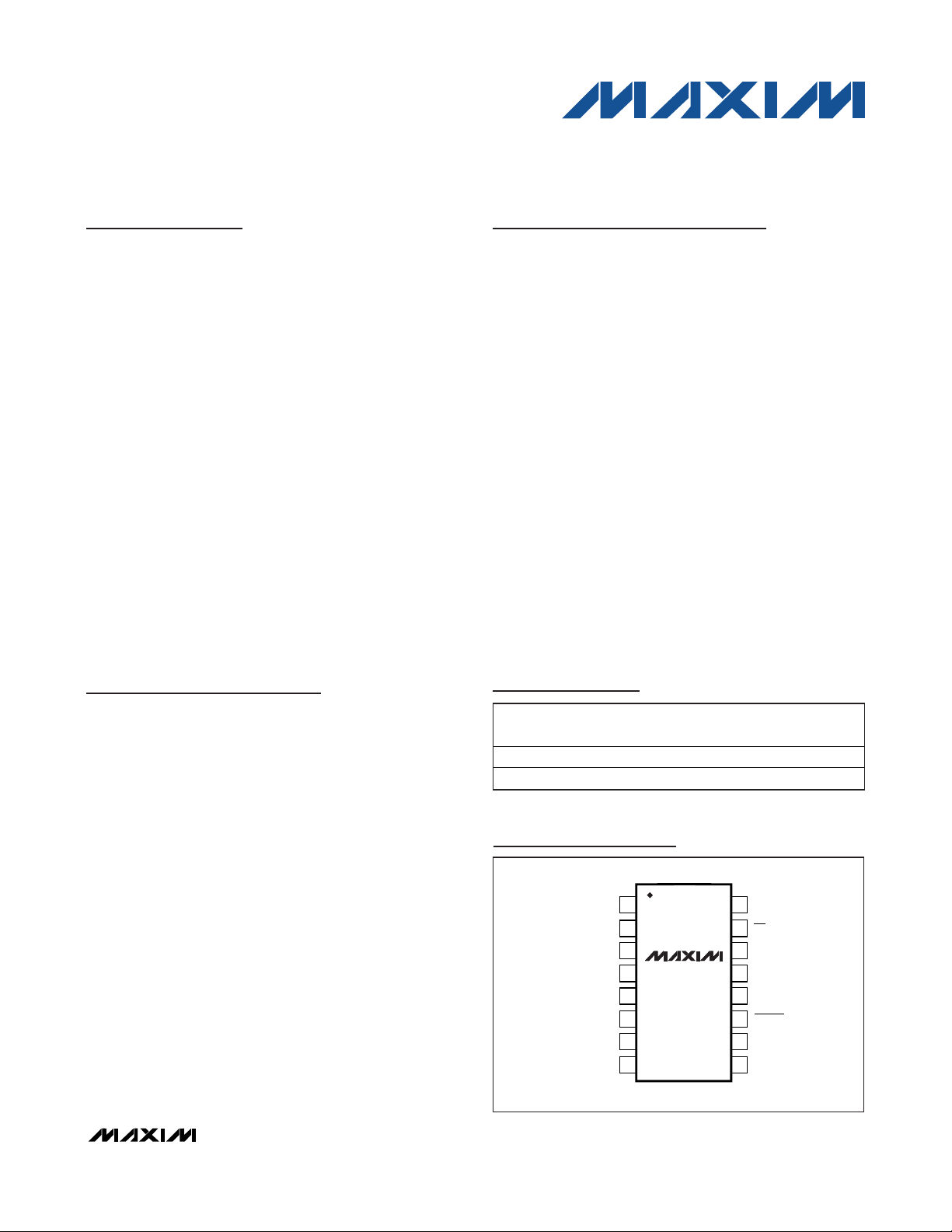
Pin Configuration
19-2436; Rev 2; 1/08
For pricing delivery, and ordering information please contact Maxim Direct at 1-888-629-4642,
or visit Maxim’s website at www.maxim-ic.com.
General Description
The MXB7846 is an industry-standard 4-wire touchscreen controller. It contains a 12-bit sampling analogto-digital converter (ADC) with a synchronous serial
interface and low on-resistance switches for driving
resistive touch screens. The MXB7846 uses an internal
+2.5V reference or an external reference. The
MXB7846 can make absolute or ratiometric measurements. In addition, this device has an on-chip temperature sensor, a battery-monitoring channel, and has the
ability to perform touch-pressure measurements without
external components. The MXB7846 has one auxiliary
ADC input. All analog inputs are fully ESD protected,
eliminating the need for external TransZorb™ devices.
The MXB7846 is guaranteed to operate with a supply
voltage down to +2.375V when used with an external
reference or +2.7V with an internal reference. In shutdown mode, the typical power consumption is reduced
to under 0.5µW, while the typical power consumption at
125ksps throughput and a +2.7V supply is 650µW.
Low-power operation makes the MXB7846 ideal for battery-operated systems, such as personal digital assistants with resistive touch screens and other portable
equipment. The MXB7846 is available in 16-pin QSOP
and TSSOP packages, and is guaranteed over the
-40°C to +85°C temperature range.
Applications
Personal Digital Assistants
Portable Instruments
Point-of-Sales Terminals
Pagers
Touch-Screen Monitors
Cellular Phones
Features
♦ ESD-Protected ADC Inputs
±15kV IEC 61000-4-2 Air-Gap Discharge
±8kV IEC 61000-4-2 Contact Discharge
♦ Pin Compatible with MXB7843
♦ +2.375V to +5.25V Single Supply
♦ Internal +2.5V Reference
♦ Direct Battery Measurement (0 to 6V)
♦ On-Chip Temperature Measurement
♦ Touch-Pressure Measurement
♦ 4-Wire Touch-Screen Interface
♦ Ratiometric Conversion
♦ SPI™/QSPI™, 3-Wire Serial Interface
♦ Programmable 8-/12-Bit Resolution
♦ Auxiliary Analog Input
♦ Automatic Shutdown Between Conversions
♦ Low Power (External Reference)
270µA at 125ksps
115µA at 50ksps
25µA at 10ksps
5µA at 1ksps
2µA Shutdown Current
Ordering Information
TRANSZORB is a trademark of Vishay Intertechnology, Inc.
SPI/QSPI are trademarks of Motorola, Inc.
Typical Application Circuit appears at end of data sheet.
PART TEMP RANGE
MXB7846EEE -40°C to +85°C 16 QSOP E16-6
MXB7846EUE -40°C to +85°C 16 TSSOP U16-1
PINPACKAGE
PKG
CODE
TOP VIEW
V
GND
BAT
AUX
DD
1
X+
2
Y+
3
4
X-
Y-
5
6
7
8
16
DCLK
15
CS
14
DIN
MXB7846
QSOP/TSSOP
13
BUSY
12
DOUT
PENIRQ
11
10
V
DD
REF
9
Page 2
MXB7846
2.375V to 5.25V, 4-Wire Touch-Screen Controller
with Internal Reference and Temperature Sensor
2 _______________________________________________________________________________________
ABSOLUTE MAXIMUM RATINGS
Stresses beyond those listed under “Absolute Maximum Ratings” may cause permanent damage to the device. These are stress ratings only, and functional
operation of the device at these or any other conditions beyond those indicated in the operational sections of the specifications is not implied. Exposure to
absolute maximum rating conditions for extended periods may affect device reliability.
VDD, VBAT, DIN, CS, DCLK to GND ........................-0.3V to +6V
Digital Outputs to GND...............................-0.3V to (V
DD
+ 0.3V)
V
REF
, X+, X-, Y+, Y-, AUX to GND..............-0.3V to (VDD+ 0.3V)
Maximum Current into Any Pin .........................................±50mA
Maximum ESD per IEC-61000-4-2 (per MIL STD-883 HBM)
X+, X-, Y+, Y-, VBAT, AUX ......................................15kV (4kV)
All Other Pins ..........................................................2kV (500V)
Continuous Power Dissipation (T
A
= +70°C)
16-Pin QSOP (derate 8.30mW/°C above +70°C).........667mW
16-Pin TSSOP (derate 5.70mW/°C above +70°C) .......456mW
Operating Temperature Range ...........................-40°C to +85°C
Junction Temperature......................................................+150°C
Storage Temperature Range .............................-65°C to +150°C
Lead Temperature (soldering, 10s) .................................+300°C
ELECTRICAL CHARACTERISTICS
(VDD= 2.7V to 3.6V, V
REF
= 2.5V, f
DCLK
= 2MHz (50% duty cycle), f
SAMPLE
= 125kHz, 12-bit mode, 0.1µF capacitor at REF, TA=
T
MIN
to T
MAX
, unless otherwise noted. Typical values are at TA= +25°C.)
DC ACCURACY (Note 1)
Resolution 12 Bits
No Missing Codes 11 12 Bits
Relative Accuracy INL (Note 2) ±1 ±2 LSB
Differential Nonlinearity DNL ±1 LSB
Offset Error ±6 LSB
Gain Error (Note 3) ±4 LSB
Noise Including internal reference 70 µV
CONVERSION RATE
Conversion Time t
Track/Hold Acquisition Time t
Throughput Rate f
Multiplexer Settling Time 500 ns
Aperture Delay 30 ns
Aperture Jitter 100 p s
Channel-to-Channel Isolation VIN = 2.5V
Serial Clock Frequency f
Duty Cycle 40 60 %
ANALOG INPUT (X+, X-, Y+, Y-, AUX)
Input Voltage Range 0V
Input Capacitance 25 pF
Input Leakage Current On/off leakage, VIN = 0 to V
SWITCH DRIVERS
On-Resistance (Note 5)
INTERNAL REFERENCE
Reference Output Voltage V
REF Output Tempco TCV
REF Short-Circuit Current 18 mA
REF Output Impedance 250 Ω
PARAMETER SYM B O L CONDITIONS MIN TYP MAX UNITS
CONV
ACQ
SAMPLE
DCLK
REF
12 clock cycles (Note 4) 6 µs
3 clock cycles 1.5 µs
16 clock conversion 125 kHz
Y+, X+ 7
Y-, X- 9
VDD = 2.7V to 5.25V, TA = +25°C 2.45 2.50 2.55 V
REF
at 50kHz 100 dB
P-P
DD
0.1 2.0 MHz
REF
±0.1 ±1 µA
50 ppm°/C
RMS
V
Ω
Page 3
MXB7846
2.375V to 5.25V, 4-Wire Touch-Screen Controller
with Internal Reference and Temperature Sensor
_______________________________________________________________________________________ 3
ELECTRICAL CHARACTERISTICS (continued)
(VDD= 2.7V to 3.6V, V
REF
= 2.5V, f
DCLK
= 2MHz (50% duty cycle), f
SAMPLE
= 125kHz, 12-bit mode, 0.1µF capacitor at REF, TA=
T
MIN
to T
MAX
, unless otherwise noted. Typical values are at TA= +25°C.)
PARAMETER SYM B O L CONDITIONS MIN TYP MAX UNITS
EXTERNAL REFERENCE (Internal reference disabled, reference applied to REF)
Reference Input Voltage Range (Note 7) 1 V
DD
V
Input Resistance 1GΩ
Input Current
f
f
f
= 125kHz 13 40
SAMPLE
= 12.5kHz 2.5
SAMPLE
= 0 ±3
DCLK
µA
BATTERY MONITOR (BAT)
Input Voltage Range 06V
Input Resistance During acquisition 10 kΩ
V
= 2.5V ±2
Accuracy
REF
Internal reference ±3
%
TEMPERATURE MEASUREMENT
Resolution
Accuracy
Differential method (Note 8) 1.6 °C
Single-conversion method 0.3 °C
Differential method (Note 8) ±2°C
Single-conversion method ±3°C
DIGITAL INPUTS (DCLK, CS, DIN)
Input High Voltage V
Input Low Voltage V
Input Hysteresis V
Input Leakage Current I
Input Capacitance C
IH
IL
HYST
IN
IN
✕
V
0.7 V
DD
100 mV
15 pF
0.8 V
±1 µA
DIGITAL OUTPUT (DOUT, BUSY)
Output Voltage Low V
Output Voltage High V
PENIRQ Output Low Voltage V
Three-State Leakage Current I
Three-State Output Capacitance C
OUT
OL
OH
OL
L
I
= 250µA 0.4 V
SINK
I
50kΩ pullup to V
CS = V
CS = V
= 250µA V
SOURCE
DD
DD
DD
0.5 V
DD -
1 ±10 µA
15 pF
0.8 V
POWER REQUIREMENTS
Supply Voltage V
Supply Current I
Shutdown Supply Current I
Power-Supply Rejection Ratio P
DD
DD
SHDN
SRR
External reference 2.375 5.250
Internal reference 2.70 5.25
External
reference
Internal
reference
DCLK = CS = V
f
f
f
f
f
f
DD
= 125ksps 270 650
SAMPLE
= 12.5ksps 220
SAMPLE
= 0 150
SAMPLE
= 125ksps 780 950
SAMPLE
= 12.5ksps 720
SAMPLE
= 0 650
SAMPLE
3µA
VDD = 2.7V to 3.6V full scale 70 dB
V
µA
µA
Page 4
MXB7846
2.375V to 5.25V, 4-Wire Touch-Screen Controller
with Internal Reference and Temperature Sensor
4 _______________________________________________________________________________________
Note 1: Tested at VDD= 2.7V.
Note 2: Relative accuracy is the deviation of the analog value at any code from its theoretical value after the full-scale range has
been calibrated.
Note 3: Offset nulled.
Note 4: Conversion time is defined as the number of clock cycles multiplied by the clock period; clock has 50% duty cycle.
Note 5: Resistance measured from the source to drain of the switch.
Note 6: External load should not change during conversion for specified accuracy.
Note 7: ADC performance is limited by the conversion noise floor, typically 300µV
P-P
. An external reference below 2.5V can com-
promise the ADC performance.
Note 8: Difference between Temp0 and Temp1. No calibration necessary.
TIMING CHARACTERISTICS (Figure 1)
(VDD= 2.7V to 3.6V, V
REF
= 2.5V, f
DCLK
= 2MHz (50% duty cycle), f
SAMPLE
= 125kHz, 12-bit mode, 0.1µF capacitor at REF, TA=
T
MIN
to T
MAX
, unless otherwise noted. Typical values are at TA= +25°C.)
TIMING CHARACTERISTICS (Figure 1)
Acquisition Time t
DCLK Clock Period t
DCLK Pulse Width High t
DCLK Pulse Width Low t
DIN-to-DCLK Setup Time t
DIN-to-DCLK Hold Time t
CS Fall-to-DCLK Rise Setup Time t
CS Rise-to-DCLK Rise Ignore t
DCLK Falling-to-DOUT Valid t
CS Rise-to-DOUT Disable t
CS Fall-to-DOUT Enable t
DCLK Falling-to-BUSY Rising t
CS Falling-to-BUSY Enable t
CS Rise-to-BUSY Disable t
PARAMETER SYM B O L CONDITIONS MIN TYP MAX UNITS
ACQ
CP
CH
CL
DS
DH
CSS
CSH
DO
TR
DV
BD
BDV
BTR
C
C
C
LOAD
LOAD
LOAD
= 50pF 200 ns
= 50pF 200 ns
= 50pF 200 ns
1.5 µs
500 ns
200 ns
200 ns
100 ns
0ns
100 ns
0ns
200 ns
200 ns
200 ns
Page 5
Typical Operating Characteristics
(VDD= 2.7V, V
REF
= 2.5V
EXTERNAL
, f
DCLK
= 2MHz, f
SAMPLE
= 125kHz, C
LOAD
= 50pF, 0.1µF capacitor at REF, TA= +25°C, unless
otherwise noted.)
MXB7846
2.375V to 5.25V, 4-Wire Touch-Screen Controller
with Internal Reference and Temperature Sensor
_______________________________________________________________________________________
5
INTEGRAL NONLINEARITY
vs. DIGITAL OUTPUT CODE
0.5
0.4
0.3
0.2
0.1
0
INL (LSB)
-0.1
-0.2
-0.3
-0.4
0 4000
CHANGE IN OFFSET ERROR
1.0
0.5
OUTPUT CODE
vs. TEMPERATURE
350030002000 25001000 1500500
1.0
0.8
MXB7846 toc01
0.6
0.4
0.2
DNL (LSB)
-0.2
-0.4
-0.6
-0.8
-1.0
MXB7846 toc05
DIFFERENTIAL NONLINEARITY
vs. DIGITAL OUTPUT CODE
0
0 4000
OUTPUT CODE
CHANGE IN GAIN ERROR
vs. SUPPLY VOLTAGE
3
2
1
350030002000 25001000 1500500
MXB7846 toc02
OFFSET ERROR (LSB)
MXB7846 toc07
CHANGE IN OFFSET ERROR
vs. SUPPLY VOLTAGE
2.0
1.5
1.0
0.5
0
-0.5
-1.0
-1.5
-2.0
2.5 5.5
SUPPLY VOLTAGE (V)
CHANGE IN GAIN ERROR
vs. TEMPERATURE
1.0
0.5
0
MXB7846 toc04
5.04.53.0 3.5 4.0
MXB7846 toc08
0
-0.5
OFFSET ERROR FROM +25°C (LSB)
-1.0
-40 80
655035205-10-25
°
SWITCH ON-RESISTANCE vs. SUPPLY VOLTAGE
(X+, Y+ : +V
14
12
10
8
(Ω)
ON
R
6
4
2
0
2.5 5.5
TO PIN; X-, Y- : TO GND)
DD
X-
Y-
X+
Y+
SUPPLY VOLTAGE (V)
5.04.54.03.53.0
GAIN ERROR (LSB)
MXB7846 toc03
(Ω)
ON
R
0
-1
-2
-3
2.5 5.5
SUPPLY VOLTAGE (V)
5.04.54.03.53.0
SWITCH ON-RESISTANCE vs. TEMPERATURE
(X+, Y+ : +V
12
11
10
9
8
7
6
5
4
3
2
1
0
-40 50 65 80
TO PIN; X-, Y- : PIN TO GND)
DD
X-
X+
Y-
Y+
35205-10-25
TEMPERATURE (°C)
-0.5
-1.0
GAIN ERROR FROM +25°C (LSB)
-1.5
-2.0
2.6
2.5
MXB7846 toc06
2.4
2.3
2.2
INTERNAL REFERENCE (V)
2.1
2.0
-40 80
655035205-10-25
°
INTERNAL REFERENCE
vs. SUPPLY VOLTAGE
CL = 0.1μf
2.0 5.5
SUPPLY VOLTAGE (V)
5.04.54.03.53.02.5
MXB7846 toc09
Page 6
Typical Operating Characteristics (continued)
(VDD= 2.7V, V
REF
= 2.5V
EXTERNAL
, f
DCLK
= 2MHz, f
SAMPLE
= 125kHz, C
LOAD
= 50pF, 0.1µF capacitor at REF, TA= +25°C, unless
otherwise noted.)
MXB7846
2.375V to 5.25V, 4-Wire Touch-Screen Controller
with Internal Reference and Temperature Sensor
6 _______________________________________________________________________________________
2.6
INTERNAL REFERENCE VOLTAGE
vs. TEMPERATURE
2.5
INTERNAL VOLTAGE REFERENCE
vs. TURN-ON TIME
INTERNAL VOLTAGE REFERENCE
vs. TURN-ON TIME
3.0
2.5
2.4
2.3
2.2
INTERNAL REFERENCE VOLTAGE (V)
2.1
VDD = 2.7V
= 0.1μF
C
L
2.0
-40
TEMPERATURE (°C)
REFERENCE CURRENT
vs. SUPPLY VOLTAGE
8.3
CL = 0.1μF
= 125kHz
f
SAMPLE
8.2
EXTERNAL REFERENCE
8.1
8.0
7.9
REFERENCE CURRENT (μA)
7.8
7.7
2.5 5.5
SUPPLY VOLTAGE (V)
TEMP DIODE VOLTAGE
vs. TEMPERATURE
1.0
0.9
0.8
0.7
0.6
0.5
0.4
0.3
TEMP DIODE VOLTAGE (V)
0.2
0.1
0
-40
TEMP2
TEMPERATURE (°C)
TEMP1
MXB7846 toc10
2.0
1.5
1.0
0.5
INTERNAL VOLTAGE REFERENCE (V)
80655035205-10-25
0
0
(1060μs) 12-BIT SETTLING
TURN-ON TIME (μs)
CL = 1μF
12001000800600400200
REFERENCE CURRENT vs. TEMPERATURE
8.3
8.2
MXB7846 toc12
8.1
8.0
7.9
REFERENCE CURRENT (μA)
VDD = 2.7V
= 0.1μF
C
L
7.8
5.04.54.03.53.0
7.7
= 125kHz
f
SAMPLE
EXTERNAL REFERENCE
-40 80
TEMPERATURE (°C)
655035205-10-25
TEMP0 DIODE VOLTAGE
vs. SUPPLY VOLTAGE
590
MXB7846 toc15
589
TEMP0
588
587
TEMP0 DIODE VOLTAGE (mV)
586
585
806535 50-10 5 20-25
2.7
SUPPLY VOLTAGE (V)
5.24.74.23.73.2
2.5
MXB7846 toc11a
2.0
1.5
1.0
INTERNAL VOLTAGE REFERENCE (V)
0.5
0
040
REFERENCE CURRENT vs. SAMPLE RATE
10
EXTERNAL REFERENCE
9
MXB7846 toc13
MXB7846 toc16
8
7
6
5
4
3
REFERENCE CURRENT (μA)
2
1
0
0 125
705
704
703
702
701
700
TEMP1 DIODE VOLTAGE (mV)
699
698
2.7
NO CAPACITOR
(30μs) 12-BIT SETTLING
TURN-ON TIME (μs)
SAMPLE RATE (kHz)
TEMP1 DIODE VOLTAGE
vs. SUPPLY VOLTAGE
TEMP1
SUPPLY VOLTAGE (V)
MXB7846 toc11b
3530252015105
MXB7846 toc14
100755025
MXB7846 toc17
5.24.74.23.73.2
Page 7
Typical Operating Characteristics (continued)
(VDD= 2.7V, V
REF
= 2.5V
EXTERNAL
, f
DCLK
= 2MHz, f
SAMPLE
= 125kHz, C
LOAD
= 50pF, 0.1µF capacitor at REF, TA= +25°C, unless
otherwise noted.)
MXB7846
2.375V to 5.25V, 4-Wire Touch-Screen Controller
with Internal Reference and Temperature Sensor
_______________________________________________________________________________________
7
SUPPLY CURRENT
vs. SUPPLY VOLTAGE
250
f
= 12.5kHz
SAMPLE
225
200
SUPPLY CURRENT (μA)
175
150
2.0 5.5
SUPPLY VOLTAGE (V)
SHUTDOWN CURRENT
vs. SUPPLY VOLTAGE
300
DCLK = CS = V
250
200
DD
5.04.54.03.53.02.5
MXB7846 toc18
SUPPLY CURRENT (μA)
MXB7846 toc21
290
285
280
275
270
265
260
255
250
-40 80
SHUTDOWN CURRENT vs. TEMPERATURE
120
110
100
90
SUPPLY CURRENT vs. TEMPERATURE
f
= 125kHz
SAMPLE
= 2.7V
V
DD
6550-25 -10 5 20 35
TEMPERATURE (°C)
DCLK = CS = VDD = 3V
MXB7846 toc19
MXB7846 toc22
SUPPLY CURRENT vs. SAMPLE RATE
250
VDD = 2.7V
= 2.5V
V
REF
225
200
175
150
SUPPLY CURRENT (μA)
125
100
0 125
SAMPLE RATE (kHz)
MAXIMUM SAMPLE RATE
vs. SUPPLY VOLTAGE
1000
100
MXB7846 toc20
100755025
MXB7846 toc23
150
SHUTDOWN CURRENT (nA)
100
50
2.7 5.2
SUPPLY VOLTAGE (V)
80
SAMPLE RATE (kHz)
70
SHUTDOWN CURRENT (nA)
60
4.74.23.73.2
50
-40 80
TEMPERATURE (°C)
655035205-10-25
10
1
2.0 5.5
SUPPLY VOLTAGE (V)
5.04.54.03.53.02.5
Page 8
Pin Description
MXB7846
2.375V to 5.25V, 4-Wire Touch-Screen Controller
with Internal Reference and Temperature Sensor
8 _______________________________________________________________________________________
Figure 1. Detailed Serial Interface Timing
PIN NAME FUNCTION
1VDDPositive Supply Voltage. Connect to pin 10.
2 X+ X+ Position Input, ADC Input Channel 1
3 Y+ Y+ Position Input, ADC Input Channel 2
4 X- X- Position Input
5 Y- Y- Position Input
6 GND Ground
7 BAT Battery Monitoring Inputs; ADC Input Channel 3
8 AUX Auxiliary Input to ADC; ADC Input Channel 4
Voltage Reference Output/Input. Reference voltage for analog-to-digital conversion. In internal
9 REF
10 V
DD
reference mode, the reference buffer provides a 2.50V nominal output. In external reference mode,
apply a reference voltage between 1V and V
. Bypass REF to GND with a 0.1µF capacitor.
DD
Positive Supply Voltage, +2.375V (2.70V) to +5.25V. External (internal) reference. Bypass with a 1µF
capacitor. Connect to pin 1.
11 PENIRQ Pen Interrupt Output. Open anode output. 10kΩ to 100kΩ pullup resistor required to VDD.
12 DOUT
13 BUSY
Serial Data Output. Data changes state on the falling edge of DCLK. High impedance when CS is
HIGH.
Busy Output. BUSY pulses high for one clock period before the MSB decision. High impedance when
CS is HIGH.
14 DIN Serial Data Input. Data clocked in on the rising edge of DCLK.
15 CS
16 DCLK
Active-Low Chip Select. Data is only clocked into DIN when CS is low. When CS is HIGH, DOUT and
BUSY are high impedance.
Serial Clock Input. Clocks data in and out of the serial interface and sets the conversion speed (duty
cycle must be 40% to 60%).
CS
t
DCLK
DIN
DOUT
BUSY
t
CSS
t
DS
t
DH
t
DV
t
BDV
CH
t
CL
t
CP
t
DO
t
BD
t
CSH
t
TR
t
BTR
Page 9

MXB7846
2.375V to 5.25V, 4-Wire Touch-Screen Controller
with Internal Reference and Temperature Sensor
_______________________________________________________________________________________ 9
Detailed Description
The MXB7846 uses a successive-approximation conversion technique to convert analog signals to a 12-bit digital output. An SPI/QSPI/MICROWIRE™-compatible serial
interface provides easy communication to a microprocessor (µP). It features an internal 2.5V reference, an
on-chip temperature sensor, a battery monitor, and a
4-wire touch-screen interface (
Functional Diagram
).
Analog Inputs
Figure 2 shows a block diagram of the analog input section that includes the input multiplexer of the MXB7846,
the differential signal inputs of the ADC, and the differential reference inputs of the ADC. The input multiplexer
switches between X+, X-, Y+, Y-, AUX, BAT, and the
internal temperature sensor.
In single-ended mode, conversions are performed using
REF as the reference. In differential mode, ratiometric
conversions are performed with REF+ connected to X+ or
Y+, and REF- connected to X- or Y-. Configure the reference and switching matrix according to Tables 1 and 2.
During the acquisition interval, the selected channel
charges the sampling capacitance. The acquisition
interval starts on the fifth falling clock edge and ends
on the eighth falling clock edge.
The time required for the T/H to acquire an input signal
is a function of how quickly its input capacitance is
charged. If the input signal’s source impedance is high,
the acquisition time lengthens, and more time must be
allowed between conversions. The acquisition time
(t
ACQ
) is the maximum time the device takes to acquire
the input signal to 12-bit accuracy. Calculate t
ACQ
with
the following equation:
where RIN= 2kΩ and RSis the source impedance of
the input signal.
Source impedances below 1kΩ do not significantly affect
the ADC’s performance. Accommodate higher source
impedances by either slowing down DCLK or by placing
a 1µF capacitor between the analog input and GND.
tRRpF
ACQ S IN
. =× +
()
×84 25
MICROWIRE is a trademark of National Semiconductor Corp.
Figure 2. Equivalent Input Circuit
PENIRQ
TEMP0
TEMP1
+V
V
DD
REF
X+
X-
Y+
Y-
V
AUX
GND
BAT
7.5kΩ
2.5kΩ
BATTERY
MXB7846
A2–A0
)
(SHOWN 001
B
2.5V
REFERENCE
ON
SER/DFR
(SHOWN HIGH)
REF ON/OFF
+IN
12-BIT ADC
-IN
REF+
REF-
Page 10

MXB7846
2.375V to 5.25V, 4-Wire Touch-Screen Controller
with Internal Reference and Temperature Sensor
10 ______________________________________________________________________________________
Functional Diagram
Table 1. Input Configuration, Single-Ended Reference Mode (SER/DFR HIGH)
Table 2. Input Configuration, Differential Reference Mode (SER/DFR LOW)
V
DD
PENIRQ
X+
X-
TEMPERATURE
SENSOR
DOUT
BUSY
PENIRQ
DCLK
DIN
CS
BAT
AUX
REF
Y+
Y-
BATTERY
MONITOR
6-TO-1
MUX
12-BIT ADC
SERIAL
DATA
INTERFACE
2.5V
REFERENCE
A2 A1 A0 MEASUREMENT ADC INPUT CONNECTION DRIVERS ON
0 0 0 Temp0 Temp0 —
0 0 1 Y position X+ Y+, Y-
0 1 0 BAT BAT —
0 1 1 Z1 X+ X-, Y+
1 0 0 Z2 Y- X-, Y+
1 0 1 X- position Y+ X-, X+
1 1 0 AUX AUX —
1 1 1 Temp1 Temp1 —
A2 A1 A0
ADC +REF
CONNECTION TO
0 0 1 Y+ Y- X+ Y position Y+, Y-
0 1 1 Y+ X- X+ Z1 position Y+, X-
1 0 0 Y+ X- Y- Z2 position Y+, X-
1 0 1 X+ X- Y+ X position X+, X-
ADC -REF
CONNECTION TO
ADC INPUT
CONNECTION TO
MEASUREMENT
PERFORMED
DRIVER ON
Page 11

MXB7846
2.375V to 5.25V, 4-Wire Touch-Screen Controller
with Internal Reference and Temperature Sensor
______________________________________________________________________________________ 11
Input Bandwidth and Anti-Aliasing
The ADCs input tracking circuitry has a 25MHz smallsignal bandwidth, so it is possible to digitize highspeed transient events. To avoid high-frequency signals being aliased into the frequency band of interest,
anti-alias filtering is recommended.
Analog Input Protection
Internal protection diodes, which clamp the analog input
to VDDand GND, allow the analog input pins to swing
from GND - 0.3V to V
DD
+ 0.3V without damage. Analog
inputs must not exceed VDDby more than 50mV or be
lower than GND by more than 50mV for accurate conversion. If an off-channel analog input voltage exceeds
the supplies, limit the input current to 50mA. The analog
input pins are ESD protected to ±8kV using the Contact
Discharge method and ±15kV using the Air-Gap
method specified in IEC 61000-4-2.
Touch-Screen Conversion
The MXB7846 provides two conversion methods—differential and single ended. The SER/DFR bit in the control
word selects either mode. A logic 1 selects a singleended conversion, while a logic 0 selects a differential
conversion.
Differential vs. Single Ended
Changes in operating conditions can degrade the accuracy and repeatability of touch-screen measurements.
Therefore, the conversion results representing X and Y
coordinates may be incorrect. For example, in singleended measurement mode, variation in the touch-screen
driver voltage drops results in incorrect input reading.
Differential mode minimizes these errors.
Single-Ended Mode
Figure 3 shows the switching matrix configuration for
Y-coordinate measurement in single-ended mode. The
MXB7846 measures the position of the pointing device
by connecting X+ to IN+ of the ADC, enabling Y+ and
Y- drivers, and digitizing the voltage on X+. The ADC
performs a conversion with REF+ = REF and REF- =
GND. In single-ended measurement mode, the bias to
the touch screen can be turned off after the acquisition
to save power. The on-resistance of the X and Y drivers
results in a gain error in single-ended measurement
mode. Touch-screen resistance ranges from 200Ω to
900Ω (depending on the manufacturer), whereas the
on-resistance of the X and Y drivers is 8Ω (typ). Limit
the touch-screen current to less than 50mA by using a
touch screen with a resistance higher than 100Ω. The
resistive-divider created by the touch screen and the
on-resistance of the X and Y drivers result in both an
offset and a gain shift. Also, the on-resistance of the X
and Y drivers does not track the resistance of the touch
screen over temperature and supply. This results in further measurement errors.
Differential Measurement Mode
Figure 4 shows the switching matrix configuration for
Y-coordinate measurement. The REF+ and REF- inputs
are connected directly to the Y+ and Y- pins, respectively. Differential mode uses the voltage at the Y+ pin
as the REF+ voltage and voltage at the Y- pin as REFvoltage. This conversion is ratiometric and independent
of the voltage drop across the drivers and variation in
the touch-screen resistance. In differential mode, the
touch screen remains biased during the acquisition and
conversion process. This results in additional supply
current and power dissipation during conversion when
compared to the absolute measurement mode.
PEN Interrupt Request (PENIRQ)
Figure 5 shows the block diagram for the PENIRQ function. When used, PENIRQ requires a 10kΩ to 100kΩ
pullup to +VDD. If enabled, PENIRQ goes low whenever
the touch screen is touched. The PENIRQ output can
be used to initiate an interrupt to the microprocessor,
which can write a control word to the MXB7846 to start
a conversion.
Figure 6 shows the timing diagram for the PENIRQ pin
function. The diagram shows that once the screen is
touched while CS is high, the PENIRQ output goes low
after a time period indicated by t
TOUCH
. The t
TOUCH
value changes for different touch-screen parasitic
capacitance and resistance. The microprocessor
receives this interrupt and pulls CS low to initiate a conversion. At this instant, the PENIRQ pin should be
masked, as transitions can occur due to a selected
input channel or the conversion mode. The PENIRQ pin
functionality becomes valid when either the last data bit
is clocked out, or CS is pulled high.
Touch-Pressure Measurement
The MXB7846 provides two methods for measuring the
pressure applied to the touch screen (Figure 7). By
measuring R
TOUCH
, it is possible to differentiate
between a finger or stylus in contact with the touch
screen. Although 8-bit resolution is typically sufficient,
the following calculations use 12-bit resolution demonstrating the maximum precision of the MXB7846.
Page 12

MXB7846
2.375V to 5.25V, 4-Wire Touch-Screen Controller
with Internal Reference and Temperature Sensor
12 ______________________________________________________________________________________
Figure 3. Single-Ended Y-Coordinate Measurement
Figure 4. Ratiometric Y-Coordinate Measurement
Figure 5. PENIRQ Functional Block Diagram
V
DD
V
DD
Y+
X+
Y-
GND
+IN
-IN
REF
REF+
12-BIT ADC
REF-
Y+
REF+
X+
Y-
GND
+IN
12-BIT ADC
-IN
REF-
+V
DD
100kΩ
PENIRQ
TOUCH SCREEN
OPEN CIRCUIT
Y+
X+
Y-
ON
PENIRQ
ENABLE
Page 13

MXB7846
2.375V to 5.25V, 4-Wire Touch-Screen Controller
with Internal Reference and Temperature Sensor
______________________________________________________________________________________ 13
The first method performs pressure measurements
using a known X-plate resistance. After completing
three conversions (X-position, Z1, and Z2), use the following equation to calculate R
TOUCH
:
The second method requires knowing both the X-plate
and Y-plate resistance. Three conversions are required in
this method: the X-position, Y-position, and Z1-position.
Use the following equation to calculate R
TOUCH:
Internal Temperature Sensor
The MXB7846 provides two temperature measurement
options: single-ended conversion and differential conversion. Both temperature measurement techniques rely
on the semiconductor junction’s temperature characteristics. The forward diode voltage (VBE) vs. temperature
is a well-defined characteristic. The ambient temperature can be calculated by knowing the value of VBEat a
fixed temperature and then monitoring the change in
that voltage as the temperature changes. The single
conversion method requires calibration at a known temperature, but only needs a single reading to calculate
R
R
Z
X
Z
R
Y
TOUCH
XPLATE POSITION
YPLATE
POSITION
=
⎛
⎝
⎜
⎞
⎠
⎟
×
⎛
⎝
⎜
⎞
⎠
⎟
×
⎛
⎝
⎜
⎞
⎠
⎟
⎡
⎣
⎢
⎢
⎧
⎨
⎪
⎩
⎪
×
⎛
⎝
⎜
⎞
⎠
⎟
⎧
⎨
⎩
⎫
⎬
⎭
−
−
11
4096
4096
1
4096
RR
XZ
Z
TOUCH XPLATE
POSITION
=
()
×
⎛
⎝
⎜
⎞
⎠
⎟
×
⎛
⎝
⎜
⎞
⎠
⎟
⎡
⎣
⎢
⎢
⎤
⎦
⎥
⎥
−
4096
1
2
1
Figure 7. Pressure Measurement Block Diagram
Figure 6. PENIRQ Timing Diagram
SCREEN TOUCHED HERE
PENIRQ
CS
DCLK
DIN
+
V
-
MEASURE Z1
1 2 3 4 5 6 7 8 1 2 3 1213141516
S A2 A1 A0 M S/D PD1 PD0
INTERRUPT PROCESSOR
t
TOUCH
X+
R
TOUCH
FORCED LINE
X- POSITION
X-
X+
OPEN CIRCUIT
Y+
NO RESPONSE TO TOUCH⎯MASK PENIRQ
MEASURE X- POSITION
Y+
SENSE LINE
Y-
PENIRQ ENABLED
R
SENSE LINE
X-
OPEN CIRCUIT
X+
TOUCH
OPEN CIRCUIT
Y-
Y+
+
V
-
FORCED LINE
R
TOUCH
+
V
-
X-
FORCED LINE
Y-
SENSE LINE
MEASURE Z2
Page 14

MXB7846
2.375V to 5.25V, 4-Wire Touch-Screen Controller
with Internal Reference and Temperature Sensor
14 ______________________________________________________________________________________
the ambient temperature. First, the PENIRQ diode forward bias voltage is measured by the ADC with an
address of A2 = 0, A1 = 0, and A0 = 0 at a known temperature. Subsequent diode measurements provide an
estimate of the ambient temperature through extrapolation. This assumes a temperature coefficient of
-2.1mV/°C. The single conversion method results in a
resolution of 0.3°C/LSB and a typical accuracy of ±3°C.
The differential conversion method uses two measurement points. The first measurement (Temp0) is performed with a fixed bias current into the PENIRQ diode.
The second measurement (Temp1) is performed with a
fixed multiple of the original bias current with an
address of A2 = 1, A1 = 1, and A0 = 1. The voltage difference between the first and second conversion is
proportional to the absolute temperature and is
expressed by the following formula:
where T0 (Temp0) and T1 (Temp1) are the conversion
results.
This differential conversion method can provide much
improved absolute temperature measurement; however,
the resolution is reduced to 1.6°C/LSB.
Battery Voltage Monitor
A dedicated analog input (BAT) allows the MXB7846 to
monitor the system battery voltage. Figure 8 shows the
battery voltage monitoring circuitry. The MXB7846 monitors battery voltages from 0 to 6V. An internal resistor
network divides down V
BAT
by 4 so that a 6.0V battery
voltage results in 1.5V at the ADC input. To minimize
power consumption, the divider is only enabled during
the sampling of V
BAT
.
Internal Reference
Enable the internal 2.5V reference by setting PD1 in the
control byte to a logic 1 (see Tables 3 and 4). The
MXB7846 uses the internal reference for single-ended
measurement mode, battery monitoring, temperature
measurement, and for measurement on the auxiliary
input. To minimize power consumption, disable the internal reference by setting PD1 to a logic 0 when performing
ratiometric position measurements. The internal 2.5V reference typically requires 10ms to settle (with no external
load). For optimum performance, connect a 0.1µF capacitor from REF to GND. This internal reference can be overdriven with an external reference. For best performance,
the internal reference should be disabled when the external reference is applied. The internal reference of the
MXB7846 must also be disabled to maintain compatibility
with the MXB7843. To disable the internal reference of the
MXB7846 after power-up, a control byte with PD1 = 0 is
required. (See
Typical Operating Characteristics
for
power-up time of the reference from power down.)
External Reference
Although the internal reference may be overdriven with
an external reference, the internal reference should be
disabled (PD1 = 0) for best performance when using
an external reference. During conversion, an external
reference at REF must deliver up to 40µA DC load current. If the reference has a higher output impedance or
is noisy, bypass it close to the REF pin with a 0.1µF and
a 4.7µF capacitor. Temperature measurements are
always performed using the internal reference.
Digital Interface
Initialization After Power-Up and Starting a
Conversion
The digital interface consists of three inputs, DIN, DCLK,
CS, and one output, DOUT. A logic-high on CS disables
the MXB7846 digital interface and places DOUT in a
high-impedance state. Pulling CS low enables the
MXB7846 digital interface.
TC T T
VREF
() . ( )°= ×
⎛
⎝
⎜
⎞
⎠
⎟
×
⎡
⎣
⎢
⎤
⎦
⎥
−−260 1 0
4096
1000 273
Figure 8. Battery Measurement Functional Block Diagram
BATTERY
0 TO 6.0V
7.5kΩ
BAT
2.5kΩ
DC/DC
CONVERTER
0 TO 1.5V
+2.375V TO +5.25V
V
DD
12-BIT ADC
BATTERY
MEASUREMENT ON
Page 15

MXB7846
2.375V to 5.25V, 4-Wire Touch-Screen Controller
with Internal Reference and Temperature Sensor
______________________________________________________________________________________ 15
Start a conversion by clocking a control byte into DIN
(Table 3) with CS low. Each rising edge on DCLK
clocks a bit from DIN into the MXB7846’s internal shift
register. After CS falls, the first arriving logic 1 bit
defines the control byte’s START bit. Until the START bit
arrives, any number of logic 0 bits can be clocked into
DIN with no effect.
The MXB7846 is compatible with SPI/QSPI/MICROWIRE
devices. For SPI, select the correct clock polarity and
sampling edge in the SPI control registers of the microcontroller: set CPOL = 0 and CPHA = 0. MICROWIRE,
SPI, and QSPI all transmit a byte and receive a byte at
the same time. The simplest software interface requires
only three 8-bit transfers to perform a conversion (one 8bit transfer to configure the ADC, and two more 8-bit
transfers to read the conversion result; Figure 9).
Simple Software Interface
Make sure the CPU’s serial interface runs in master
mode so the CPU generates the serial clock. Choose a
clock frequency from 500kHz to 2MHz:
1) Set up the control byte and call it TB. TB should be
in the format: 1XXXXXXX binary, where X denotes
the particular channel, selected conversion mode,
and power mode (Tables 3, 4).
2) Use a general-purpose I/O line on the CPU to pull
CS low.
3) Transmit TB and simultaneously receive a byte; call
it RB1.
4) Transmit a byte of all zeros ($00 hex) and simultaneously receive byte RB2.
5) Transmit a byte of all zeros ($00 hex) and simultaneously receive byte RB3.
6) Pull CS high.
Figure 9 shows the timing for this sequence. Byte RB2
and RB3 contain the result of the conversion, padded
with four trailing zeros. The total conversion time is a
function of the serial-clock frequency and the amount of
idle timing between 8-bit transfers.
Digital Output
The MXB7846 outputs data in straight binary format. Data
is clocked out on the falling edge of the DCLK MSB first.
Serial Clock
The external clock not only shifts data in and out, but it
also drives the analog-to-digital conversion steps.
BUSY pulses high for one clock period after the last bit
of the control byte. Successive-approximation bit decisions are made and appear at DOUT on each of the
next 12 DCLK falling edges. BUSY and DOUT go into a
high-impedance state when CS goes high.
The conversion must complete in 500µs or less; if not,
droop on the sample-and-hold capacitors can degrade
conversion results.
Data Framing
The falling edge of CS does not start a conversion. The
first logic high clocked into DIN is interpreted as a start
bit and defines the first bit of the control byte. A conversion starts on DCLK’s falling edge, after the eighth bit of
the control byte is clocked into DIN.
The first logic 1 clocked into DIN after bit 6 of a conversion in progress is clocked onto the DOUT pin and is
treated as a START bit (Figure 10).
Once a start bit has been recognized, the current conversion must be completed.
Table 3. Control Byte Format
BIT 7 BIT 6 BIT 5 BIT 4 BIT 3 BIT 2 BIT 1 BIT 0
START A2 A1 A0 MODE SER/DFR PD1 PD0
BIT NAME DESCRIPTION
7 START Start bit
6A2
5A1
4A0
3 MODE Conversion resolution: 1 = 8 bits, 0 = 12 bits
2 SER/DFR Conversion mode: 1 = single ended, 0 = differential
1 PD1
0 PD0
Address (Tables 1 and 2)
Power-down mode (Table 4)
Page 16

MXB7846
2.375V to 5.25V, 4-Wire Touch-Screen Controller
with Internal Reference and Temperature Sensor
16 ______________________________________________________________________________________
The fastest the MXB7846 can run with CS held continuously low is 15 clock conversions. Figure 10 shows the
serial-interface timing necessary to perform a conversion every 15 DCLK cycles. If CS is connected low and
DCLK is continuous, guarantee a start bit by first clocking in 16 zeros.
Most microcontrollers (µCs) require that data transfers
occur in multiples of eight DCLK cycles; 16 clocks per
conversion is typically the fastest that a µC can drive the
MXB7846. Figure 11 shows the serial interface timing necessary to perform a conversion every 16 DCLK cycles.
8-Bit Conversion
The MXB7846 provides an 8-bit conversion mode
selected by setting the MODE bit in the control byte
high. In the 8-bit mode, conversions complete four
clock cycles earlier than in the 12-bit output mode,
resulting in 25% faster throughput. This can be used in
conjunction with serial interfaces that provide 12-bit
transfers, or two conversions could be accomplished
with three 8-bit transfers. Not only does this shorten each
conversion by 4 bits, but each conversion can also
occur at a faster clock rate since settling to better than 8
bits is all that is required. The clock rate can be as much
as 25% faster. The faster clock rate and fewer clock
cycles combine to increase the conversion rate.
Table 4. Power-Mode Selection
Figure 9. Conversion Timing, 24-Clock per Conversion, 8-Bit Bus Interface
SUPPLY CURRENT (typ) (µA)
PD1 PD0 PENIRQ STATUS
0 0 Enabled ADC is ON during conversion, OFF between conversion 200 1
0 1 Disabled ADC is always ON, reference is always OFF 200 200
1 0 Disabled ADC is always OFF, reference is always ON 400 400
1 1 Disabled ADC is always ON, reference is always ON 600 600
CS
T
B
t
ACQ
R
B2
DURING
CONVERSION
R
B3
AFTER
CONVERSION
DCLK
DIN
BUSY
DOUT
A/D STATE
1891216
SA2A1A0
(START)
DRIVERS 1 AND 2
(SER/DFR HIGH)
DRIVERS 1 AND 2
(SER/DFR LOW)
IDLE
SER/
MODE
PD1 PD0
DFR
ACQUIRE CONVERSION IDLE
RB1
(MSB) (LSB)
ACQUIRE
OFF
OFF OFFON
ON OFF
4567891011 3210
CONVERSION
20 244
IDLEIDLE
Page 17

MXB7846
2.375V to 5.25V, 4-Wire Touch-Screen Controller
with Internal Reference and Temperature Sensor
______________________________________________________________________________________ 17
Data Format
The MXB7846 output data is in straight binary format as
shown in Figure 12. This figure shows the ideal output
code for the given input voltage and does not include
the effects of offset, gain, or noise.
Applications Information
Basic Operation of the MXB7846
The 4-wire touch-screen controller works by creating a
voltage gradient across the vertical or horizontal resistive network connected to the MXB7846, as shown in
the
Typical Application Circuit
. The touch screen is
biased through internal MOSFET switches that connect
each resistive layer to VDDand ground on an alternate
basis. For example, to measure the Y position when a
pointing device presses on the touch screen, the Y+
and Y- drivers are turned on, connecting one side of
the vertical resistive layer to V
DD
and the other side to
ground. In this case, the horizontal resistive layer functions as a sense line. One side of this resistive layer
gets connected to the X+ input, while the other side is
left open or floating. The point where the touch screen
is pressed brings the two resistive layers in contact and
forms a voltage-divider at that point. The data converter
senses the voltage at the point of contact through the
X+ input and digitizes it. The horizontal layer resistance
does not introduce any error in the conversion because
no DC current is drawn.
The conversion process of the analog input voltage to
digital output is controlled through the serial interface
between the A/D converter and the µP. The processor
controls the MXB7846 configuration through a control
Figure 11. 16-Clock/Conversion Timing
Figure 10. 15-Clock/Conversion Timing
CS
1 8 15 1 8 15 1
DCLK
DIN
S CONTROL BYTE 0 CONTROL BYTE 1 CONTROL BYTE 2SS
DOUT
BUSY
CS
1 8 16 1 8 16
DCLK
DIN
DOUT
BUSY
CONTROL BYTE 0 CONTROL BYTE 1SS
B11 B10 B9 B8 B7 B6 B5 B4 B3 B2 B1 B0
CONVERSION RESULT 0 CONVERSION RESULT 1
CONVERSION RESULT 0 CONVERSION RESULT 1
B11 B10 B9 B8 B7 B6 B5 B4 B3 B2 B1 B0
B11 B10 B9 B8 B7 B6B11 B10 B9 B8 B7 B6 B5 B4 B3 B2 B1 B0
. . .
. . .
. . .
. . .
. . .
Page 18

MXB7846
2.375V to 5.25V, 4-Wire Touch-Screen Controller
with Internal Reference and Temperature Sensor
18 ______________________________________________________________________________________
byte (see Tables 3 and 4). Once the processor instructs
the MXB7846 to initiate a conversion, the MXB7846
biases the touch screen through the internal switches at
the beginning of the acquisition period. The voltage
transient at the touch screen needs to settle down to a
stable voltage before the acquisition period is over.
After the acquisition period is over, the A/D converter
goes into a conversion period with all internal switches
turned off if the device is in single-ended mode. If the
device is in differential mode, the internal switches
remain on from the start of the acquisition period to the
end of the conversion period.
Power-On Reset
When power is first applied, internal power-on circuitry
resets the MXB7846. Allow 10µs for the first conversion
after the power supplies stabilize. If CS is low, the first
logic 1 on DIN is interpreted as a start bit. Until a conversion takes place, DOUT shifts out zeros. On powerup, allow time for the reference to stabilize.
Power Modes
Save power by placing the converter in one of two lowcurrent operating modes or in full power down between
conversions. Select the power-down mode through
PD1 and PD0 of the control byte (Tables 3 and 4).
The software power-down modes take effect after the
conversion is completed. The serial interface remains
active while waiting for a new control byte to start a conversion and switches to full-power mode. After complet-
ing its conversion, the MXB7846 enters the programmed
power mode until a new control byte is received.
The power-up wait before conversion period is dependent on the power-down state. When exiting software
low-power modes, conversion can start immediately
when running at decreased clock rates. Upon poweron reset, the MXB7846 is in power-down mode with
PD1 = 0 and PD0 = 0. When exiting software shutdown,
the MXB7846 is ready to perform a conversion in 10µs
with an external reference. When using the internal reference, allow enough time for reference to settle to 12bit accuracy when exiting full power-down mode, as
shown in the
Typical Operating Characteristics
.
PD1 = 1, PD0 = 1
In this mode, the MXB7846 is always powered up and
both the reference and the ADC are always on. The
device remains fully powered after the current conversion completes.
PD1 = 0, PD0 = 0
In this mode, the MXB7846 powers down after the current conversion completes or on the next rising edge of
CS, whichever occurs first. The next control byte
received on DIN powers up the MXB7846. At the start
of a new conversion, it instantly powers up. When each
conversion is finished, the part enters power-down
mode, unless otherwise indicated. The first conversion
after the ADC returns to full power is valid for differential conversions and single-ended measurement conversions when using an external reference.
When operating at full speed and 16 clocks per conversion, the difference in power consumption between
PD1 = 0, PD0 = 1, and PD1 = 0, PD0 = 0 is negligible.
Also, in the case where the conversion rate is
decreased by slowing the frequency of the DCLK input,
the power consumption between these two modes is
not very different. When the DCLK frequency is kept at
the maximum rate during a conversion, conversions are
done less often. There is a significant difference in
power consumption between these two modes.
PD1 = 1, PD0 = 0
In this mode, the MXB7846 is powered down. This
mode becomes active after the current conversion
completes or on the next rising edge of CS, whichever
occurs first. The next command byte received on the
DIN returns the MXB7846 to full power. The first conversion after the ADC returns to full power is valid.
PD1 = 0, PD0 = 1
This mode turns the internal reference off and leaves
the ADC on to perform conversions using an external
reference.
Figure 12. Ideal Input Voltages and Output Codes
OUTPUT CODE
11…111
11…110
11…101
00…011
00…010
00…001
00…000
123 FS0
INPUT VOLTAGE (LSB) = [(V
FULL-SCALE
TRANSITION
+IN
) - (V
FS-3/2LSB
)]
-IN
FS = (V
1LSB =
REF+
(V
REF+
4096
- V
)
REF-
- V
)
REF-
Page 19

MXB7846
2.375V to 5.25V, 4-Wire Touch-Screen Controller
with Internal Reference and Temperature Sensor
______________________________________________________________________________________ 19
Hardware Power-Down
CS also places the MXB7846 into power-down. When
CS goes HIGH, the MXB7846 immediately powers
down and aborts the current conversion. The internal
reference does not turn off when CS goes high. To disable the internal reference, an additional command
byte is required before CS goes high (PD1 = 0). Set
PD1 = 0 before CS goes high.
Touch-Screen Settling
There are two key touch-screen characteristics that can
degrade accuracy. First, the parasitic capacitance
between the top and bottom layers of the touch screen
can result in electrical ringing. Second, vibration of the
top layer of the touch screen can cause mechanical
contact bouncing.
External filter capacitors may be required across the
touch screen to filter noise induced by the LCD panel
or backlight circuitry, etc. These capacitors lengthen
the settling time required when the panel is touched
and can result in a gain error, as the input signal may
not settle to its final steady-state value before the ADC
samples the inputs. Two methods to minimize or eliminate this issue are described below.
One option is to lengthen the acquisition time by stopping
or slowing down DCLK, allowing for the required touchscreen settling time. This method solves the settling time
problem for both single-ended and differential modes.
The second option is to operate the MXB7846 in the differential mode only for the touch screen, and perform
additional conversions with the same address until the
input signal settles. The MXB7846 can then be placed
in the power-down state on the last measurement.
Connection to Standard Interface
MICROWIRE Interface
When using the MICROWIRE- (Figure 13) or SPI-compatible interface (Figure 14), set the CPOL = CPHA = 0.
Two consecutive 8-bit readings are necessary to obtain
the entire 12-bit result from the ADC. DOUT data transitions occur on the serial clock’s falling edge and are
clocked into the µP on the DCLK’s rising edge. The first
8-bit data stream contains the first 8 bits of the current
conversion, starting with the MSB. The second 8-bit
data stream contains the remaining 4 result bits followed by 4 trailing zeros. DOUT then goes high impedance when CS goes high.
QSPI/SPI Interface
The MXB7846 can be used with the QSPI/SPI interface
using the circuit in Figure 14 with CPOL = 0 and CPHA
= 0. This interface can be programmed to do a conversion on any analog input of the MXB7846.
TMS320LC3x Interface
Figure 15 shows an example circuit to interface the
MXB7846 to the TMS320. The timing diagram for this
interface circuit is shown in Figure 16.
Use the following steps to initiate a conversion in the
MXB7846 and to read the results:
1) The TMS320 should be configured with CLKX (trans-
mit clock) as an active-high output clock and CLKR
(TMS320 receive clock) as an active-high input
clock. CLKX and CLKR on the TMS320 are connected to the MXB7846 DCLK input.
Figure 13. MICROWIRE Interface
Figure 14. QSPI/SPI Interface
Figure 15. TMS320 Serial Interface
I/O
SCK
MISO
MICROWIRE
MOSI
MASKABLE
INTERRUPT
I/O
SCK
MISO
QSPI/SPI
MOSI
MASKABLE
INTERRUPT
XF
CLKX
CLKR
TMS320LC3x
DX
DR
FSR
CS
DCLK
DOUT
MXB7846
DIN
BUSY
CS
DCLK
DOUT
MXB7846
DIN
BUSY
CS
SCLK
MXB7846
DIN
DOUT
BUSY
Page 20

MXB7846
2.375V to 5.25V, 4-Wire Touch-Screen Controller
with Internal Reference and Temperature Sensor
20 ______________________________________________________________________________________
2) The MXB7846’s CS pin is driven low by the TMS320’s
XF I/O port to enable data to be clocked into the
MXB7846’s DIN pin.
3) An 8-bit word (1XXXXXXX) should be written to the
MXB7846 to initiate a conversion and place the
device into normal operating mode. See Table 3 to
select the proper XXXXXXX bit values for your specific applications.
4) The MXB7846’s BUSY output is monitored through
the TMS320’s FSR input. A falling edge on the BUSY
output indicates that the conversion is in progress
and data is ready to be received from the device.
5) The TMS320 reads in 1 data bit on each of the next
16 rising edges of DCLK. These bits represent the
12-bit conversion result followed by 4 trailing bits.
6) Pull CS high to disable the MXB7846 until the next
conversion is initiated.
Layout, Grounding, and Bypassing
For best performance, use printed circuit (PC) boards
with good layouts; wire-wrap boards are not recommended. Board layout should ensure that digital and analog
signal lines are separated from each other. Do not run
analog and digital (especially clock) lines parallel to one
another, or digital lines underneath the ADC package.
Establish a single-point analog ground (star ground
point) at GND. Connect all analog grounds to the star
ground. Connect the digital system ground to the star
ground at this point only. For lowest noise operation,
minimize the length of the ground return to the star
ground’s power supply.
Power-supply decoupling is also crucial for optimal
device performance. A good way to decouple analog
supplies is to place a 10µF tantalum capacitor in parallel with a 0.1µF capacitor bypassed to GND. To maximize performance, place these capacitors as close as
possible to the supply pin of the device. Minimize
capacitor lead length for best supply-noise rejection. If
the supply is very noisy, a 10Ω resistor can be connected in series as a lowpass filter.
While using the MXB7846, the interconnection between
the converter and the touch screen should be as short
as possible. Since touch screens have low resistance,
longer or loose connections may introduce error. Noise
can also be a major source of error in touch-screen
applications (e.g., applications that require a backlight
LCD panel). EMI noise coupled through the LCD panel
to the touch screen may cause flickering of the converted data. Utilizing a touch screen with a bottom-side
metal layer connected to ground decouples the noise
to ground. In addition, the filter capacitors from Y+, Y-,
X+, and X- inputs to ground also help further reduce
the noise. Caution should be observed for settling time
of the touch screen, especially operating in the singleended measurement mode and at high data rates.
Definitions
Integral Nonlinearity
Integral nonlinearity (INL) is the deviation of the values
on an actual transfer function from a straight line. This
straight line can be either a best-straight-line fit or a line
drawn between the endpoints of the transfer function,
once offset and gain errors have been nullified. The
static linearity parameters for the MXB7846 are measured using the end-point method.
MXB7846
Figure 16. MXB7846-to-TMS320 Serial Interface Timing Diagram
CS
DCLK
DIN
START A2 A1 A0 MODE SER/DEF PD1 PD0
BUSY
DOUT
HIGH IMPEDANCE
MSB B10 B1 B0
HIGH IMPEDANCE
Page 21

MXB7846
2.375V to 5.25V, 4-Wire Touch-Screen Controller
with Internal Reference and Temperature Sensor
______________________________________________________________________________________ 21
Differential Nonlinearity
Differential nonlinearity (DNL) is the difference between
an actual step width and the ideal value of 1LSB. A
DNL error specification of less than 1LSB guarantees
no missing codes and a monotonic transfer function.
Aperture Jitter
Aperture jitter (tAJ) is the sample-to-sample variation in
the time between the samples.
Aperture Delay
Aperture delay (tAD) is the time defined between the
falling edge of the sampling clock and the instant when
an actual sample is taken.
Chip Information
TRANSISTOR COUNT: 12,000
PROCESS: 0.6µm BiCMOS
16
15
14
13
12
11
10
9
1
2
3
4
5
6
7
8
+V
DD
SERIAL/CONVERSION CLOCK
CHIP SELECT
SERIAL DATA IN
CONVERTER STATUS
SERIAL DATA OUT
PEN INTERRUPT
50kΩ
X+
Y+
X-
Y-
GND
BAT
AUX
VOLTAGE
REGULATOR
AUXILIARY
INPUT
TO BATTERY
TOUCH
SCREEN
2.375V TO 5.5V
1μF TO 10μF
OPTIONAL
0.1μF
0.1μF
MXB7846
DCLK
CS
DIN
PENIRQ
BUSY
DOUT
+V
DD
REF
Typical Application Circuit
Page 22

MXB7846
2.375V to 5.25V, 4-Wire Touch-Screen Controller
with Internal Reference and Temperature Sensor
22 ______________________________________________________________________________________
Package Information
(The package drawing(s) in this data sheet may not reflect the most current specifications. For the latest package outline information
go to www.maxim-ic.com/packages
.)
QSOP.EPS
Page 23

MXB7846
2.375V to 5.25V, 4-Wire Touch-Screen Controller
with Internal Reference and Temperature Sensor
______________________________________________________________________________________ 23
Package Information (continued)
(The package drawing(s) in this data sheet may not reflect the most current specifications. For the latest package outline information
go to www.maxim-ic.com/packages
.)
TSSOP4.40mm.EPS
PACKAGE OUTLINE, TSSOP 4.40mm BODY
21-0066
1
I
1
Page 24

MXB7846
2.375V to 5.25V, 4-Wire Touch-Screen Controller
with Internal Reference and Temperature Sensor
Maxim cannot assume responsibility for use of any circuitry other than circuitry entirely embodied in a Maxim product. No circuit patent licenses are
implied. Maxim reserves the right to change the circuitry and specifications without notice at any time.
24
____________________Maxim Integrated Products, 120 San Gabriel Drive, Sunnyvale, CA 94086 408-737-7600
© 2008 Maxim Integrated Products is a registered trademark of Maxim Integrated Products, Inc.
Revision History
REVISION
NUMBER
2 1/08 Changed input configuration, differential reference mode 10
REVISION
DATE
DESCRIPTION
PAGES
CHANGED
 Loading...