

Page 1

FEATURES
MX97102
ISDN S/T CONTROLLER
• Pin-to-Pin and Register-to-Register compatible with
Siemens 2186
• Full duplex 2B+D ISDN S/T Transceiver according to
CCITT I.430
• GCI digital interface
• 3 types of 8-bit CPU interface
• Receive timing recovery with adaptively switched
thresholds
• E-channel Monitoring
GENERAL DESCRIPTIONS
MX97102 implements the 4-wire S/T interface used to
link voice/data terminals to an ISDN. It is designed for
the user site of the ISDN-basic access, two 64kbit/s B
channels and a 16kbit/s D channel.
MX97102 can be mainly divided into three portions according to their interfaces. Except these three interf ace
functions, it also provides the LAPD controller which
handles the HDLC packets of the ISDN D-channel for
the associated microprocessor.
The first, S/T interface controller , pro vides all electrical
and logical functions of the S/T interface, such as S/T
transceiver, activation/deactivation, timing recovery,
• Programmable SDS1,SDS2
• D-channel access control
• LAPD(HDLC) support with FIFO(2x64) buffers
• Activation/Deactivation
• Multiframing with S and Q bit access
• CPU access to B and IC channels
• Watchdog timer
• Package types : P-LCC-44, P-LQFP-64
multiframe S and Q channels, and D-channel access
and priority control for communicating with remote
equipments.
The Second is the microprocessor interface controller
which offers the registers compatible with Siemens
PSB2186, provides three types of microprocessor interface, such as Motorola bus mode, Intel multiplexed
mode and Intel non-multiplex ed mode.
The last portion is the GCI interface controller which is
used to connect different voice/data application modules for local digital data exchangements.
PIN CONFIGURATION
44-PLCC 64-PLQFP
NCNCNCNCPAD7
484746454443424140393837363534
49
50
51
52
53
54
55
56
57
58
59
60
61
62
63
64
123456789101112131415
NCNCNCNCNC
PSDS1
PSDS2
PRST
PA5(EAW)
VSSD
PDCL
PFSC1
NC
VSSD
ECHO
PA4
PA1
PA2
PAD7
PAD6
PAD5
PAD4
PAD3
PAD2
PAD1
PAD0
PA0
64440
7
12
17
18 23 28
NC
NC
PA3
1
MX97102
PBCL
VSSD
PINTN
VSSA
PXTAL2
PXTAL1
39
34
29
PSR2
PRDN(DS)
PWRN(R/W)
PCSN
PALE
PIDP1
PIDP0
PSX2
PSX1
VDD
NC
NC
PSR1
NC
PA2
PA1
PSDS1
PSDS2
PRST
PA5(EAW)
NC
VSSD
PDCL
PFSC1
NC
VSSD
ECHO
PA4
PA3
P/N:PM0473 REV. 2.5, SEP. 05, 2000
1
PAD6
PAD5
MX97102
PBCL
VSSD
PAD4
PINTN
PAD3
NC
PAD2
VSSA
PAD1
PXTAL2
PAD0NCNCNCNC
NC
PSR2NCPSR1
PXTAL1
33
16
32
31
30
29
28
27
26
25
24
23
22
21
20
19
18
17
NC
NC
PA0
PRDN(D5)
PWRN(R/W)
PCSN
PALE
PIDP1
PIDP0
PSX2
PSX1
VDD
NC
NC
NC
NC
Page 2
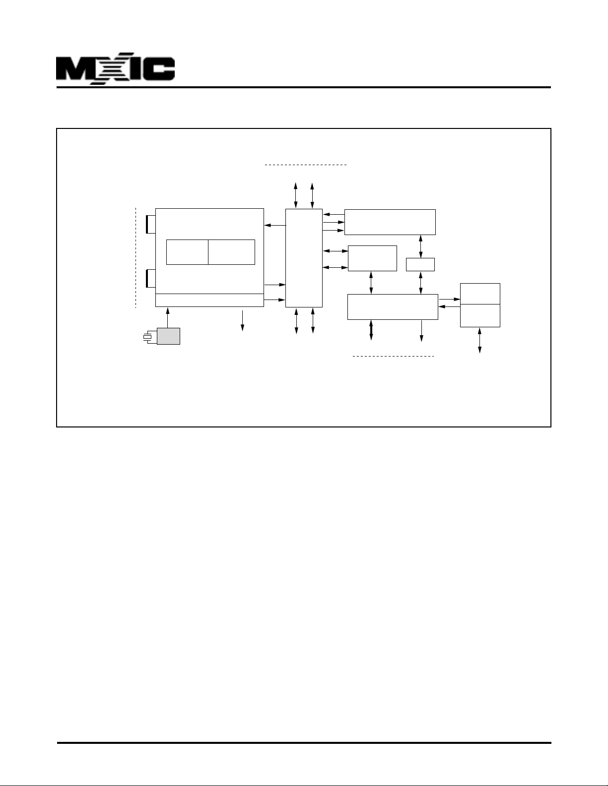
BLOCK DIAGRAM
S/T Interface
MX97102
Control and Data
Interface signals
PIDP0 PIDP1
7.68MHZ
Transmitter
Multiframe
control
Receiver
OSC
LAP-D
Activation/
Deactivation
DPLL
ECHO
GCI
Interface
PDCL PFSC1
B-channel
Switching
uP
Interface
microprocessor interface
FIGURE 2: FUNCTIONAL BLOCK DIAGRAM
FIFO
WATCH
DOG
RESET
SOURCE
PINTN
PRST
P/N:PM0473
REV. 2.5, SEP. 05, 2000
2
Page 3

MX97102
PIN DESCRIPTION (44-PIN)
TABLE 1: MX97102 PIN DESCRIPTIONS
LQFP PLCC
PAD# PAD# PIN NAME I/O DESCRIPTION
37 41 PAD0(D0) Multiplexed Bus Mode:Address/data b us from the CPU system to this devic
38 42 PAD1(D1) ,and data between the CPU system and this device.
39 43 PAD2(D2) Non-Multiplexed Bus Mode:Data bus between the CPU system and this
40 44 PAD3(D3) I/O device.
41 1 PAD4(D4)
42 2 PAD5(D5)
43 3 PAD6(D6)
44 4 PAD7(D7)
27 37 PCSN I ChipSelect:A logic "LOW" enable this device for a read/write operation.
28 38 PWRN(R/W) I Read/Write:A logic "HIGH" indicates a valid read operation by CPU.
A logic "LOW" indicates a valid write operation by CPU.(Motorola bus
mode) Write:A logic "LOW" indicates a write operation.(Intel bus mode)
29 39 PRDN(DS) I Data Strobe:
The rising edge marks the end of a valid read or write operation (Motorola
bus mode). Read:A logic "LOW" indicates a read operation.(Intel bus mode)
8 23 PINTN Open Interrupt Request:The signal is a logic "LOW" when this device
requests an Drain interrupt. It is an open drain output.
1~5, 14 NC
9,13,15 19,20 No used.
17~20 29,30
31~36
45~49
56,60
26 36 PALE I Address Latch Enable:A logic "HIGH" indicates an address on the address/
data bus(Multiplex ed b us type only). ALE also selects the micro-processor
interface type (multiplexed or non-multiplexed).
54 9 PRST I/O Reset:A logic "HIGH" on this input forces this device into reset state. The
minimum pulse length is four DCL-clock periods or four ms. If the terminal
specific functions are enabled,this device may also output a reset signal.
59 13 PFSC1 O(I) Frame Sync 1:Frame sync output. Logic "HIGH" during channel 0 on the
GCI interface. This pin becomes Input if Test Mode is programmed (register
ADF1).
58 12 PDCL O(I) Data Clock:Clock of frequency, 1536kHz output, equals to twice the GCI
data rate.
This pin becomes Input if Test Mode is programmed (register ADF1)
62 16 ECHO O This pin output the Echo bit from the receiving line.
P/N:PM0473
REV. 2.5, SEP. 05, 2000
3
Page 4

MX97102
TABLE 1: MX97102 PIN DESCRIPTIONS(Continued)
LQFP PLCC
PAD# PAD# PIN NAME I/O DESCRIPTION
(non-multiplex ed b us mode)
30 40 PA0 I Address Bit 0
51 6 PA1 I Address Bit 1
50 5 PA2 I Address Bit 2
64 18 PA3 I Address Bit 3
63 17 PA4 I Address Bit 4
55 10 PA5(EAW) I Address Bit 5; External Awake, when terminal specific function en
abled, this pin is used as an external awak e line. If a falling edge on this
input is detected, it generates an interrupt and a reset pulse.
7 22 PBCL O Bit Clock:Clock of frequency 768kHz equal to the GCI data rate.
52,53 7,8 PSDS1,2 O Serial Data Strobe 1&2 : programmable strobe signals , selecting either
one or two B or IC channels on GCI interface, is supplied via this line.
(registers ADF2,4)
6,57,61 11, 15
21 VSSD - Digital ground
10 24 VSSA - Analog ground
21 31 VDD - Power supply (5V±5%)
12 26 PXTAL1 I Connection for crystal or external clock input.
11 25 PXTAL2 O Connection for external crystal. Left unconnected if external clock is
used.
14 27 PSR2
16 28 PSR1 I S-Bus Receiver Input
22 32 PSX1 S-Bus Transmitter Output(positive)
23 33 PSX2 O S-Bus Tr ansmitter Output(negative)
24 34 PIDP0(DD) GCI-Data Port 0 (DD)
25 35 PIDP1(DU) I / O GCI-Data Port 1 (DU)
Open drain without internal pull-up resister or push-pull.
ABSOLUTE MAXIMUM RATINGS
TABLE 2: ABSOLUTE MAXIMUM RATINGS
RATING VALUE
Maximum Supply Voltage (VDD) 6V
DC Input Voltage on any pin -0.4Vto VDD+0.4V
Storage Temperature Range -55°C to 150°C
Operating Free Air Temperature Range 0°C to 70°C
P/N:PM0473
REV. 2.5, SEP. 05, 2000
4
Page 5

MX97102
DC CHARACTERISTICS
TABLE 3: DC CHARACTERISTICS
Temperature from 0 to 70°C; VDD = 5V±5%, VSSA = 0V, VSSD = 0V
Symbol Parameter Conditions Min. Value Max. V alue Unit Remarks
VIL L-input voltage -0.4 0.8 V
VIH H-input voltage 2.0 VDD+0.4 V All pins except
VOL L-output voltage IOL= 2mA 0.45 V PSX1, PSX2,
VOL1 L-output voltage (IDP0) IOL= 7mA 0.45 V PSR1, PSR2
VOH H-output voltage IOH= -400uA 2.4 V
VOH H-output voltage IOH= -100uA
VDD-0.75 V
ILI Input leakage current 0<VIN<VDD to 0V ±10 All pins except
BCL, PSX1,2,
ILO Output leakage current 0<VOUT<VDD to 0V ±10 uA PSR1,2, PA0,
PA1, PA3, PA4
ILIPD Input leakage current,
internal pull-down 0<VIN<VDD to 0V 120 uA PA0, PA1, PA3,
PA4, BCL
VX Absolute value of RL = 50ohm 2.03 2.31
output pulse amplitude RL = 400ohm 2.35 2.65 V PSX1, PSX2
(VSX2 - VSX1)
IX Transmitter out-
put current RL = 5.6ohm 7.5 13.4 mA
RX Transmitter out- Inactive or during
put impedance binary one 10 kohm
during binary zero 0 ohm
RL = 50ohm
VSR1 Receiver output voltage IO < 5uA 2.35 2.63 V PSR1, PSR2
VTR Receiver threshold Dependent on
voltage (VSR2 - VSR1) peak level 225 375 mV
P/N:PM0473
REV. 2.5, SEP. 05, 2000
5
Page 6
MX97102
AC CHARA CTERICS
TABLE 4: CRYSTAL SPECIFICATION
PARAMETER SYMBOL Limit values UNIT
Frequency f 7.680 MHz
Frequency calibration tolerance max. 100 ppm
Load capacitance CL max. 50 pF
Oscillator mode fundamental
XTAL1 Clock Characteristics (external oscillator
input)
TABLE 5: CLOCK CHARACTERISTICS
Parameter Limit values
min. max.
Duty cycle 1:2 2:1
Temperature from 0 to 70°C, VDD = 5V±5%
Inputs are driven to 2.4V for a logical "1" and to 0.4V
for a logical "0" . Timing measurements are made at
2.0V for a logical "1" and 0.8V f or a logical "0". The A Ctesting output is loaded with a 150pF capacitor.
TIMING WAVE FORM
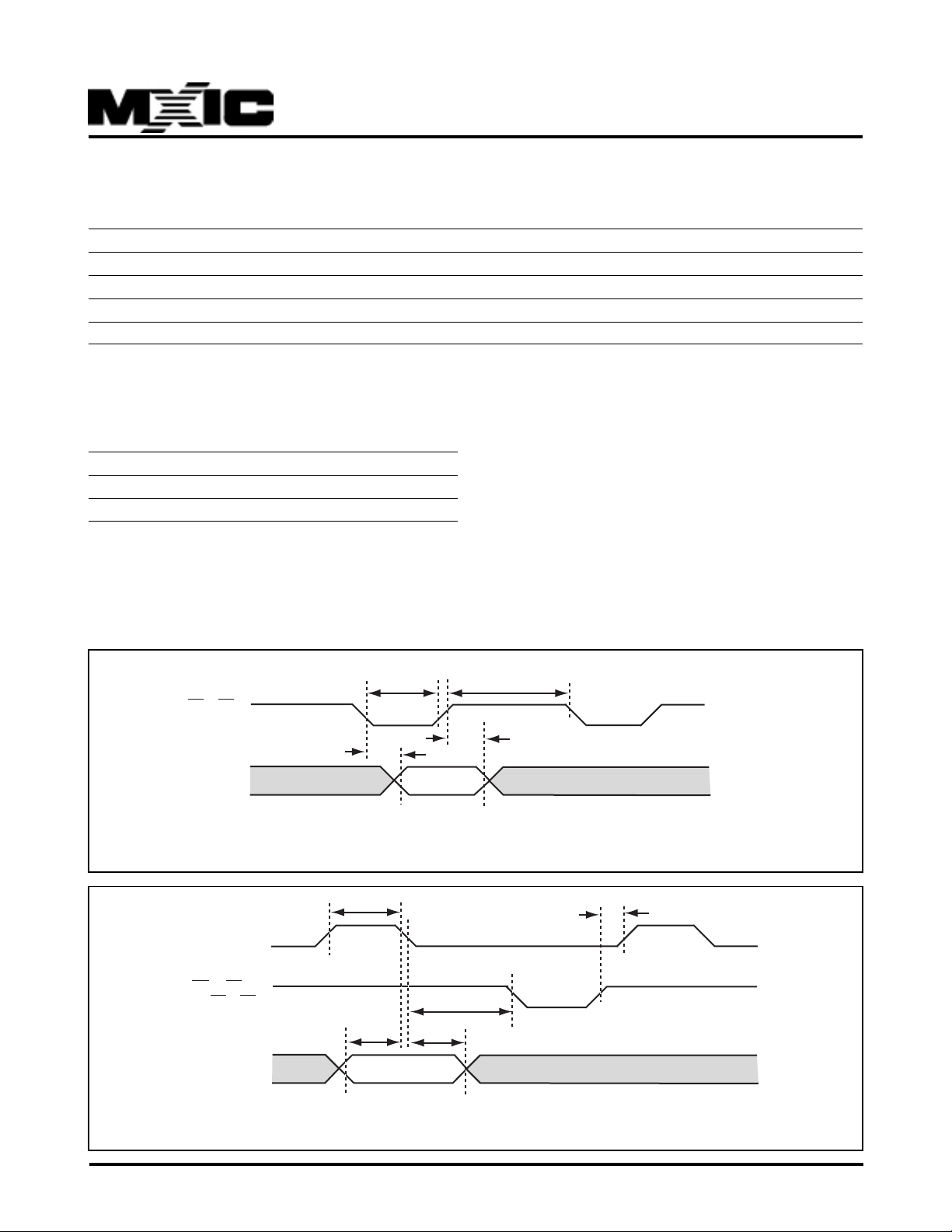
MICROPROCESSOR INTERFACE TIMING----INTERL BUS MODE
tRR
RD x CS
tRD
AD0-AD7
Data
FIGURE 3(a) MICROPRCESSOR READ CYCLE IN INTEL BUS MODE
tRI
tDF
P/N:PM0473
tAD
ALE
WR x CS or
RD x CS
AD0-AD7
tAA
tAL
tALS
tLA
Address
FIGURE 3(b) MICROPROCESSOR WRITE CYCLE IN INTEL BUS MODE
6
REV. 2.5, SEP. 05, 2000
Page 7
MX97102
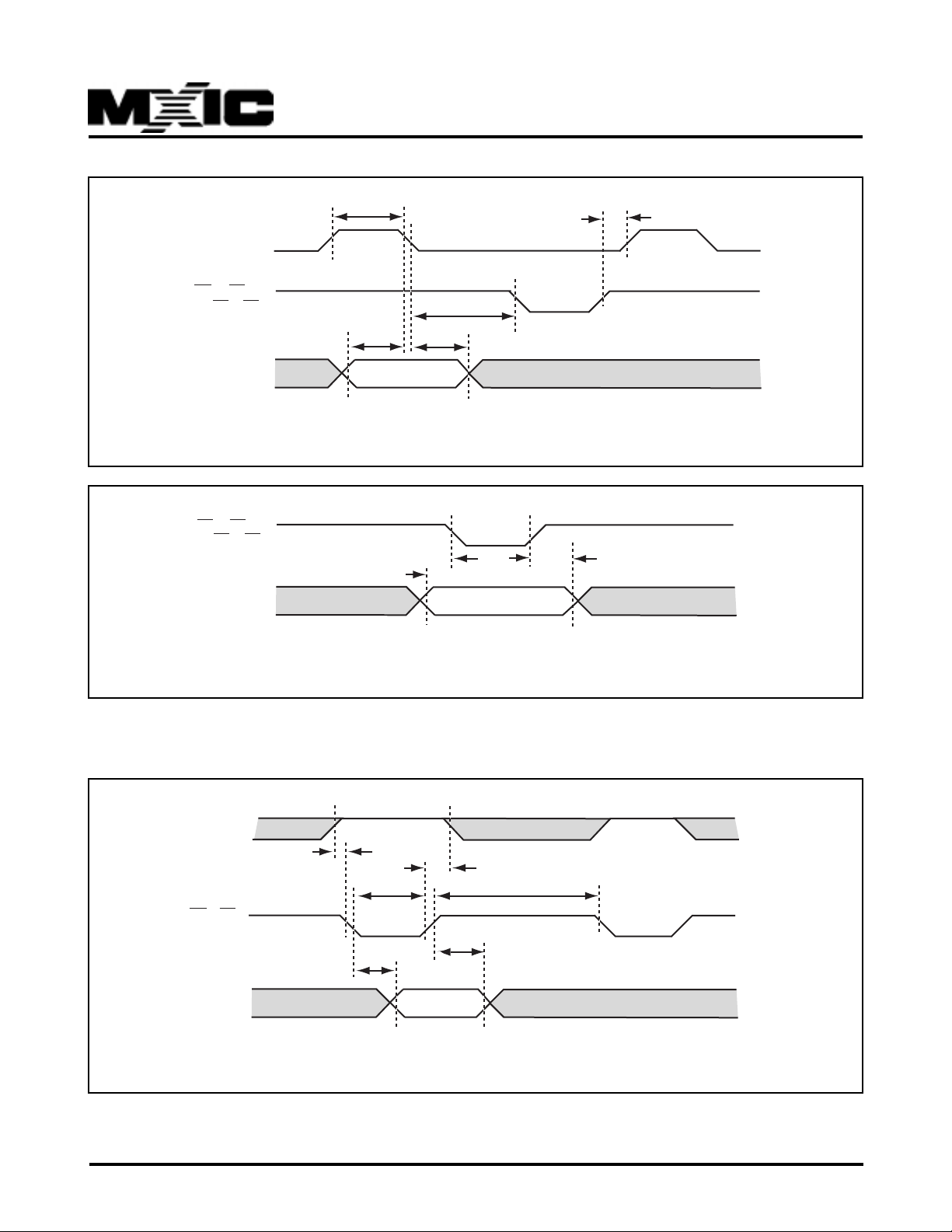
ALE
WR x CS or
RD x CS
AD0-AD7
FIGURE 3(c) MULTIPLEXED ADDRESS TIMING IN INTEL BUS MODE
WR x CS or
RD x CS
A0-A5
tAA
tAL
Address
tAS
tAD
tALS
tLA
tAH
Address
FIGURE 3(d) NON-MULTIPLEXED ADDRESS TIMING IN INTEL BUS MODE
MOTOROLA BUS MODE
ALE
CS x DS
D0-D7
FIGURE 4(a) MICROPROCESSOR READ TIMING IN MOTOROLA BUS MODE
tDSD
tRD
tRR
tRWD
tRI
tDF
Data
P/N:PM0473
REV. 2.5, SEP. 05, 2000
7
Page 8
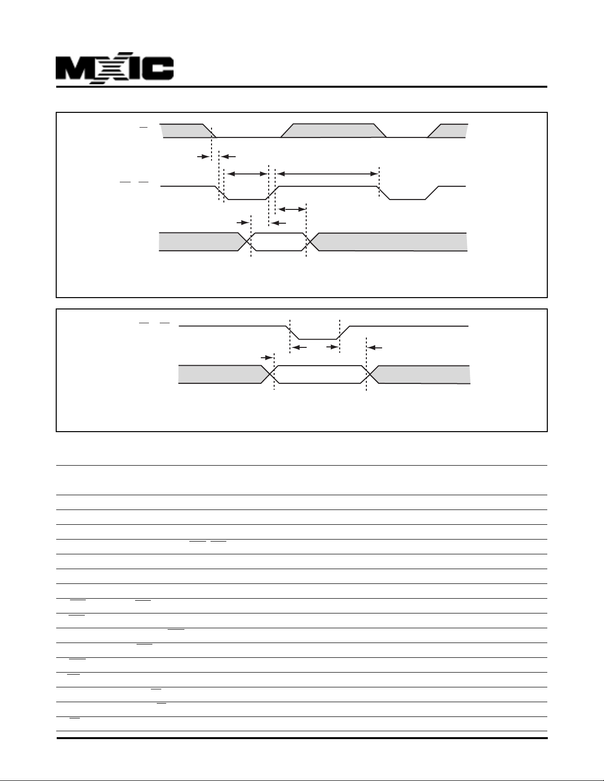
R/W
MX97102
tDSD
CS x DS
D0-D7
tWW
tWD
tDW
Data
tWI
FIGURE 4(b) MICROPROCESSOR WRITE TIMING IN MOTOROLA BUS MODE
CS x DS
AD0-AD5
tAS
Address
tAH
FIGURE 4(c) NON-MULTIPLEXED ADDRESS TIMING IN MOTOROLA BUS MODE
TABLE 6: PARAMETERS FOR MICROPROCESSOR INTERFACE TIMING
P ARAMETER SYMBOL Limit Value UNIT
min. max.
ALE pulse witdh tAA 40 ns
Address setup time to ALE tAL 10 ns
Address hold time to ALE tLA 10 ns
Address latch setup time to WR, RD tALS 0 ns
Address setup time tAS 10 ns
Address hold time tAH 10 ns
ALE guard time tAD 15 ns
DS delay after RW setup tDSD 0 ns
RD pulse width tRR 50 ns
Data ouput delay from RD tRD 50 ns
Data float from RD tDF 52 ns
RD control interval tRI 50 ns
W pulse width tWW 50 ns
Data setup time to W, CS tDW 10 ns
Data hold time from W, CS tWD 10 ns
W control interval tWI 50 ns
P/N:PM0473
8
REV. 2.5, SEP. 05, 2000
Page 9
Functional and Operational Description
ISDN ACCESS ARCHITECTURE
MX97102
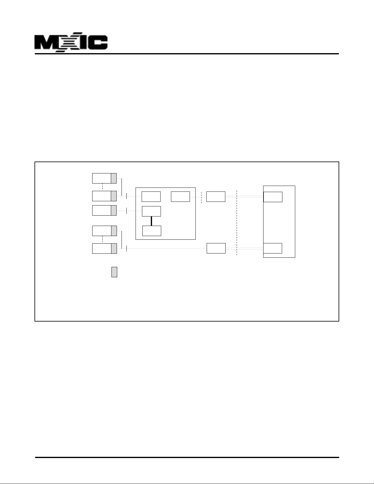
MX97102 is designed especially for subscriber terminal equipment with S/T interfaces, F our wire , tw o pairs
for transmission and receiption separately, are connected to the NT equipment at the user site. Via the NT
equipment, subscribers could dial up to the wide-area
network with the traditional telephone line. The NT
serves a converter between the U interface at the ex-
TE(1)
S
TE(8)
S
TE(1)
TE(1)
S
TE(8)
= MX97102
LT-S LT-T
LT-S
LT-S
Direct Subscriber Access
PBX(NT2)
where - TE is an ISDN terminal
- LT-S is a subscriber line termination
- LT-T is a trunk line termination
- LT is a trunk line termination in the central office
change and the S interface at the user premises. The
NT may be either an NT1 only or an NT1 together with
an NT2 connected via the T interface which is physically identical to the S interface. NT2 may include higher
level functions like multiplexing and switching as in a
PBX. Figure 5 illustrates the connections between the
user site to the public domain of central office.
ISDN
central office
T
NT1
U
telephone
line
LT
LTNT1
FIGURE 5 : ISDN - BASIC SUBSCRIBER ACCESS ACHITECTURE
MX97102 is based on the ISDN basic access, 192kbit/
s, which consists of two circuit-switched 64 kbit/s B
channels and a message oriented 16kbit/s D channel
for packetized data, signaling and telemetry information. The D channel is processed by the LAPD controller contained in the MX97102 and routed via a parallel
CPU interface to the terminal processor. The high level
support of the LAPD protocol which is implemented by
the MX97102 allows the use of a low cost processor in
cost sensitive applications.
P/N:PM0473
REV. 2.5, SEP. 05, 2000
9
Page 10
GCI CONNECTION
MX97102
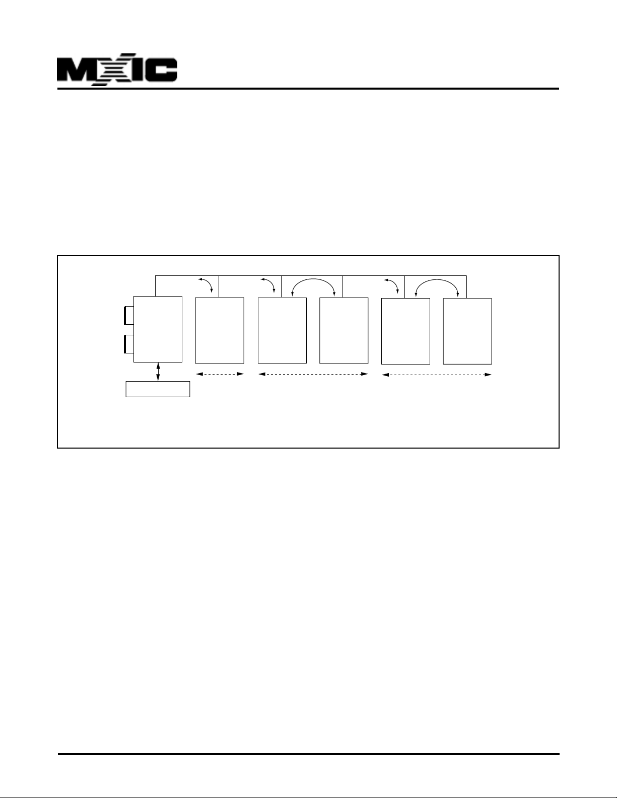
With the GCI interface, MX97102 could connect diff erent voice/data (V/D) application modules. Up to eight
D-channel components may be connected to the D and
C/I (Command/Indication) channels (TIC-bus). TIC-b us
arbitration is also implemented in MX97102.
Data transfers between the MX97102 and the V/D modules are done with the help of the GCI MONITOR channel protocol. Each V/D module can be accessed by an
MX97102
Microprocessor
D, C/I
Data
Module
A
Data
Module
B1
Speech
Processing
Speech Modules
FIGURE 6: EXAMPLES OF GCI CONNECTION
individual address. Two intercommunication channels
IC1 and IC2 allow a 2*64kbit/s transfer rate between
voice/data modules. Figure 6 shows one GCI connection, data module A uses D-channel for data transf er , a
voice processor is connected to a programmable digital processing codec filter via IC1 and a data encryption module to a data device via IC2. Meanwhile, B1 is
used for voice communication, B2 for data communication.
B1
DSP Codec
Module
Data
Encryption
Data Modules
Data
Module
B
GCI FUNCTIONS
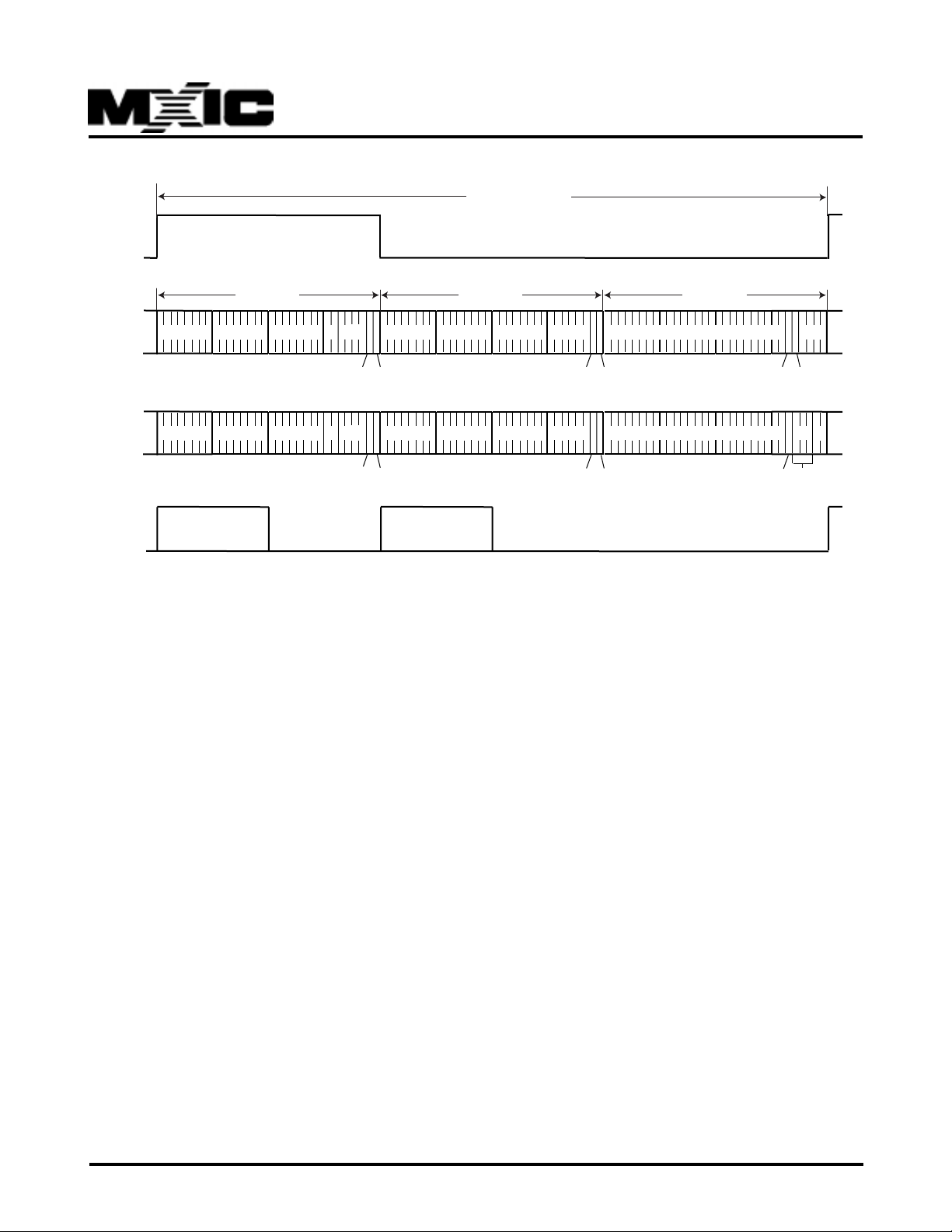
In terminal applications, the GCI constitutes a powerful backplane bus offering intercommunication and sophisticated control capabilities for peripheral modules. GCI frame is composed of three channels ( see Figure 6-1 belo w):
- Channel 0 contains 144kbit/s (for 2B+D) plus MONITOR and command/indication
channels for the layer-1 device.
- Channel 1 contains two 64kbit/s intercommunication channels plus MONITOR and
command/indication channels for other GCI devices.
- Channel 2 is used for GCI-bus arbitration. Only the command/indication are used in channel 2.
P/N:PM0473
10
REV. 2.5, SEP. 05, 2000
Page 11
FSC1
MX97102
125 us
CH0 CH1 CH2
IPD0
(DD)
IPD1
(DU)
SDS1
B1
B1
IDP0,1:768 kbit/s
DCL :1536 kHz
FSC1 :8 kHz
B2 MONO
B2 MONO D
CIO
D
MR MX
CIO
MR MX
IC1 IC2 MON1 CI1
IC1 IC2 MON1 CI1
BCL :768 kHz bit clock
SDS1 :8kHz programmable data strobe signal for
selecting one or both B/IC channel(s)
Figure 6-1 Frame structure of GCI
The GCI interface is operated in the “open drain” mode
in order to takes advantage of the b us capability. In this
case pull-up resisters (1kohm-5kohm) are required on
PIDP0 and PIDP1.
GCI OFF Function
In GCI terminal mode (SPCR:SPM=0) the GCI interface can be switched off f or external devices via IOF bit
in ADF1 register. If IOF=1, the interface is switched off .
Thus, DCL, FSC1, IDP0/1 and BCL are high impedence.
GCI Direction Control
MR MX S/G
MR MX
A/B
BAC TAD
GCI has the 12-byte frame structure consisting of channels 0, 1 and 2. (see figure 6-1 above)
- IDP0 carries the 2B+D channels from the S/T interface, and the MONITOR 0 and C/I 0 channels coming
from the S/T controller;
- IDP1 carries the MONITOR 0 and C/I 0 channels to
the layer-1.
Channel 1 of GCI interface is used f or internal communication in terminal applications. Two cases have to be
distinguished, according to whether the MX97102 is operated as a master device or as a slave device.
For test applications, the direction of IDP0 (DD) and
IDP1 (DU) can be reversed during certain time-slots
within the GCI frame. This is performed via the IDC bit
in the SQXR register. For normal operation SQXR:IDC
should be set to “0”.
P/N:PM0473
REV. 2.5, SEP. 05, 2000
11
Page 12
MX97102
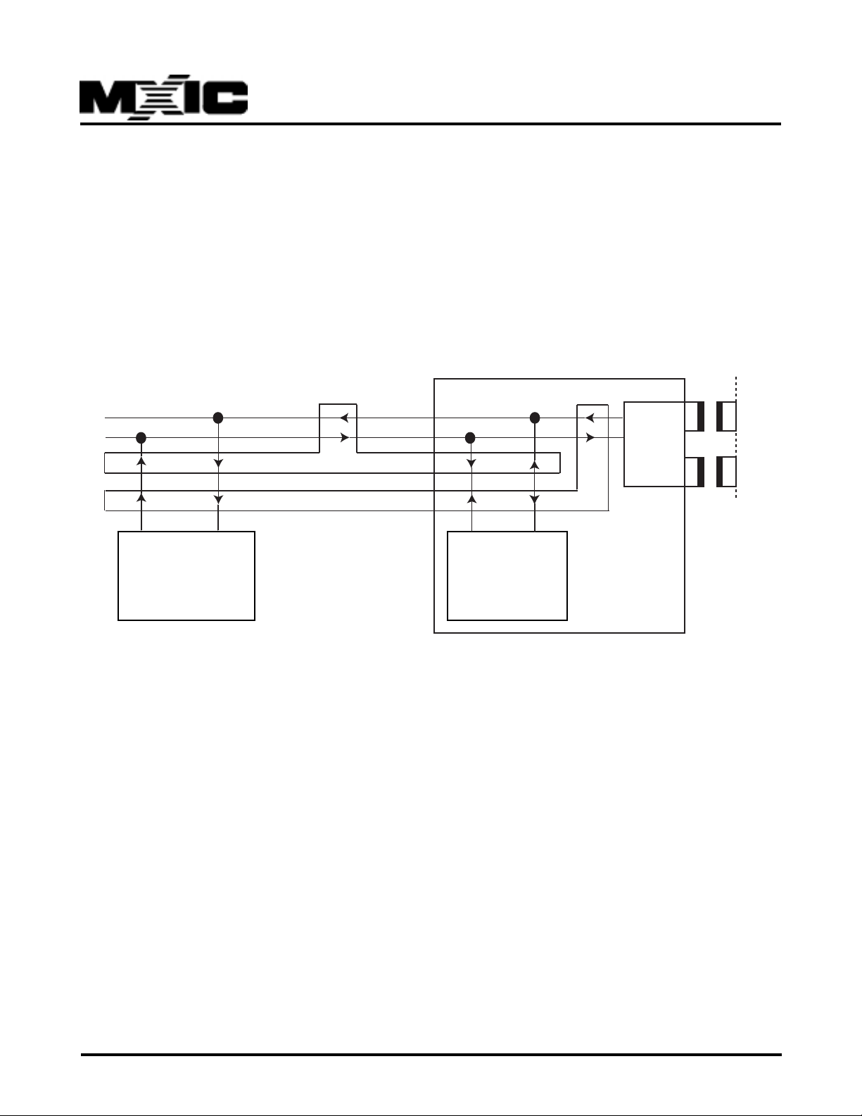
If IDC is set to "0" (master mode):
- IDP0 carries the MONITOR 1 and C/I 1 channels as output to peripheral (voice/data) devices;
- IDP0 also carries the IC channels as output to other devices, if programmed (CxC1-0=01 in register SPCR).
If IDC is set to "1" (slave mode):
- IDP1 carries the MONITOR 1 and C/I 1 channels as output to a master device;
- IDP0 carries the IC channels as output to other devices, if if programmed (CxC1-0=01 in register SPCR).
Figure 6-2shows the connection in a multifunctional terminal with the MX97102 as a master and a Voice/Data
module as a slave device.
S/T interface
GCI interface
DD
DU
IDP0
IDP1
IDP0
IDP1
IDP1
IDP0
MON1, C/I1, IC1, IC2
2B+D, C/I0, S/G, TIC
IDP1
IDP0
Layer1
MX97102
Voice/Data
Module as slave
Layer2
Figure 6-2 GCI port connection and Data direction
If GCI-0 of MODE register is programmed, bit 5 of the last byte in channel 2 on IDP0 can be used to indicate the
S-bus state (stop/go bit) and bit 2 to 5 of the last byte are used for TIC-bus access arbitration.
as Master
P/N:PM0473
REV. 2.5, SEP. 05, 2000
12
Page 13

Microprocessor Access to B and IC Channels
MX97102
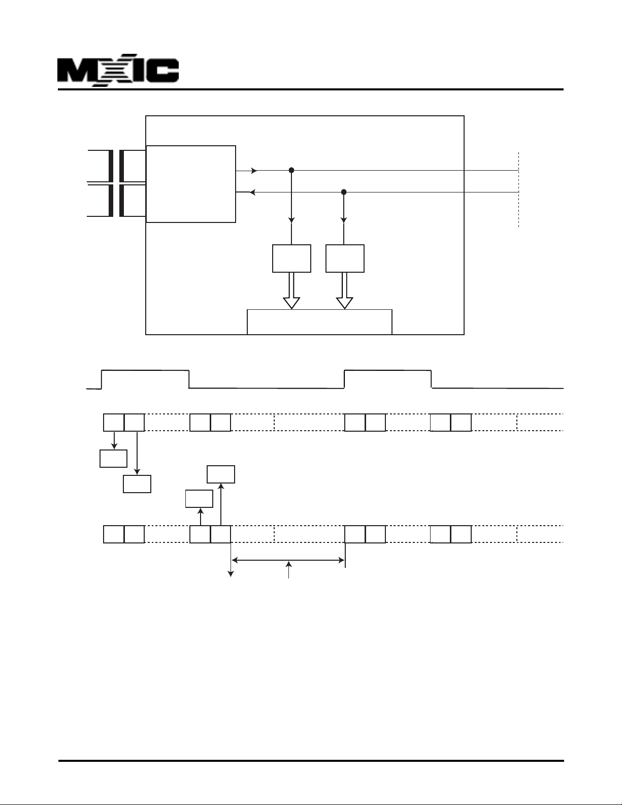
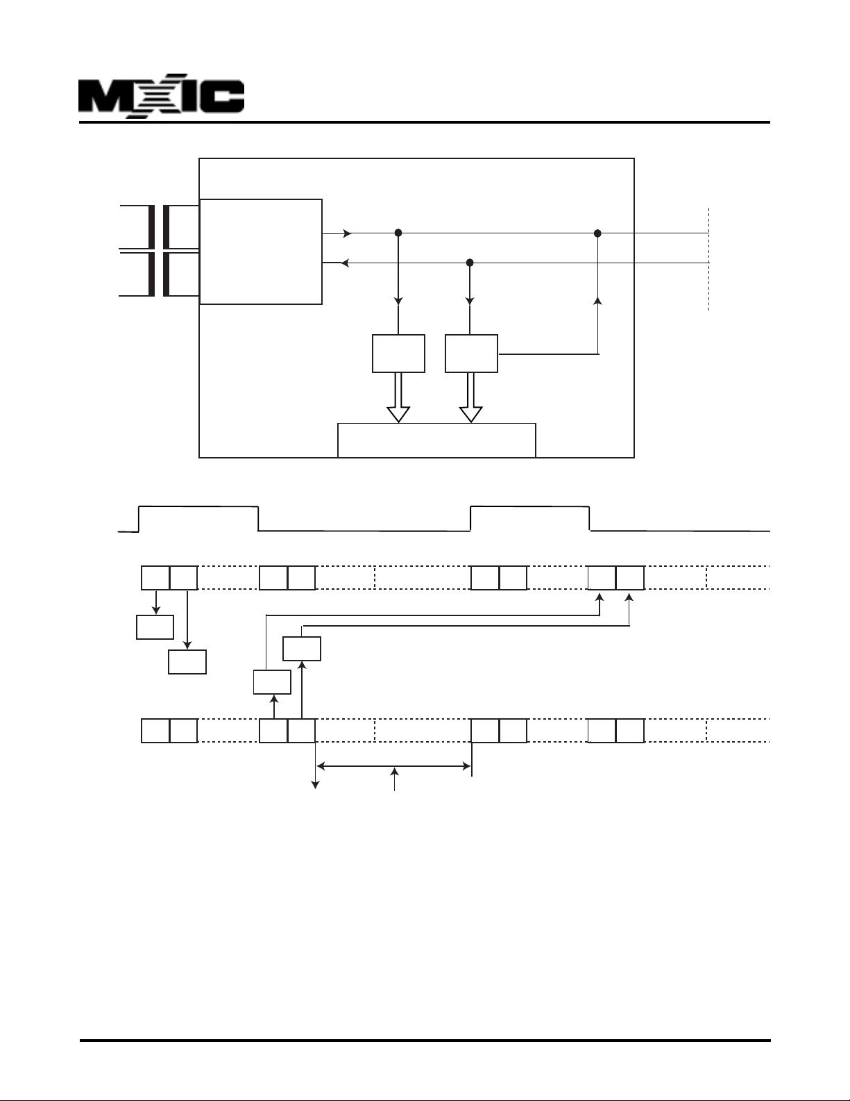
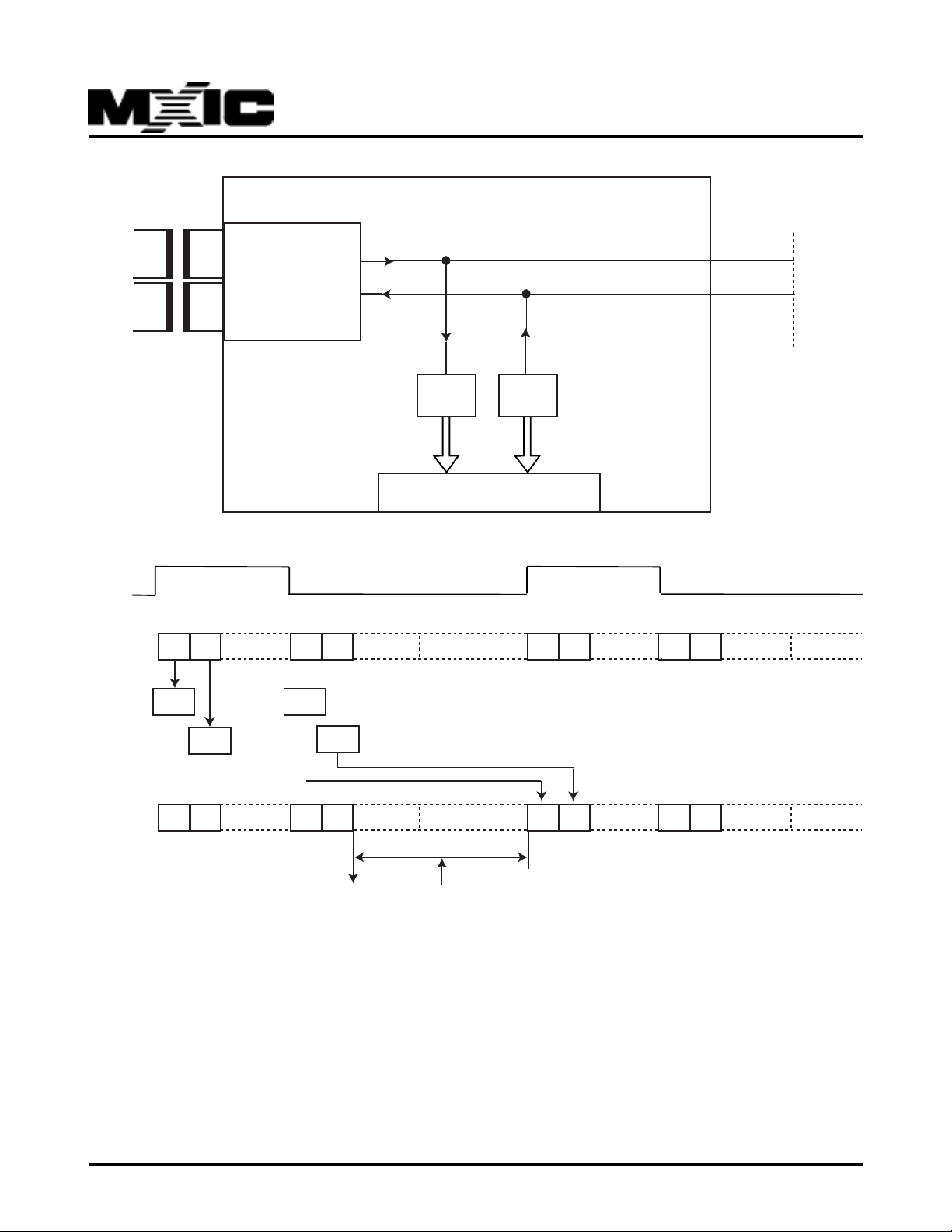
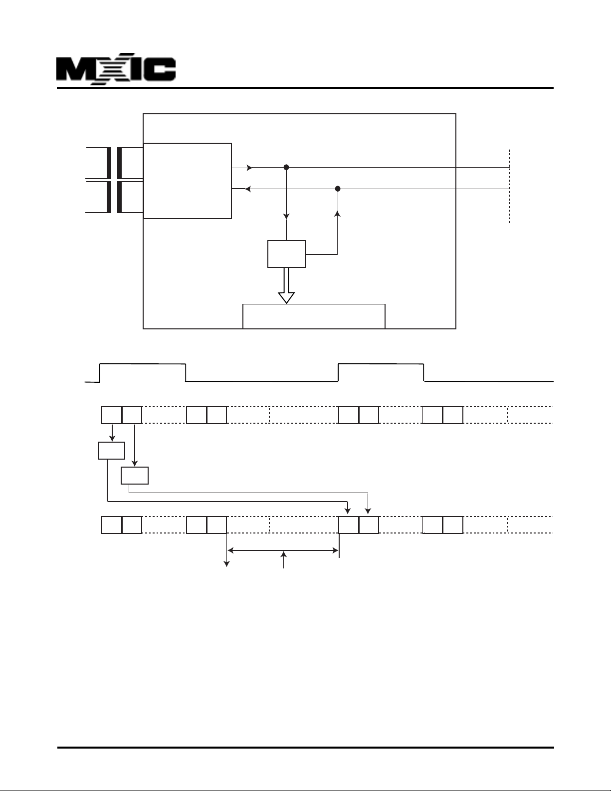
The microprocessor can access the B and IC channels
at the GCI interface by reading the B1CR/B2CR or by
reading and writing the C1R/C2R registers. Furthermore
it is possible to loop back the B channels from/to the S/
Four different functions are selected by the bits CxC1
and CxC0 in the SPCR register. Moreover, each channel, B channel 0/1 and IC channel 0/1, is programmed
individually. Table7-1 shows the configurations.
T interface or to loop back the IC channels from/to the
GCI interface without CPU intervention.
CxC1 CxC0 CxR Read CxR Write BxCR Read Output to GCI Applications
0 0 ICx - Bx - Bx, ICx monitoring
0 1 ICx ICx Bx ICx Bx monitoring, ICx looping
from/to GCI
1 0 - B x Bx Bx Bx access from/to S;
transmission of a constant
value in Bx channel to S
1 1 Bx Bx - Bx Bx looping from S;
transmission of a variable
pattern in Bx channels to S
Table 7-1 CPU access to B/IC channels by SPCR register
Note: x=1 for channel 1 or x=2 for channel 2
If the B-channel access is used for transferring 64kbit/
s voice/data information directly from the CPU port to
the ISDN S/T interface, the access can be synchronized to the GCI interface by means of a synchronous
transfer interrupt programmed in the STCR register.
The general sequence of operations to access the B/
IC channels is:
1. Program synchronous interrupt (ST0) which causes
the device to generate an SIN interrupt at the beginning of an GCI frame.
2. Read or write register (BxCR, CxR)
3. Set SC0 bit in the STCR to acknowledge SIN interrupt.
repeat this sequence from 1 to 3.
Same procedure could be used at ST1 and SC1 bits in
the STCR register. The only difference is ST1 gener-
ates an SIN interrupt at the middle of an GCI frame
instead of at the beginning.
When CPU accesses B channels, we can set the IOF
bit to switch off the GCI function. Thus , external B-chan-
nel sources (voice/data modules) can not disturb the
B-channel access on the GCI interface.
P/N:PM0473
REV. 2.5, SEP. 05, 2000
13
Page 14
MX97102
FSC
IDP0
(DD)
S/T Interface
B2 B1 B2 IC1 IC2IC1 IC2
B1
Layer-1
Functions
Bx ICx
BxCR
uP
GCI Interface
IDP0(DD)
IDP1(DU)
CxR
IDP1
(DU)
B1CR
B2CR
C1R
B1 B2 B1 B2 IC1 IC2IC1 IC2
Figure 6-3(a) SPCR : (CxC1, CxC0) = (0,0) Bx and ICx monitoring
C2R
ST0
SCO=1
P/N:PM0473
REV. 2.5, SEP. 05, 2000
14
Page 15
MX97102
FSC
IDP0
(DD)
S/T Interface
B2 B1 B2 IC1 IC2IC1 IC2
B1
Layer-1
Functions
Bx ICx
BxCR
uP
GCI Interface
IDP0(DD)
IDP1(DU)
CxR
IDP1
(DU)
B1CR
C1R
C2R
ST0
SCO=1
B2CR
B1 B2 B1 B2 IC1 IC2IC1 IC2
Figure 6-3(b) SPCR : (CxC1, CxC0) = (0,0) Bx and ICx monitoring, ICx looping (SQXR : IDC = 0)
P/N:PM0473
REV. 2.5, SEP. 05, 2000
15
Page 16
MX97102
FSC
IDP0
(DD)
S/T Interface
B2 B1 B2 IC1 IC2IC1 IC2
B1
Layer-1
Functions
Bx Bx
BxCR
uP
GCI Interface
IDP0(DD)
IDP1(DU)
CxR
IDP1
(DU)
B1CR C1R
B2CR
B1 B2 B1 B2 IC1 IC2IC1 IC2
Figure 6-3(c) SPCR : (CxC1, CxC0) = (1,0) Bx access from/to S/T
transmission of constant value of S/T
C2R
ST0
SCO=1
P/N:PM0473
REV. 2.5, SEP. 05, 2000
16
Page 17
MX97102
FSC
IDP0
(DD)
S/T Interface
B2 B1 B2 IC1 IC2IC1 IC2
B1
Layer-1
Functions
GCI Interface
IDP0(DD)
IDP1(DU)
Bx Bx
CxR
uP
IDP1
(DU)
B1CR
B2CR
B1 B2 B1 B2 IC1 IC2IC1 IC2
Figure 6-3(c) SPCR : (CxC1, CxC0) = (1,1) Bx looping from/to S/T
transmission of variable pattern of S/T
ST0
SCO=1
P/N:PM0473
REV. 2.5, SEP. 05, 2000
17
Page 18
MONITOR channel handling
MX97102
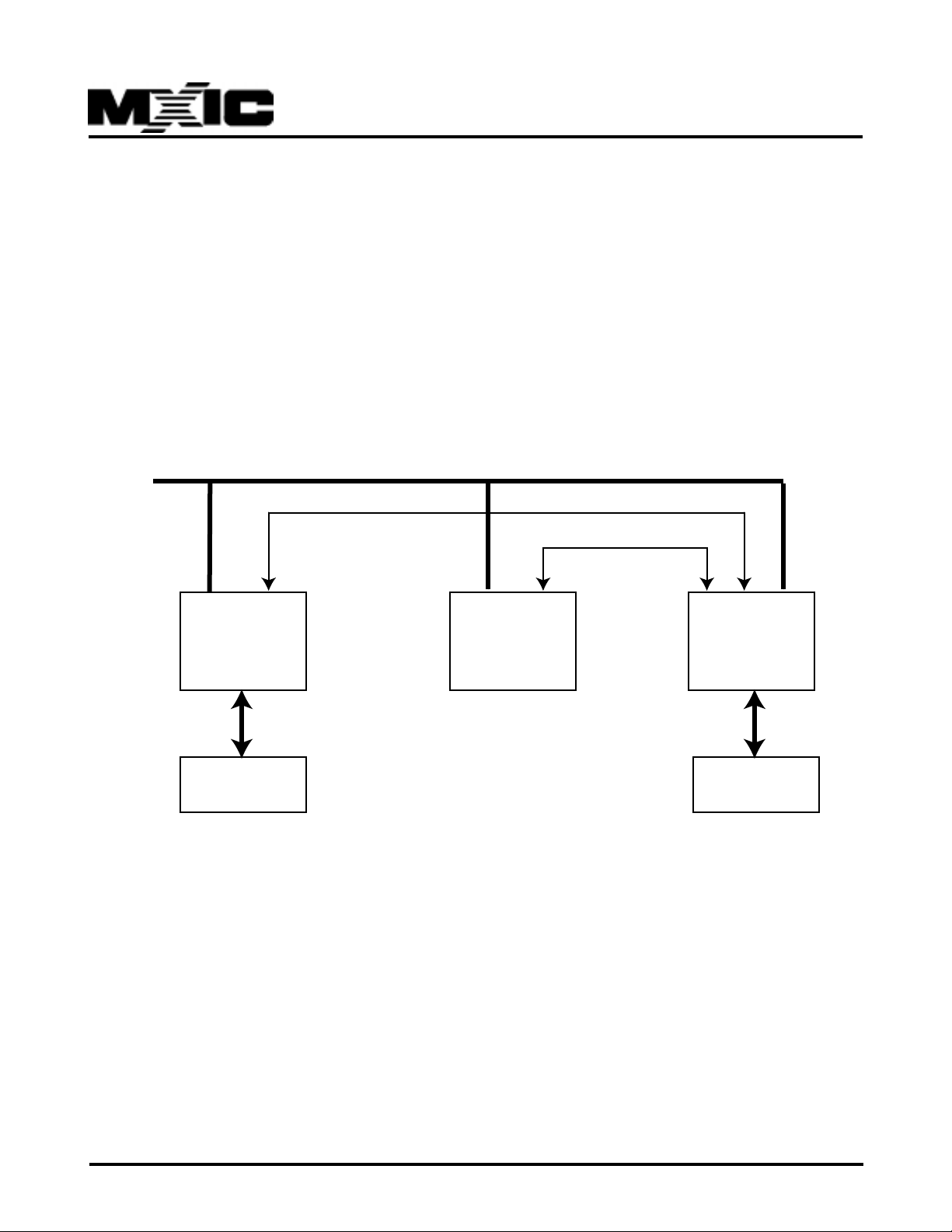
The MONITOR channel protocol is a handshake protocol used for high speed information exchange betw een
the MX97102 and other devices.
The usage of the MONITOR channel protocol (see Figure 6-4 below):
- For programming and controlling devices attached to
the GCI. Examples of such devices are layer-1 transceivers (using MONIT OR channel 0), and peripheral V/
D modules that do not need a parallel microcontroller
interface (by using MONITOR channel 1), such as the
Audio Ringing Codec Filter.
Data Communication
(MONITOR1)
V/D Module
- For data exchange between two microcontroller systems attached to two different devices on one GCI
backplane. Use of the MONITOR channel avoids the
necessity of a dedicated serial communication path between the two systems. This simplifies the system design of terminal equipments.
Note: MX97102 does not support the “MONITO R channel 0” operation. The implemented MONITOR handler
can howev er be used with external lay er-1 transceivers
in case only the ICC part of this device is used (ADF1:
TEM, PFS).
Control (MONITOR1)
V/D Module MX97102
CPU
CPU
Figure 6-4 MONITOR channel applications in GCI interface
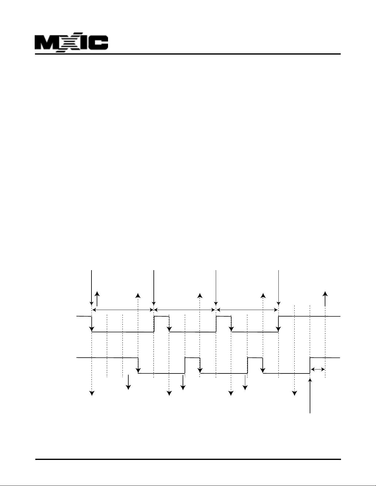
The MONITOR channel operates on an asynchronous basis. While data transfers on the bus take place synchronized to frame sync, the flow of data is controlled b y a handshake procedure using the MONIT OR Channel Receive
(MR0 or MR1) and MONITOR Channel Transmit (MX0 or MX1) bits. For example: data is placed onto the MONITOR channel and the MX bit is activated. The data will be transmitted repeatedly once per 8kHz frame until the
transfer is acknowledge via the MR bit.
P/N:PM0473
18
REV. 2.5, SEP. 05, 2000
Page 19
MX97102
The microprocessor may either enforce a "1" in MR,
MX by setting the control bit MRC1, MRC0 or MXC1,
MXC0 of the MOCR register to logic 0, or enable the
control of these bits internally by the MX97102 according to the MONITOR channel protocol. Thus, before a
data exchange can begin, the control bit MRC(1,0) or
MXC(1,0) should be set to "1" by the microprocessor.
MONITOR handshake procedure
- Idle
The MX and MR pair being held inactive for
two or more frames constitutes the channel being idle
in that direction.
- Start of transmission
Before starting a transmission, the CPU should
verify that the transmitter is inactive , i.e. that a possib le
previous transmission has been terminated. This is indicated by a "0" in the MONITOR Channel Activ e (MAC)
status bit. After having written the MONITOR Data
Transmit (MOX) register, the microprocessor sets the
MONITOR Transmit Control bit (MXC) to "1". This enables the MX bit to go active (0), indicating the pres-
ence of valid MONITOR data (contents of MOX) in the
corresponding frame and remains active until an inactive-to-active transition (MDA) of MR is received, indicating the receiver has read the data off the bus. As a
result, the receiving device stores the MONITOR byte
in its MONITOR Receive register (MOR) and generates an MDR interrupt status.
There are two different cases, general case and maximum speed case, of the MONITOR handshake protocol. Bit MAX0(1) in the ADF3 register is set to "1" for
selecting the maximum speed case of MONITOR 0(1).
* As a general case (MAX=0):
The next byte is placed on the bus after the
inactive to active transmission of MR as early as the
next frame ( there is no limit to the maxim um number of
frames). At the time that the second byte is transmitted, MX is returned inactive for one frame time (MX
inactive for more than one fr ame time indicates an end
of message). In response to MX going active, MR will
be deactivated for one frame time (the MX inactive to
MR inactive delay can be any number of frame times)
after MOR is read. This procedure is repeated f or each
additional byte. (see Figure6-5)
Transmitter
Receiver
MXE=1
MXC=1
MX
MR
MOX=1st
MAC=1
1st byte
RD MOR
MOX=2nd
MDA
2nd byte nth byte
RD MOR RD MOR
MOX=nth MXC=0
MDA MDA
Figure 6-5 Timing chart of general case
MAC=0
EOM
125us
MERMDRMDRMDR
MRC=0
P/N:PM0473
REV. 2.5, SEP. 05, 2000
19
Page 20
As a maximum speed case (MAX=1):
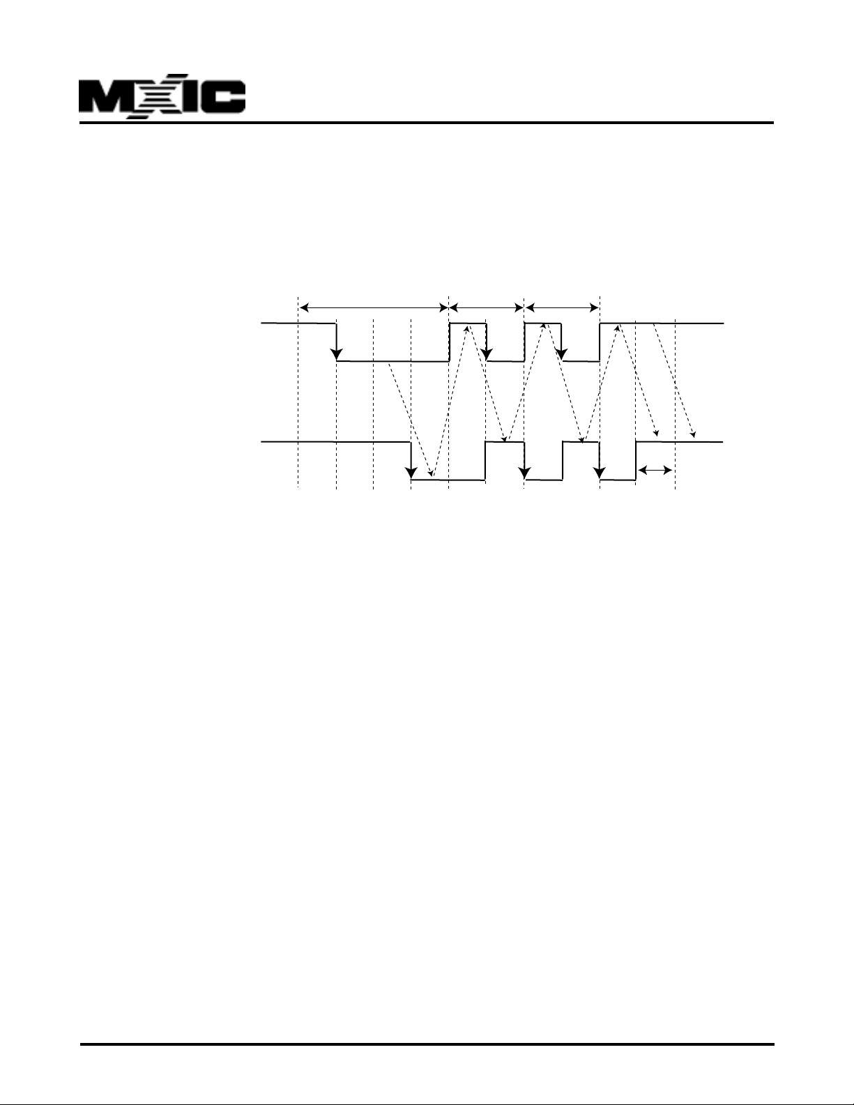
The transmitter can be designed for a higher
data throughput than is provided by the general case
described above. The transmitter can deactivate MX
and transmit new data one frame time after MR is deactivated. In this wa y , the transmitter is anticipating that
MX97102
MR will be reactivated one frame time after it is deactivated, minimizing the delay betw een bytes (see Figure
6-6). Note that MR being held inactive for two or more
frame times indicates an abort is being signaled by the
receiver .
1st byte
Transmitter
MX
MR
Receiver
* Transmitter anticipates the falling edge of the receiver's acknowledgment
*Signals from/to CPU are the same with general case(Figure6-8)
Figure 6-6 Timing chart of maximum speed case
- First byte reception
At the time the receiver sees the the first byte,
indicated by the inactive-to-active transition of MX
(MDR), MR is by definition inactive. In response to the
activation of MX, microprocessor reads the MONIT OR
Receive (MOR) register . When it is ready to accept data
(e.g. based on the value in MOR, which in a point-tomultipoint application might be the address of the
destinating device), it sets the MR contol bit (MRC) to
"1" to enable the receiver to store succeeding MONITOR channel bytes and acknowledge them according
to the MONITOR channel protocol. In addition, it enables other MONITOR channel interrupts by setting
MONITOR Interrupt Enable (MRE) to "1".
- Subsequent reception
Data is received from the bus on each falling
edge of MX, and a MDR is generated. Note that the
data may actually be valid at the time that MX went
inactive, one frame time prior to going active. MR is
deactivated after the data is read and reactivated one
frame time later. The transmitter will detect MR going
inactive and anticipate its reactivation one frame time
later. The transmission of the next data byte will begin
at the same time that MR is going active.
P/N:PM0473
2nd byte nth byte
EOM
125us
This "MDA interrupt - write data - MDR interrupt - read data - MDA interrupt" handshake is repeated
as long as the transmitter has data to send.
-End of transmission (EOM)
When the last byte has been acknowledged b y
the receiver, the microprocessor sets the MONITOR
Transmit Control bit (MXC) to "0". This enforces an inactive "1" state in the MX bit. Two frames of MX inactive signifies the end of a message. Thus, a MONITOR
Channel End of Receiption (MER) interrupt status is
generated by the receiver when the MX bit is received
in the inactive state in two consecutive frames. As a
result, the microprocessor sets the MRC to 0, which in
turn enforces an inactive state in the MR bit. This marks
the end of the transmission, making the MONITOR
Channel Active (MAC) bit return to “0”.
- Abort
During a transmission process, it is possible
for the receiver to ask a transmission to be aborted by
sending an inactive MR bit value in two consecutive
frames. This is effected by the microprocessor writing
the MRC bit to "0". An aborted transmission is indicated by a MONITOR Channel Data Abor t (MAB) interrupt status at the transmitter.
REV. 2.5, SEP. 05, 2000
20
Page 21

C/I-Channel Handling & TIC-Bus Access
MX97102
The command/indication channel carries real-time status information between the MX97102 and another device connected to the GCI.
- One C/I channel (called C/I 0) conve ys the commands
and indications between the layer-1 and the la yer-2 parts
of the MX97102. It can be accessed by an external
layer-2 device e.g. to control the layer-1 activation/deactivation procedures. C/I 0 channel access may be
arbitrated via the TIC b us access protocol. In this case
the arbitration is done in C/I channel 2.
The C/I 0 code is four bits long, could be read from
CIR0 (layer-1 to layer-2) and write to CIX0 (layer-2 to
layer-1).
In the receive direction, the code from layer-1 is continuously monitored, with an interrupt being generated
any time a change occurs (CISQ). A new code must be
found in two consecutiv e GCI fr ames to be considered
valid and to trigger a C/I code change interrupt status
(double last look criterion).
- A second C/I channel (called C/I 1) can be used to
convey real time status information between the
MX97102 and various non-layer-1 peripheral devices
such as ARCOFI. The channel consists of six bits in
each direction.
The C/I 1 channel is accessed via registers CIR1 and
CIX1. A change in the received C/I 1 code is indicated
by an interrupt status without double last look criterion.
The TIC-b us arbitration mechanism implemented in the
last octet of GCI channel 2 of the GCI allows the access of external communication controller (up to 7) to
the layer-1 functions provided in the MX97102 and to
the D channel. To this effect the outputs of the controllers are wired-and connected to pin IDP1. The inputs of
the ICCs are connected to pin IDP0. External pull-up
resistors on IDP0/1 are required. The arbitration mechanism must be activated by setting MODE: DIM2-0=001.
An access request to the TIC b us ma y either be generated by software (CPU access to the C/I channel) or by
the MX97102 itself (transmission of an HDLC frame).
A software access request to the bus is effected by
setting the BAC bit (CIX0 register) to “1”.
In the case of an access request, the MX97102 checks
the Bus Accessed-bit (bit 5 of IDP1 last octet of CH2,
see Figure6-1) for the status “bus free”, which is indicated by a logical “1”. If the bus is free, the MX97102
transmits its individual TIC-bus address programmed
in the STCR register. The TIC bus is occupied by the
device which sends is address error-free. If more than
one device attempt to seize the bus simultaneously,
the one with the lowest address value wins.
When the TIC b us is seized by the MX97102, the BA Cbit on IDP1 is “0” until the access request is withdrawn.
After a successful bus access, the MX97102 is automatically set into lower priority class, that is, a new bus
access cannot be performed until the status “bus free”
is indicated in two successive frames.
If none of the devices connected to the GCI interface
request access to the D and C/I channels, the TIC-bus
address 7 will be present. The de vice with this address
will therefore have access, by default, to the D and C/I
channels. The availability of the S/T interface D channel is indicated in bit5 “Stop/Go” (S/G=1: stop, S/G=0:
go) of the IDP0 last octet of C/I channel (Figure6-1).
P/N:PM0473
REV. 2.5, SEP. 05, 2000
21
Page 22
MX97102
,
y
S/T interface
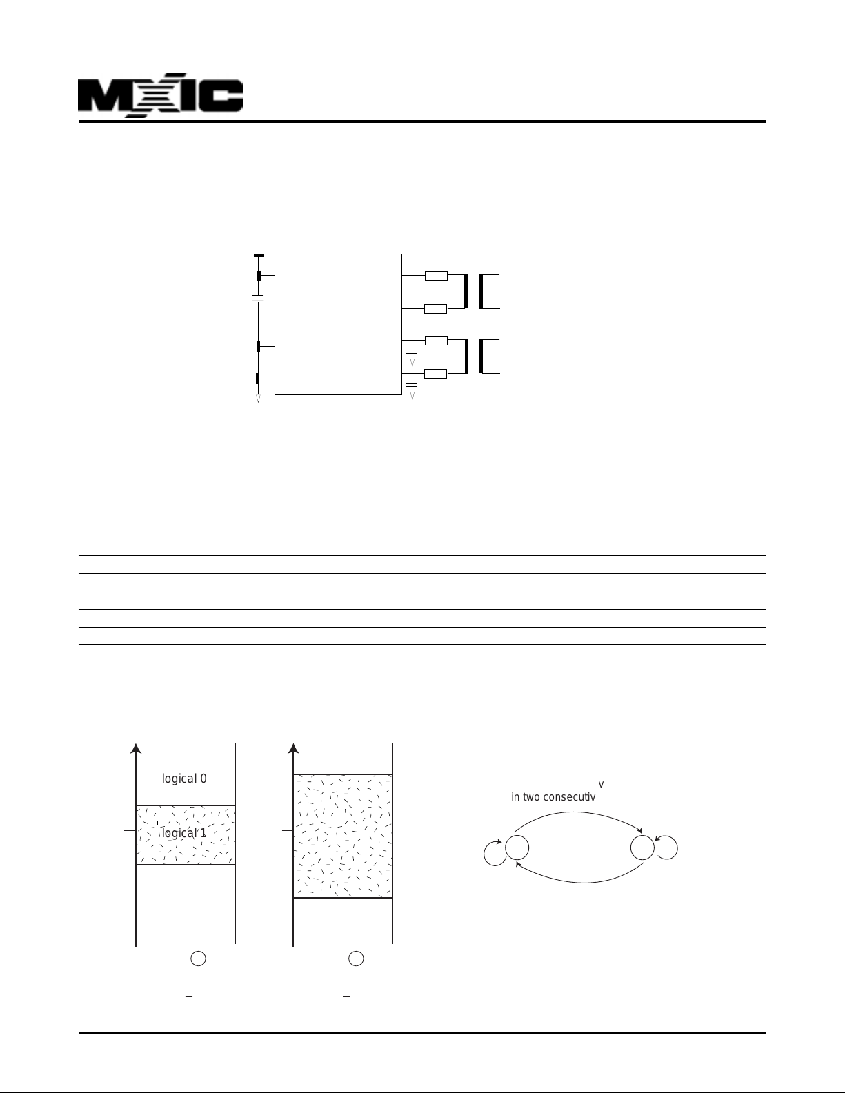
Line transceiver functions for the S/Y interface follow the electrical specifications of CCITT I.430. According to this
standard, pseudo-ternary encoding with 100% pulse width is used on the S/T interface. For both receive and
transmit direction, a 2:1 transformer is used to connect the MX97102 transceiver to the 4 wire S/T interface.
+5V
2 : 1
Transmit Pair
2 : 1
Receive Pair
Protection Circuits
10uf
GND
VDD
VSSD
VSSA
PSX1
PSX2
MX97102
PSR1
PSR2
FIGURE 6-7: MX97102 EXTERNAL S-INTERFACE CIRCUITRY
- Pre-Filter Compensation
To compensate for the extra delay introduced into the received signal by a filter, the sampling of the receive
signal can be delayed by programming bits TEM and PFS in the ADF1 register as shown below.
TEM PFS
0 0 no delay
0 1 delay 650ns
1 1 advance 390ns
1 0 test mode
The receiver is designed as a threshold detector with adaptively switched threshold levels. Pin PSR1 delivers 2.5V
as an output, which is the virtual ground of the input signal on pin PSR2. The detector controls the switching of the
receiver between two sensitivity levels (see Figure6-8).
+225mv
P/N:PM0473
V
SR2-VSR1
0v
-225mv
|
with Vtr1=+225mV
logical 0
logical 1
logical 0
state 1
High sensitivity
V
SR2-VSR1
+375mv
|Vmax| > 1v
in two consecutive frames
0v
1
750mv<|Vmax|<1v
-375mv
{
Vmax<750mv or
Vmax>750mv
state 2
Low sensitivity
with Vtr2=+375mV
Vtr1, Vtr2:threshold voltages of the receiver threshold detector
Vmax:maximum value of VSR2-VSR1 during one frame
Figure 6-8 State diagram of the adaptive receiver
22
2
750mv<|Vmax|<1v
REV. 2.5, SEP. 05, 2000
Page 23
MX97102
Activation/Deactivation
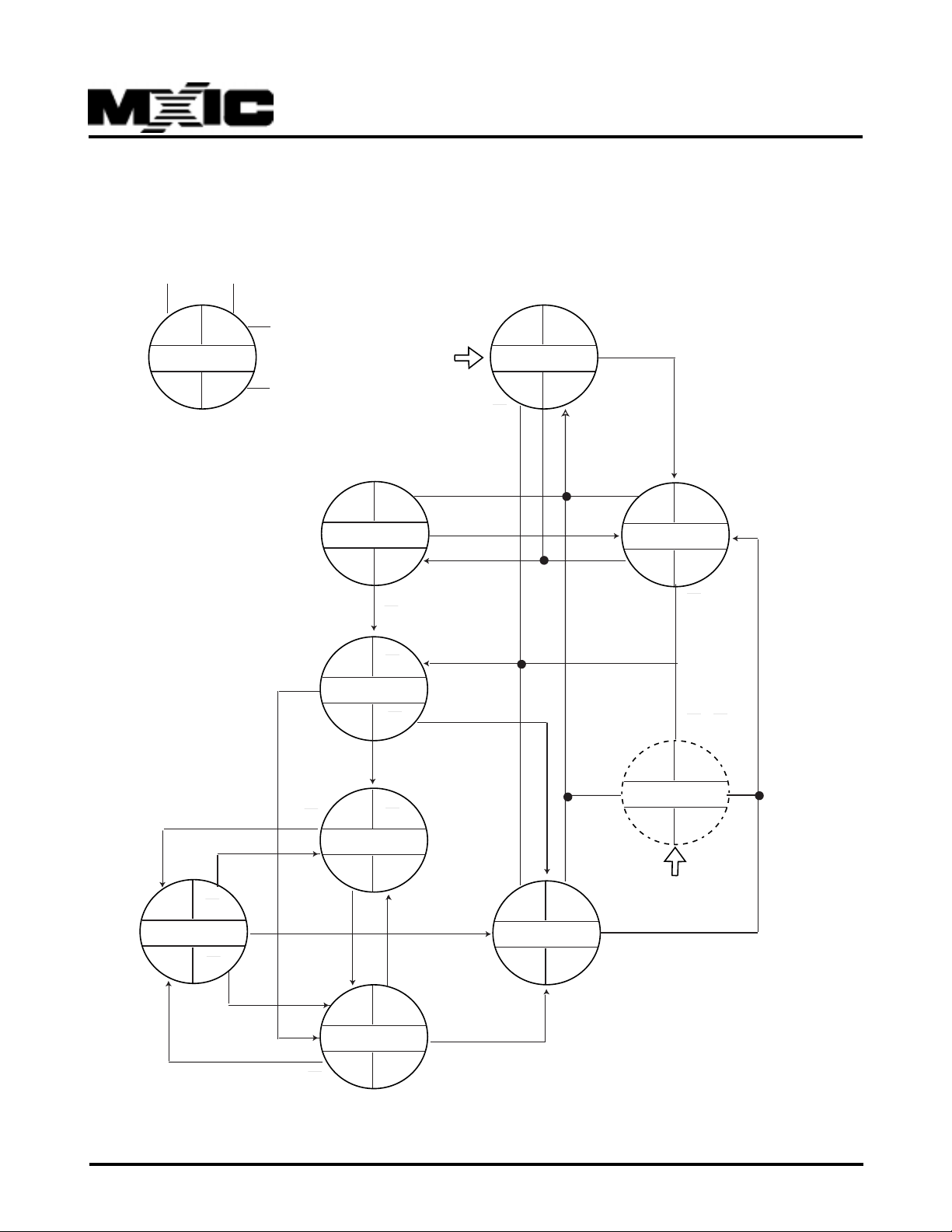
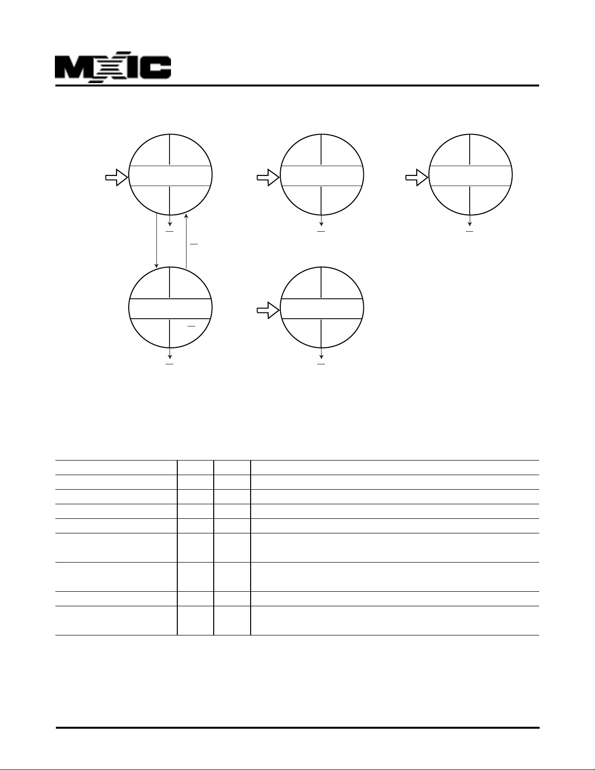
An incorporated finite state machine controls ISDN layer-1 activation/deactivation according to CCITT I.430. Figure6-9 shows the state diagrams. Table7-2 and Table7-3 indicate the command and indication code descriptions.
OUT IN
Ind.
iX
State
Cmd.
iR
IOM2
i4
DID
DIU
RST
S
DIU
PU
F4 Pend. Act.
RSYD
F5 Unsynchron.
ARD
i0
F6 Synchron.
ARU
i0
i1
i0
X
i0
i0
i2
X
TIM
i0
F3 Power Down
i0
i0
ARU
i0
ARU
i0.DIU
TIM
DIU
PU
F3 Power Up
i0
Uncond. States
TIM
i0
i0
i0
X
X
,
TIM
P/N:PM0473
RSYD
F8 Lost frame
X
i0
i0
i3
i2
i4
i0
i4
AID ARU
i0
i2
F7 Activated
i3
i4
DIU
DR ARU
F3 Pend. Deact.
i0
i2
i0
TIM
i0
X
X : unconditional command (ARL, RS, SSZ, SCZ)
Figure 6-9(a) State diagram
REV. 2.5, SEP. 05, 2000
23
Page 24
MX97102
ARL
PU
Loop 3 closed
i3 i3
TI
ATI
Loop 3 Act.
ARL
i3
i3
*
X
ARL
i0
i0/
X
Figure 6-9(b) State diagram : unconditional transitions
SCZ
SSZ
TI
Continuous Pulse
TIS
Single Pulse
SCZ
Test Mode
ic
X
SSZ
Test Mode
is
X
*
*
RS
is:Single pulse, 4kHz
ic:Test pulse, 96kHz
X:Forcing commands
EI
Reset State
i0
RS
X
*
Command (upstream) Abbr. Code Reamrks
Timing TI M 0000 Activation of all output clocks is requested
Reset RS 0001 ( X)
Send continuous zeros SCZ 0100 Transmission of pseudo-ternary pulses at 96kHz frequency (X)
Send single zeros S SZ 0010 Transmission of pseudo-ternary pulses at 2kHz (X)
Activate request AR8 1000 Activation command, set D-channel priority to 8
set priority 8
Activate request AR10 1001 Activation command, set D-channel priority to 10
set priority 10
Activate request loop ARL 1010 Activation of test loop 3 (X)
Deactivate indication DIU 1111 GCI-interface clocks can be disabled
upstream
Table 7-2 C/I command code descriptions
P/N:PM0473
24
REV. 2.5, SEP. 05, 2000
Page 25

MX97102
Note: When in the activated state (AI8/AI10) the 2B+D channels are only transferred from the GCI to the S/T
interface if an “Activate Request” command is written to the CIX0 register.
Indication Abbr. Code Reamrks
Power up PU 0111 GCI clocking is provided
Deactivate request DR 0000 Deactivation request by S interface
Error indication EI 0110 Either : (pin PRST = 1 and bit CFS = 0) or RS
Level detected RSYD 0100 Signal received, receiver not synchronous
Activate request ARD 1000 Info 2 received
downstream
Test indication TI 1010 Test loop 3 activated or continuous zeros transmitted
Awake test indication ATI 1011 Level detected during test loop
Activate indication AI8 1100 Info 4 received, D-channel priority is 8 or 9
with priority class 8
Activate indication AII0 1101 Info 4 received, D-channel priority is 10 or 11
Deactivate indication D ID 1111 Clocks will be disabled in MX97102, quiescent state
downstream
Single zero transmitted TIS 0101 Send single zeros at 2kHz frequency
Table 7-3 C/I command code descriptions
Level Detection Power Down
In power down state, only an analog le vel detector is activ e. All cloc ks, including the GCI interface, are stopped. The
data lines are "high" whereas the clocks are "low".
An activation initiated from the exchange side (Info2 in S bus detected) will have the consequence that a clock
signal is provided automatically.
From the terminal side an activation must be started by setting and resetting the SPU bit in the SPCR register.
P/N:PM0473
REV. 2.5, SEP. 05, 2000
25
Page 26

D-channel Access
MX97102
The D-channel access procedure according to CCITT
I.430 including priority management is fully implemented
in the MX97102. By programmed the DIM2-0 (MODE
register) to 001 or 011, stop/go bit is evaluated for Dchannel access handling, that is, a collision is detected
if the corresponding echo-bit value is different from the
transmitted D-bit value. When this occurs, D-channel
transmission is immediately stopped, and the echo
channel is monitored to enable a subsequent D-channel access to be attempted.
The priority class (prior ity 8 or priority 10) is selected
by transferring the appropriate activation command via
the command/indication (C/I) channel of the GCI interface to the layer-1 controller.
6.3.10 S- and Q- channel access
Access to the received/transmitted S- or Q- channel is
provided via registers. As specified by CCITT I.430,
the Q bit is transmited from TE to NT in the position
normally occupied by the auxiliary framing bit (FA) in
one frame out of 5, whereas the S bit is transmitted
from NT to TE in a spare bit (S). The functions provided
by the MX97102 are:
- When synchronism is achieved, the four received S
bits in frames 1, 6, 11, 16 are stored as SQR1 to SQR4
in the SQRR register if the complete M bit multiframe
pattern was correctly received in the corresponding
multiframe. A change in any of the received four bits is
indicated by an interrupt (CISQ in ISTA and SQC in
CIR0).
- When an M bit is observed to have a value different
from that expected, the synchronism is considered lost.
The SQR bits are not updated until synchronism is regained. The synchronization state is constantly indicated
by the SYN bit in the SQRR register.
- When synchronism with the received multiframe is
achieved, the four bits SQX1 to SQX4 stored in the
SQXR register are transmitted ad the four Q bit (FA-bit
position) in frames 1, 6, 11, 16 respectively (starting
from frame number one). Otherwise the bit tr ansmitted
a mirror of the received FA-bit. At loss of synchronism
(mismatch in M bit) the mirroring is resumed starting
with the next FA-bit.
- The S/T m ultiframe synchronization can be disabled in the STAR register (MULT bit).
- Synchronization to the received 20 frame multiframe
by means of the received M bit pattern. Synchronism is
achieved when the M bit has been correctly received
during 20 consecutive frames starting from frame number 1 (Table7-4).
P/N:PM0473
REV. 2.5, SEP. 05, 2000
26
Page 27

MX97102
Frame Number NT-to-TE FA-Bit position NT-to-TE M Bit NT-to-TE S Bit TE-to-NT FA-Bit position
1 ONE ONE S1 Q1
2 ZERO ZERO ZERO ZERO
3 ZERO ZERO ZERO ZERO
4 ZERO ZERO ZERO ZERO
5 ZERO ZERO ZERO ZERO
6 ONE ZERO S2 Q1
7 ZERO ZERO ZERO ZERO
8 ZERO ZERO ZERO ZERO
9 ZERO ZERO ZERO ZERO
10 ZERO ZERO ZERO ZERO
11 ONE ZERO S3 Q3
12 ZERO ZERO ZERO ZERO
13 ZERO ZERO ZERO ZERO
14 ZERO ZERO ZERO ZERO
15 ZERO ZERO ZERO ZERO
16 ONE ZERO S4 Q4
17 ZERO ZERO ZERO ZERO
18 ZERO ZERO ZERO ZERO
19 ZERO ZERO ZERO ZERO
20 ZERO ZERO ZERO ZERO
1 ONE ONE S1 Q1
2 ZERO ZERO ZERO ZERO
etc.
Table 7-4 S- and Q-channel Structure
Terminal Specific Functions
The MX97102 provides the follo wing optional functions
by setting bit TSF (STCR register) to “1”. When terminal specific functions are activated (TSF=1), bit RSS
(CIX0 register) is programmed for selecting Watchdog
Function (RSS=1) or External Awake Function (RSS=0).
Deactivating the terminal specific functions is only possible with a hardware reset.
Watchdog Function (TSF=1, RSS=1):
During every time period of 128ms the processor has
to program the WTC1 and WTC2 bits in the sequence ,
(WTC1, WTC2) = (1, 0) then (0, 1), to reset and restart
the watchdog timer . Otherwise, the timer e xpires and a
WO V interrupt (EXIR) together with a 125ms reset pulse
is generated.
P/N:PM0473
External Awake Function
A 16ms reset signal is generated by either a falling edge
on the EAW line (subscriber awake) or a C/I code
change (exchange awake). A corresponding interrupt
status (SAW or CISQ) is also generated. Moreover, It
forces the IDP1 line of the GCI interface to zero. The
consequence of this is that the GCI interface and the
MX97102 leaves the power-down state.
REV. 2.5, SEP. 05, 2000
27
Page 28

MX97102
Test Functions
The MX97102 provides sev eral test and diagnostic functions which can be grouped ad follows:
- digital loop via TLP (Test Loop, SPCR register) command bit: IDP1 is internally connected with IDP0, output from layer 1 (S/T) on IDP0 is ignored; this is used
for testing MX97102 functionality excluding layer 1;
- test of layer-2 functions while disab ling all layer-1 functions and pins associated with them (including clocking), via bits TEM and PFS (Test Mode in ADF1 register); the MX97102 is then fully compatible to the ICC
(Siemens PEB2070) seen at the IOM2 interface.
- loop at the analog end of the S interface;
Test loop 3 is activated with the C/I-channel command
Activate Request Loop (ARL). An S interface is not required since INFO3 is looped back to the receiver . When
the receiver has synchronized itself to this signal, the
message "Test Indication" ( or "Awake Test Indication")
is delivered in the C/I channel.
In the test loop mode the S-interface aw ake detector is
enabled i.e. if a level is detected (e.g. Info2 /Info4) this
will be reported by the Awake Test Indication (ATI). The
loop function is not effected by this condition and the
internally generated 192 kHz line clock does not depend on the signal received at the S interface.
Layer-2 Functions for the ISDN-Basic Access
LAPD , layer 2 of the D-channel protocol (CCITT I.441)
includes functions for:
- Provision of one or more data link connections on a D
channel (multiple LAP). Discrimination between the data
link connections is performed by means of a data link
connection identifier (DLCI = SAPI + TEI).
- HDLC framing
- Application of a balanced class of procedure in pointmultipoint configuration.
For the support of LAPD the MX97102 contains an
HDLC transceiver which is responsible f or flag generation/recognition, bit stuffing mechanism, CRC check and
address recognition. A powerful FIFO structure with two
64-byte pools for transmit and receive directions and
an intelligent FIFO controller permit flexible transfer of
protocol data units to and from the CPU system.
The HDLC controller can be programmed to operate in
various modes, which are different in the treatment of
the HDLC frame in receive direction. Thus, the receiv e
data flow and the address recognition features can be
programmed in a flexible way.
In the auto mode the MX97102 handles elements of
procedure of the LAPD (S and I frames) according to
CCITT I.441 fully autonomously. For the address recognition the MX97102 contains four programmab le registers for individual SAPI and TEI values SAP1-2 and
TEI1-2, plus two fixed values f or "group" SAPI and TEI,
SAPG and TEIG.
There are 5 different operating modes which can be
set via the MODE register.
-Auto-mode (MDS2, MDS1 = 00)
Characteristics:
* Full address recognition (1 or 2 bytes)
* Normal (mod 8) or extended (mod 128) control field format
* Automatic processing of numbered fr ames of
an HDLC procedure
If a 2-byte address field is selected, the high address
byte is compared with the fixed hex value FE or FC
(group address) ad well ad with two individually programmable values in SAP1 and SAP2 registers. According to the ISDN LAPD protocol, bit 1 of the high
byte address will be interpreted as command/response
bit (C/R) dependent on the setting of the CRI bit in SAP1,
and will be excluded from the address comparison. Similarly, the low address byte is compared with the fixed
hex value FF (g roup TEI) and two compare v alues programmed in special registers (TEI1, TEI2). A valid address will be recognized in case the high and low byte
of the address field match one of the compare values.
The MX97102 can be called (addressed) with the following address combination:
* SAP1/TEI1
* SAP1/FF (hex value)
* SAP2/ TEI2
* SAP2/FF (hex value)
* FE or FC (hex value)/TEI1
* FE or FC (hex value)/TEI2
* FE or FC (hex value)/FF (hex value)
P/N:PM0473
REV. 2.5, SEP. 05, 2000
28
Page 29
Only the logical connection identified through the address combination SAP1, TEI1 will be processed in the
auto mode, all others are handled as in the non-auto
mode. The logical connection handled in the auto-mode
must have a window size 1 between transmitted and
acknowledged frames. HDLC frames with address fields
that do not match with any of the address combinations, are ignored by the MX97102. In case of a 1-byte
address, TEI1 and TEI2 will be used as compare registers. According to the X.25 LAPB protocol, the v alue in
TEI1 will be interpreted ad command and the value in
TEI2 as response. The control field is stored in the
RHCR register and the I field in the RFIFO. Additional
information is available in the RSTA.
- Non-auto mode (MDS2, MDS1 = 01)
Characteristic:
* Full address recognition (1 or 2 bytes)
* Arbitrary window size
All frames with valid addresses (address recognition
identical to auto mode) are accepted and the bytes following the address are transferred to the CPU via RHCR
and RFIFO. Additional information is available in the
RSTA.
- Transparent mode 1 (MDS2, MDS1, MDS0 = 101)
MX97102
- Transparent mode 3 (MDS2, MDS1, MDS0 = 111)
Characteristic: SAPI recognition
A comparison is performed on the first byte after the
opening flag with SAP1, SAP2 and group SAPI (FE/FC
hex v alue). In the case of match, all the following bytes
are stored in the RFIFO. Additional inf ormation is available in the RSTA.
Reception of Frames
A 2*32 byte FIFO buffer (receive pools) is provided in
the receive direction. The control of the data transfer
between the CPU and the MX97102 is handled via interrupts.
- RPF (Receive Pool Full) interrupt, indicating that a
32-byte bloc k of data can be read from the RFIFO and
the received message is not yet complete.
- RME (Receive Message End) interrupt, indicating that
the reception of one message is completed, i.e. either
one message * 32 bytes or the last part of a message >
32bytes is stored in the RFIFO.
The organization of the RFIFO is such that up to two
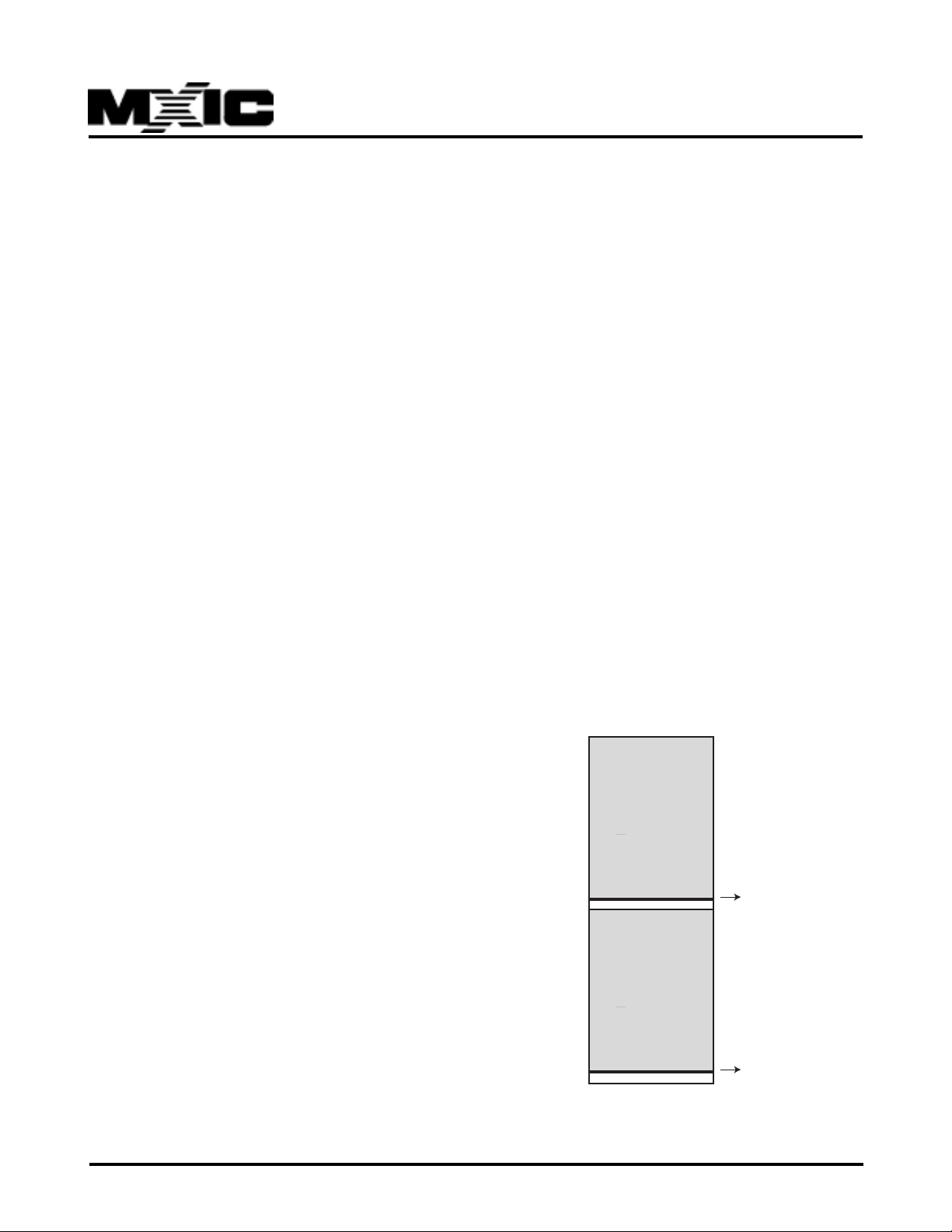
short (* 32 bytes), successive messages, with all additional information can be stored (see Figure6-13).
Characteristic: TEI recognition
A comparison is performed only on the second byte
after the opening flag, with TEI1, TEI2 and group TEI
(FF hex value), and the rest of the frame in the RFIFO.
Additional information is available in the RSTA.
- Transparent mode 2 (MDS2, MDS1, MDS0 = 110)
Characteristic: No address recognition
Every received frame is stored in the RFIFO (first byte
after opening flag to CRC field). Additional information
is available in the RSTA.
P/N:PM0473
0
Receive
Message 1
(< 32 bytes)
31
0
Receive
Message 2
(< 32 bytes)
31
RME
RME
Figure 6-10 Contents of RFIFO (short message)
REV. 2.5, SEP. 05, 2000
29
Page 30
MX97102
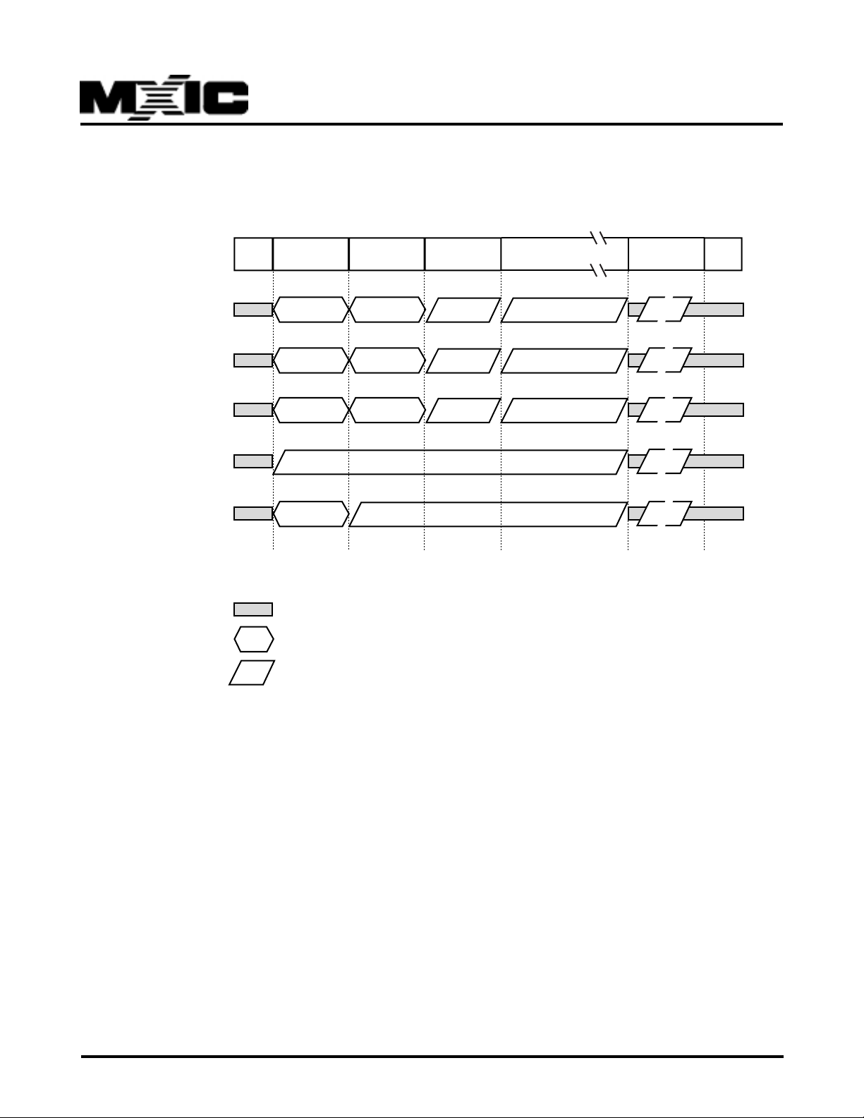
Depending on the message transfer mode the address and control fields of received frames are processed and
stored in the Receive FIFO or in special registers as depicted in Figure 6-11.
Auto-Mode
(U-and I-Frames)
Non-Auto
Mode
Transparent
Mode 1
Transparent
Mode 2
Transparent
Mode 3
Flag
Address
lligh
SAP1,SAP2
FE, FC
(Note 1)
SAP1,SAP2
FE, FC
(Note 1)
SAPR
SAP1,SAP2
FE, FC
Address
Low
TEI1, TEI2
FF
(Note 2)
TEI1, TEI2
FF
(Note 2)
TEI1, TEI2
FF
Symbol Descriptions
:Checked automatically by MX97102
:Compared with Register or Fixed Value
RHCR
(Note 3)
RHCR
(Note 4)
RHCR
(Note 4)
RFIFO
Control
RFIFO
Information
RFIFO
RFIFO
RFIFO
CRC
RSTA
RSTA
RSTA
RSTA
RSTA
Flag
:Stored Information Register or RFIFO
Figure 6-11 Receive Data Flow
Note 1: Only if a 2-byte address field is defined (MDS0=1 in MODE register).
Note 2: Comparison with Group TEI is only made if a 2-byte address field is defined (MDS0=1).
Note 3: In the case of an extended, modulo 128 control field format (MCS=1 in SAP2 register) the control field is
stored in the RHCR in compressed form (I frames).
Note 4: In the case of extended control field, only the first byte is stored in the RHCR, the second in the RFIFO.
P/N:PM0473
30
REV. 2.5, SEP. 05, 2000
Page 31
MX97102
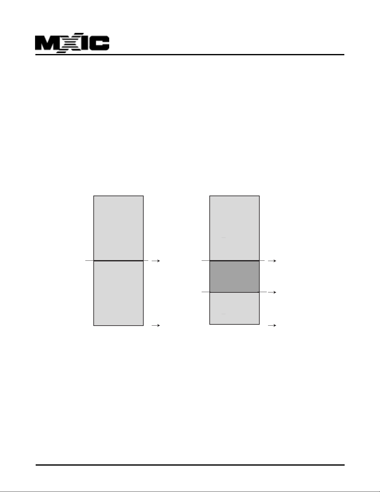
When 32 bytes of a message longer than that are stored
in the RFIFO, the CPU is prompted to read out the
data by an RPF interrupt. The CPU must handle this
interrupt before more than 32 additional bytes are received, which would cause a "data ov erflo w", This corresponds to a maximum CPU reaction time of 16ms
(data rate 16 kbit/s).
After a remaining block of less than or equal to 16 b ytes
has been stored, it is possible to store the first 16 bytes
of a new message (see Figure6-12). The internal
memory is now full. The arrival of additional bytes will
result in "data overflow" (RSTA: RDO) and a third new
RFIFO
0
Long
Message
message in "frame overflo w" (EXIR: RFO). The generated interrupts are inserted together with all additional
information into a queue to be individually passed to
the CPU.
After an RPF or RME interrupt has been processed,
i.e. the received data has been read from the RFIFO,
this must be explicitly acknowledged by the CPU issuing an RMC (Receive Message Complete) command.
The MX97102 can then release the associated FIFO
pool for new data. If there is an additional interr upt in
the queue it will be generated after the RMC
acknowledgement.
RFIFO
0
Receive
Message 1
(< 48 bytes)
31
0
31
RPF
RPF
Figure 6-12 Contents of the RFIFO (long messages)
Transmission of Frames
A 2*32 byte FIFO buffer (transmit pools) is provided in
the transmit direction. If the transmit pool is ready (which
is true after an XPR interrupt or if the XFW bit in STAR
is set), the CPU can write a data block of up to 32
bytes to the transmit FIFO. After this, data transmission can be initiated by command.
31
0
15
16
Message 2
(< 32 bytes)
31
RPF
RME
RME
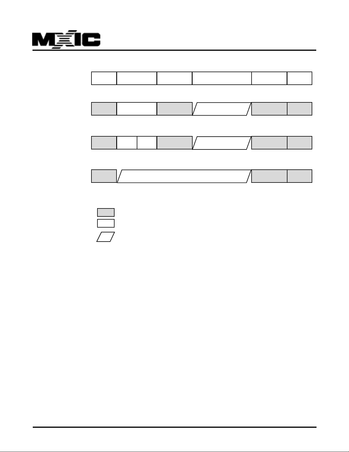
Two different frames types can be transmitted : Transparent frame (command: XTF) or
I frames (command: XIF) as shown in Figure6-16. For transparent frames, the whole
frame including address and control field
must be written to the XFIFO.
P/N:PM0473
REV. 2.5, SEP. 05, 2000
31
Page 32
MX97102
HDLC Frame
Transmit I-Frame
(XIF)
Auto Mode, 8-Bit Addr.
Transmit I-Frame
(XIF)
Auto Mode, 16-Bit Addr.
Transmit Transparent
Frame(XTF)
All Modes
Flag
Flag
Flag XAD1 XAD2
Flag
Address Control
XAD1 Control
Control
Information
XFIFO
XFIFO
XFIFO
Symbol Descriptions
:Generated automatically by MX97102
:Written initially by CPU (Info Register)
:Loaded (repeatedly) by CPU upon MX97102 request (XPR interrupt)
CRC
CRC
CRC
CRC
Flag
Flag
Flag
Flag
Note: Length of Control Field is 8 or 16 Bit
Figure 6-13 Transmit Data Flow
P/N:PM0473
REV. 2.5, SEP. 05, 2000
32
Page 33

MX97102
If a 2-byte address field has been selected, the
MX97102 takes the contents of the XAD1 register to
build the high byte of the address field, and the XAD2
register to build to low byte of the address field. Additionally the C/R bit (bit 1of the high byte address, as
defined by LAPD protocol ) is set to "1" or "0" dependent on whether the frame is a command or a response.
In the case of a 1 byte address, the MX97102 takes
either the XAD1 or XAD2 register to differentiate between command or response frame (as defined by X.25
LAPB).
The control field is also generated by the MX97102 including the receive and send sequence number and
the poll/final (P/F) bit. For this purpose, the MX97102
internally manages send and receive sequence number counters.
In the auto-mode, S frames are sent autonomously by
the MX97102. The transmission of U frames, how ever,
must be done by the CPU. U frames must be sent as
transparent frames (CMDR: XTF), i.e. address and control field must be defined by the CPU. Once the data
transmission has been initiated by command (CMDR:
XTF or XIF), the data transfer between CPU and the
MX97102 is controlled by interrupts.
The MX97102 repeatedly requests another data packet
or block by means of an ISTA:XPR interrupt, every time
no more than 32 bytes are stored in the XFIFO. The
processor can then write further data to the XFIFO and
enable the continuation of frame transmission by issuing an XIT/XTF command. If the data block which has
been written last to the XFIFO completes the current
frame, this must be indicated additionally by setting the
XME (Transmit Message End) command bit. The
MX97102 then terminates the frame properly by appending the CRC and closing flag.
causes an XPR interrupt.
After an end of message indication from the CPU
(CMDR: XME command), the termination of the transmission operation is indicated differently, depending on
the selected message transfer mode and the transmitted frame type.
If the MX97102 is operating in the auto mode, the window size is limited to"1"; therefore an ackno wledgement
may be provided either b y a received S or I frame with
corresponding receive sequence number. If no
acknowledgement is receiv ed within a certain time (programmable), the MX97102 requests an
acknowledgement by sending an S frame with the poll
bit set (P=1) (RR or RNR). If no response is received
again, this process is repeated in total N2 times (retry
count, programmable via TIMR register).
The termination of the transmission operation may be
indicated either with:
- XPR interrupt, if a positive acknowledgement has been
received,
- XMR interrupt, if a negative acknowledgement had
been received, i.e. the transmitted message must be
repeated (XMR = Transmit Message Repeat),
- TIN interrupt, if no acknowledgement has been received at all after N2 times the expiration of the time
period t1 (TIN = Timer INterrupt, XPR interrupt is issued additionally).
Note: Prerequisite f or sending I frames in the auto-mode
(XIF) is that the internal operational mode of the timer
has been selected in the MODE register (TMD bit = 1).
The transparent transmission of frames (XTF command)
is possible in all message transfer mode. The successful termination of a transparent transmission is indicated
by an XPR interrupt.
If the CPU fails to respond to an XPR interrupt within
the given reaction time, a data underrun condition occurs (XFIFO holds no further valid data). In this case,
the MX97102 automatically aborts the current frame
by sending seven consecutive "ones" (ABORT sequence). And the CPU is informed about this via an
XDU (Transmit Data Underrun) interrupt. It is also possible to abort a message by software by issuing a
CMDR:XRES (Transmitter Reset) command, which
P/N:PM0473
In all cases, collisions which occur on the S-Bus (D
channel) before the first XFIFO pool has been completely transmitted and released are treated without
CPU interaction. The MX97102 will retransmit the fr ame
automatically . If a collision is detected after the first pool
has been released, the MX97102 aborts the frame and
requests the processor to repeat the frame with an XMR
interrupt.
REV. 2.5, SEP. 05, 2000
33
Page 34
Interrupt Structure and Logic
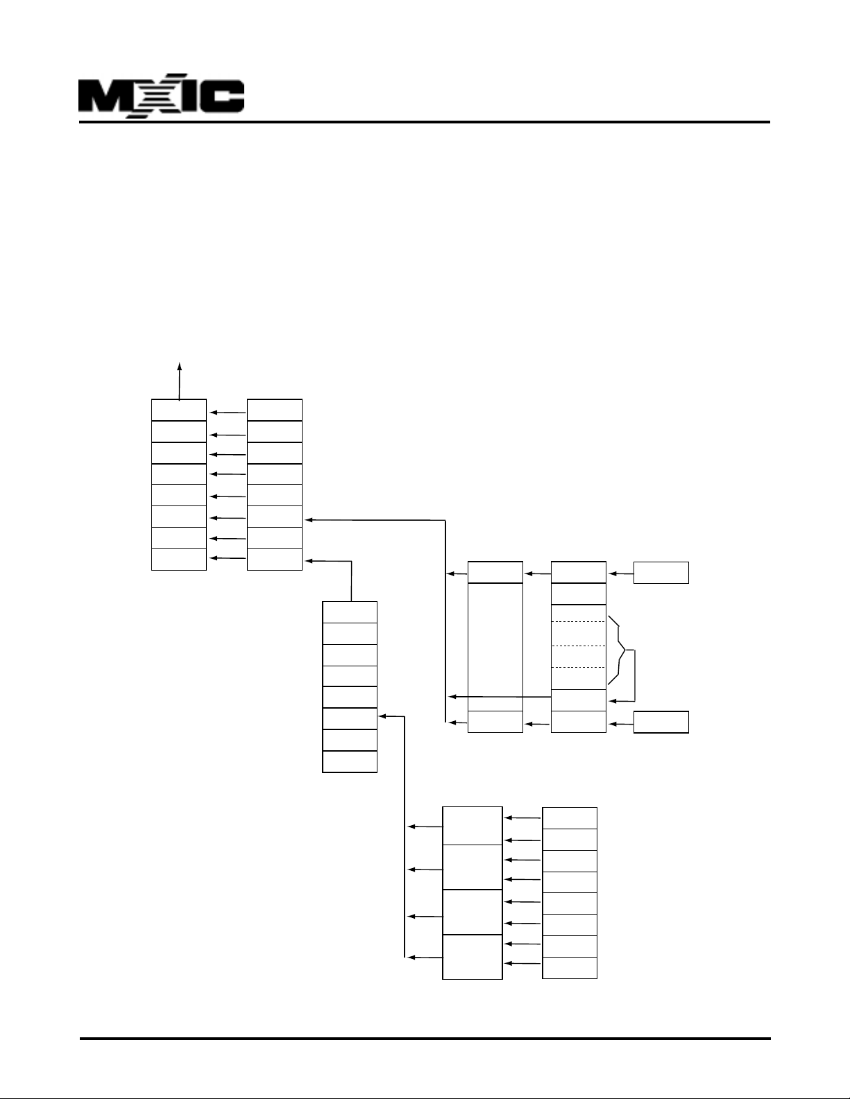
Since the MX97102 provides only one interrupt request
output (INT), the cause of an interrupt is determined by
the microprocessor by reading the Interrupt Status Register (IST A). In this register , sev en interrupt sources can
be directly read. The LSB of the ISTA points to eight
non-critical interrupt sources which are indicated in the
Extend Interrupt Register (EXIR). Figure6-16 shows the
MX97102 interrupt structure.
INT
MX97102
RME
RPF
RSC
XPR
TIN
CISQ
SIN
EXI
MASK
RME
RPF
RSC
XPR
TIN
CISQ
SIN
EXI
ISTA
XMR
XDU
PCE
RFO
SOV
MOS
SAW
WOV
EXIR
SQIE SQC SQRR
BAS
C
O
D
R
0
CIC0
CI1E
SQXR
MRE1
MXE1
MRE0
MXE0
CIR0
MOSRMOCR
MDR1
MER1
MDA1
MAB1
MDR0
MER0
MDA0
MAB0
CIR1CIC1
P/N:PM0473
Figure6-14 MX97102 Interrupt Structure
REV. 2.5, SEP. 05, 2000
34
Page 35

MX97102
A read of the ISTA register clears all bits expect EXI
and CISQ. CISQ is cleared by reading CIR0.
A read of EXIR clears the EXI bit in ISTA as well as the
EXIR register. When all bits in ISTA are cleared, the
interrupt line (PINTN) in deactivated.
Each interrupt source in ISTA register can be selectively masked b y setting to “1” the corresponding bit in
MASK. Masked interrupt status bits are not indicated
when IST A is read. Instead, they remain internally stored
and pending, until the mask bit is reset to zero. Reading the ISTA while a mask bit is active has no effect on
the pending interrupt.
In the event of an extended interrupt and of a C/I or S/
Q channel change, EXI and CISQ are set even when
the corresponding mask bits in MASK are active, but
no interrupt (INT) is generated. Except for CISQ and
MOS all interrupt sources are directly determined by a
read of ISTA and (possibly) EXIR.
A CISQ interrupt may originate from a change in the
received S/Q code (SQC), from a change in the received C/I channel 0 code (CIC0) or form a change in
the received C/I channel 1 code (CIC1).These three
corresponding status bits SQC, CIC0 and CIC1 are read
then cleared in the CIR0 register. SQC and CIC1 can
be individually disabled by clearing the enable bit SQIE
(SQXR register) or, respectively, CI1E (SQXR register).
An interrupt status is indicated every time a valid new
code is loaded in SQRR, CIR0 or CIR1. But in case of
a code change, the new code is not loaded until the
previous contents have been read. When this is done
and a second code change has already occurred, a
new interrupt is immediately generated and the new
code replaces the previous one in the register . The code
registers are buffered with a FIFO size of two. Thus, if
several consecutive codes are detected, only the first
and the last code is obtained at the first and second
register read, respectively.
The MONITOR Data Receive (MDR) and the MONITOR End of Reception (MER) interrupt status bits hav e
two enable bits, MONITOR Receive interrupt Enable
(MRE) and MR bit Control (MRC). The MONIT OR channel Data Acknowledged (MDA) and MONITOR channel Data Abort (MAB) interrupt status bits have a common enable bit MONITOR Interrupt Enable (MXE).
MRE prevents the occurrence of the MDR status, including when the first byte of a packet is receiv ed, When
MRE is active (1) but MRC is inactive, the MDR-interrupt status is generated only for the first byte of a receive packet. When both MRE and MRC are active,
MDR is generated and all received monitor bytes marked by a 1-to-0 transition in MX bit - are stored.
The INT output is level active. It stays active until all
interrupt sources have been serviced. If a new status
bit is set while an interrupt serviced, the INT line stays
active. This ma y cause problem if the MX97102 is connected to edge-triggered interrupt controllers. To avoid
these problems, it is recommended to mask all interrupts at the end of the interrupt service program and to
enable the interrupts again. This is done by writing FF
hex value to the MASK register and to write back the
old value of the MASK register.
P/N:PM0473
REV. 2.5, SEP. 05, 2000
35
Page 36
MICROPROCESSOR INTERFACE CONNECTION
MX97102
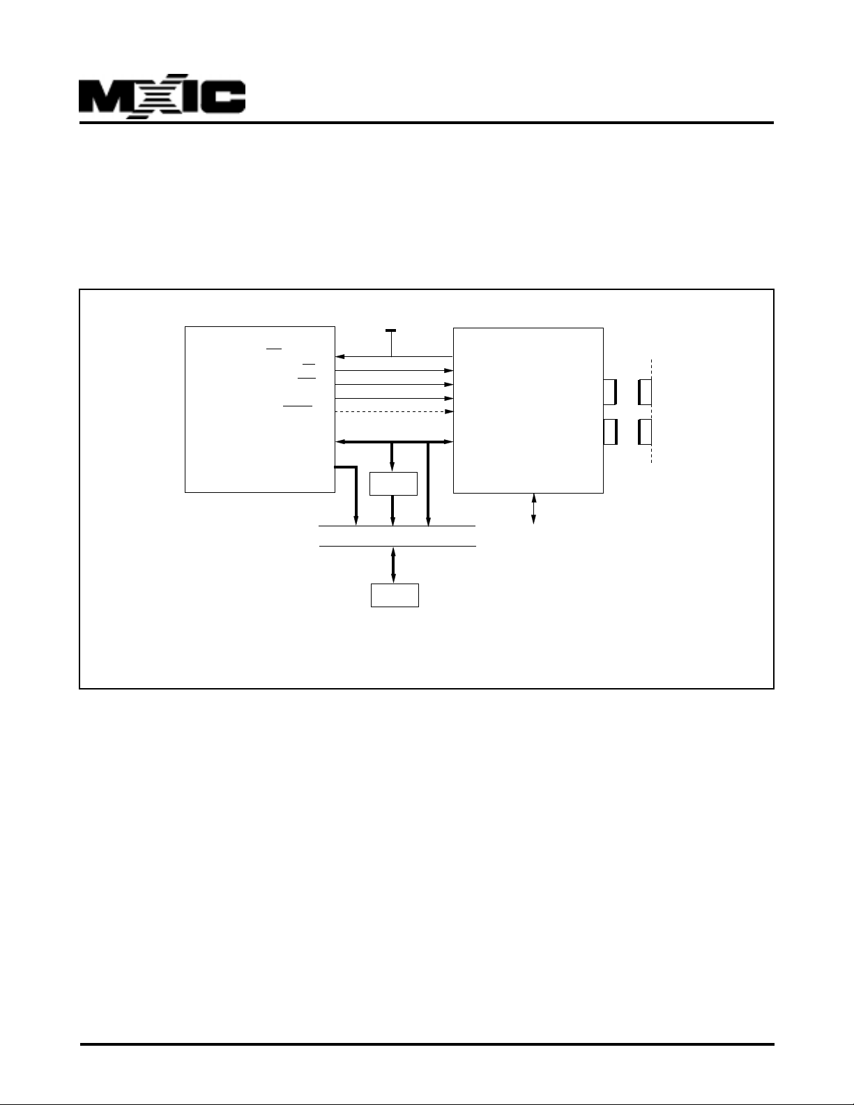
Single-chip microcontroller, such as 8048, 8031 or 8051,
can meet the need of MX97102. MX97102 is built in
various microprocessor interface, it fits perfectly into
almost any 8-bit microprocessor system environment.
The microprocessor interface can be selected to be ei-
+5V
INT(INTX)
RD
WR
80C51
(80C188)
ALE
(PSCX)
AD7....AD0
A15....A8
Latch
Common Bus A15-A0, D7-D0
Memory
ther of the Motorola type (with control signals CS, R/W ,
DS) of the Siemens/Intel non-multiplex ed bus type (with
control signals CS, WR, RD) or of the Siemens/Intel
multiplex ed address/data bus type (with WR, RD , ALE).
PINTN
PRDN
PWRN
PALE
PCSN
PAD7....0
PSX1
PSX2
PSR1
PSR2
MX97102
GCI
S
P/N:PM0473
FIGURE 7: CONNECTING THE MX97102 TO INTEL MICROCONTROLLER
REV. 2.5, SEP. 05, 2000
36
Page 37
S/T INTERFACE
MX97102
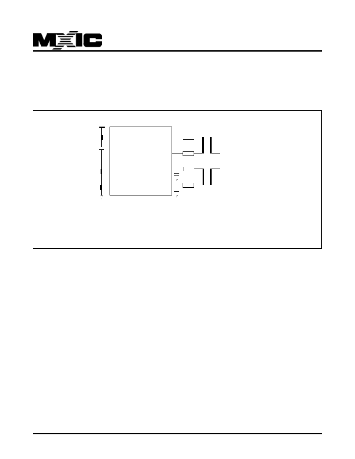
Line transceiver functions for the S/T interface follows
the electrical specifications of CCITTI.430. According
to this standard, pseudo-ternary encoding with 100%
pulse width is used on the S/T interface. For both re-
+5V
VDD
10uf
MX97102
VSSD
VSSA
GND
PSX1
PSX2
PSR1
PSR2
FIGURE 8: MX97102 EXTERNAL S-INTERFACE CIRCUITRY
ceive and transmit direction, a 2:1 transformer is used
to connect the MX97102 transceiver to the 4 wire S/T
interface.
2 : 1
Transmit Pair
2 : 1
Receive Pair
Protection Circuits
( * please see the Application note, PM 0624)
The receiver is changed as a threshold detector with
adaptively switched threshold levels. Pin PSR1 delivers 2.5V as an output, which is the virtual ground of the
input signal on pin PSR2.
E-channel Monitoring
This feature is provided by two ways, one way is to
allow cpu to access two serial E-bits in a register, the
other way is to get the E-bit signal from one pin of this
chip. (please see Application Note PM0624 for details .)
SDSX Programming
Strobes 1 and 2 are provided, please see the Application Note for defails.
P/N:PM0473
REV. 2.5, SEP. 05, 2000
37
Page 38

MX97102
INTERNAL REGISTER
TABLE 8 : HDLC OPERATION AND STATUS REGISTERS
Addr. Name R/W Bit7 Bit6 Bit5 Bit4 Bit3 Bit2 Bit1 Bit0 Descr iption
(hex)
00-1F FIFO R/W Tx/Rx FIFO address
20 ISTA R RME RPF RSC XPR TIN CISQ SIN EXI Interr upt Status Register
20 MASK W RME RPF RSC XPR TIN CISQ SIN EXI Mask Register
21 STAR R XDOV XFW XRNR RRNR MBR MAC1 X MAC0 Status Register
21 CMDR W RMC RRES RNR STI XTF XIF XME XRES Command Register
22 MODE R/W MDS2 MDS1 MDS0 TMD RAC DIM2 DIM1 DIM0 Mode Register
23 TIMR R/W CNT CNT CNT V A L U E Timer Register
24 EXIR R XMR XDU PCE RFO SOV MO S SAW WOV Extended Interrupt
Register
24 XAD1 W Transmit Address 1
25 RBCL R RBC7 RBC6 RBC5 RBC4 RBC3 RBC2 RBC1 RBC0 Receive Frame
Byte Count Low
25 XAD2 W Transmit Address 2
26 SAPR R Received SAPI
26 SAP1 W SAPI1 SAPI1 SAPI1 SAPI1 SAPI1 SAPI1 CRI 0 Individual SAPI 1
27 RSTA R RDA RDO CRC RAB SA1 SA0 C /R TA Receive Status Register
27 SAP2 W SAPI2 SAPI2 SAPI2 SAPI2 SAPI2 SAPI2 MCS 0 Individual SAPI 2
28 TEI1 W TEI1 TEI1 TEI1 TEI1 TEI1 TEI1 TEI1 EA Individual TEI 1
29 RHCR R Receive HDLC Control
29 TEI2 W TEI2 TEI2 TEI2 TEI2 TEI2 TEI2 TEI2 EA Individual TEI 2
2A RBCH R XAC VN1 VN0 OV RBC11 RBC10 RBC9 RBC8 Receive F ram Byte Count
High
2B STAR2 R 0 0 0 0 WFA MULT TREC SDET Status Register 2
2B STAR2 W 0 0 0 0 0 MULT 0 0 Status Register 2
P/N:PM0473
REV. 2.5, SEP. 05, 2000
38
Page 39

MX97102
TABLE 9 : SPECIAL PURPOSE REGISTERS
Addr. Name R/W Bit7 Bit6 Bit5 Bit4 Bit3 Bit2 Bit1 Bit0 Description
(hex)
30 SPCR R/W SPU 0 0 TLP C1C1 C1C0 C2C1 C2C0 Serial Port Control Reg.
31 CIR0 R SQC BAS CODR0 CODR0 CODR0 CODR0 CIC0 CIC1 Command/Indication
Receive 0
31 CIX0 W RSS BA C CODX0 CODX0 CODX0 CODX0 1 1 Command/Indication
T ransmit 0
32 MOR0 R MONITOR Receive 0
32 MOX0 W MONIT OR T ransmit 0
33 CIR1 R CODR1 CODR1 CODR1 CODR1 CODR1 CODR1 MR1 MX1 Command/Indication
Receive 1
33 CIX1 W CODX1 CODX1 CODX1 CODX1 CODX1 CODX1 1 1 Command/Indication
T ransmit 1
34 MOR1 R MONITOR Receive 1
34 MOX1 W MONIT OR T ransmit 1
35 C1R R/W Channel Register 1
36 C2R R/W Channel Register 2
37 B1CR R B1-Channel Register
37 STCR W TSF TBA2 TBA1 TBA0 ST1 ST0 SC1 SC0 Sync Tr ansfer Control
Register
38 B2CR R B2-Channel Register
38 ADF1 W WTC1 WTC2 TEM PFS IOF 0 0 ITF Additional Feature Reg.1
39 ADF2 R/W IMS 0 0 0 ODS D1C2 D1C1 D1C0 Additional Feature Reg.2
3A MOSR R MDR1 MER1 MDA1 MAB1 MDR0 MER0 MDA0 MAB0 MONITOR Status Reg.
3A MOCR W MRE1 MRC1 MXE1 MXC1 MRE0 MRC0 MXE0 MXC0 MONITOR Control Reg.
3B SQRR R IDC CFS CI1E SYN SQR1 SQR2 SQR3 SQR4 S-,Q-Channel Receive
Register
3B SQXR W IDC CFS CI1E SQIE SQX1 SQX2 SQX3 SQX4 S-,Q-Channel Transmit
Register
3C ADF3 R/W 0 0 0 1 STM1 STM0 MAX1 MAX0 Additional Feature Reg.3
3D EMR R 0 0 0 0 0 0 EMR1 EMR0 E-channel bits reg.
3D EDR W 0 0 0 0 D_SIZER0 D_SFLAGS D_UNARB EMON D/E channel Control reg.
3E ADF4 R/W IMS 0 0 0 BFWD D2C2 D2C1 D2C0 B-exchang, SDS2 reg.
ORDERING INFORMATION
PART NO. PACKAGE
MX97102QC 44 PIN PLCC
MX97102UC 64 PIN LQFP
P/N:PM0473
REV. 2.5, SEP. 05, 2000
39
Page 40

MX97102
REVISION HISTORY
Rev. No. Description Page Date
1.1 Preliminary release JULY/28/1997
1.2 Change editing NOV/1997
Add ordering information and revision history
Change words in drawings
Add "not used" pins in pin descriptions
1.3 Page6, Table 3 changed NOV/1997
1.4 Wording errors APR/14/1998
1.5 Change feature description MAY/21/1998
1.6 Storage Temperature Range " -65°C to 125°C" replaced by "-55°C to 150°C" P4 JUN./15/1998
1.7 Add 64-pin package AUG/21/1998
1.8 Made for CD-ROM release SEP/15/1998
1.9 Modify 64-pin package outline data OCT/20/1998
2.0 64 PIN P-LQFP PACKAGE INFORMATION content changed P16 OCT/27/1998
2.1 New revision adds E-channel monitoring function, extra SDS2 pin P1,3,4, APR/01/1999
2.2 Add one E-bit pin P10~35 DEC/17/1999
Add LQFP pin description
Revise figure 8
Add LQFP package data
Add more descriptions
2.3 Add Pre-Filter Compensation P22 JAN/21/2000
2.4 Contents modify P5,8 APR/28/2000
2.5 Modify state diagram 6-9(a)&6-9(b) P23,24 SEP/05/2000
P/N:PM0473
REV. 2.5, SEP. 05, 2000
40
Page 41
PACKAGE INFORMATION
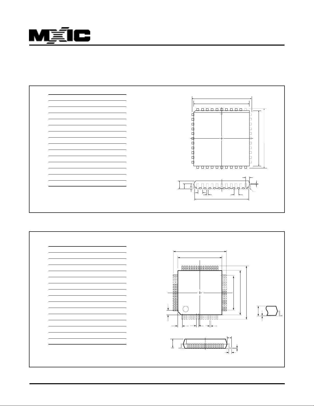
44-PIN PLASTIC LEADED CHIP CARRIER (PLCC)
MX97102
ITEM MILLIMETERS INCHES
A 17.53 ± .12 .699 ± .005
B 16.59 ± .12 .653 ± .12
C 16.59 ± .12 .653 ± .12
D 17.53 ± .12 .690 ± .12
E 1.95 .077
F 4.70 max. .185 max.
G 2.55 ± .25 .100 ± .010
H .51 min. .020 min.
I 1.27 [Typ.] .050 [Typ.]
J .71 ± .10 .028 ± .004
K .46 ± .10 .018± .004
L 15.50 ± .51 .610 ± .020
M .53 R .025 R
N .25 [Typ.] .010 [Typ.]
NOTE: Each lead centerline is located within .25
mm[.01 inch] of its true position [TP] at
maximum material condition.
F
G
64-PIN PLASTIC LOW-PROFILE QUAD FLAT PACKAGE (P-LQFP)
A
B
64044
7
13
17
18 28
H
I
1
23
K
L
39
CD
33
29
E
N
M
J
P/N:PM0473
ITEM MILLIMETERS INCHES
A 16 .63
B 14 .55
C 14 .55
D 16 .63
E 12 [Typ.] .47 [Typ.]
F 1 [Typ.] .039 [Typ.]
G 1 [Typ.] .039 [Typ.]
H .35 ± .05 .014 ± .002
I 0.8 .031
J 1 .039
K .6 ± .15 .024± .006
L .15 ± .05 .006 ± .002
M 1.4 ± .05 .057 ± .002
N .1 ± .05 .004 ± .002
O 1.6 [max.] .063 [max.]
NOTE: Each lead centerline is located within .25
mm[.01 inch] of its true position [TP] at
maximum material condition.
41
A
B
CD
E
F
IHG
M
J
K
O
N
L
REV. 2.5, SEP. 05, 2000
Page 42

MX97102
MACRONIX INTERNATIONAL CO., LTD.
HEADQUARTERS:
TEL:+886-3-578-6688
FAX:+886-3-563-2888
EUROPE OFFICE:
TEL:+32-2-456-8020
FAX:+32-2-456-8021
JAPAN OFFICE:
TEL:+81-44-246-9100
FAX:+81-44-246-9105
SINGAPORE OFFICE:
TEL:+65-348-8385
FAX:+65-348-8096
TAIPEI OFFICE:
TEL:+886-2-2509-3300
FAX:+886-2-2509-2200
MACRONIX AMERICA, INC.
TEL:+1-408-453-8088
FAX:+1-408-453-8488
CHICAGO OFFICE:
TEL:+1-847-963-1900
FAX:+1-847-963-1909
http : //www.macronix.com
MACRONIX INTERNATIONAL CO., LTD. reserves the right to change product and specifications without notice.
42
 Loading...