

Page 1

1. INTRODUCTION
The purpose of this application note is to describe the
Implementation of a generic bus 100Base-TX Fast
Ethernet node using MXIC highly integrated single chip
Fast Ethernet controller MX98728EC series. Most description in this application note applied to both
MX98728EC and MX98728AEC unless specifically described for different chips. MX98728EC in this application note refer to both MX98728EC and MX98728AEC
for common descriptions. This document presents product overview , programming guide and hardware design
guidelines. It is recommended that you are familiar with
the data sheet of MX98728EC or MX98728AEC before
using this guide.
2. PRODUCT OVERVIEW
The MX98728EC implements the 10/100Mbps MAC and
Physical layer on single chip in accordance with the IEEE
802.3 standard.
PRELIMINARY
MX98728EC
APPLICATION NOTE
The MX98728EC highly integrates with direct host bus
interface, including host bus slave with burst read transfer, direct EEPROM interface ( optional), and large on
chip transmit/receive FIFOs. Also , the MX98728EC is
equipped with intelligent IEEE802.3u compliant Nway
auto-negotiation capability allowing a single RJ-45 connector to link with the other IEEE802.3u compliant device without re-configuration. For detailed product specification information, please refer to the Data sheet of
MX98728EC.
MII (Media Independent Interface) Connection is
provided by MX98728EC and MX98728AEC as an
option to work with third party 10/100 fast Ethernet
tranceiver or ev en Home PNA tranceiv er . P ossible
system application can allow integration of both
Ethernet and Home PNA network in a single system.
P/N:PM0599
REV. 0.6, JUN. 22, 2000
1
Page 2
3. HARDWARE DESIGN CONSIDERATIONS
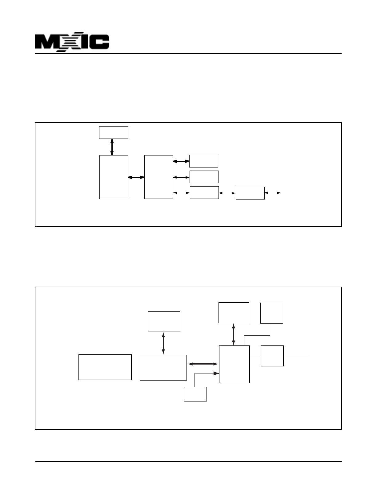
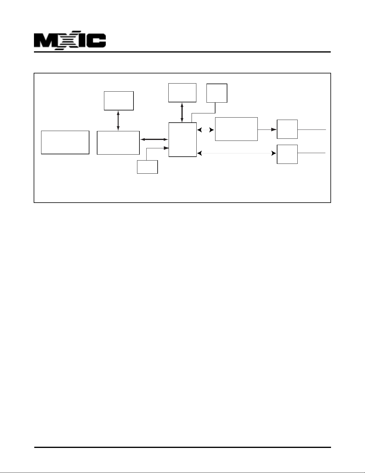
3.1 System Application Block Diagram
A System block diagr am for the MX98728EC based F ast
Ethernet is shown as following.:
Host memory
Host
Customer
Applicatio
MX98728EC
Packet buffer
EEPROM
MX98728EC
Optional
*
*
Typical Application
Customer Application
Magnetic
SYSTEM APPLICATION BLOCK DIAGRAM
Packet
Host Memory
Subsystem
Local DMA
Host
CSB
buffer
MX98728EC
RJ45
EPROM
C46/C66
RJ45
Xformer
TP cable
Decode
TYPICAL APPLICATION
P/N:PM0599 REV. 0.6, JUN. 22, 2000
2
Page 3
Combo Application
MX98728EC
Host Memory
Customer Application
Subsystem
Host
Decode
Local DMA
MX98728EC
CSB
COMBO APPLICATION
3.2 System Through Put Considerations
Total system through put is determined by several factors, namely, packet memory through put, host bus
through put, and local DMA through put. MX98728EC is
designed to achieve maximum network through put possible in a 100 TX mode with full duplex operation. The
maximum data rate of a full line speed 100M bits /s
Ethernet is roughly 12.5MB/s in half duplex mode and
25MB/s for full duplex mode when IPG is 960ns and all
ethernet packet length is 1518 bytes.
To achieve such high through put, bandwidth requirements for packet memory are as follows :
1.Host <- GMAC <- P acket Memory >=12.5MB/s for RX
2.Host -> GMAC -> P ac k et Memory ( or TX FIFO )
>= 12.5MB/s for TX
3.Network -> GMAC -> Pac k et Memory >= 12.5MB/s
for RX channel
4.Network <- GMAC <- P ack et Memory ( or TX FIFO )
>= 12.5MB/s for TX channel
The total maximum bandwidth of pac k et memory is
50Mhz/2 x 2B = 50MB/s for 16-bit mode
50Mhz/2 x B = 25MB/s for 8-bit mode
Packet
buffer
EPROM
C46/C66
or
1M 8PHY
or
10M 8PHY
RJ11
Xformer
RJ45
Xformer
How to get most throughput in 8-bit packet memory mode
?
If we use TX DMA mode for transmission, then to
achieve full duplex line speed, it will need 12.5MB x 4 =
50MB for all host DMA and GMAC's local DMA. Obviously, 8-bit packet memory does not have so much
throughput. Instead, we must use TX FIFO mode for
transmission, which will require only 12.5MB x 2 of packet
memory to achieve RX's line speed ( assuming that software can deliver the same throughput as well ).
TX FIFO mode does not use packet memory to
store TX pac ket for transmission, therefore RX DMA can
use all 8-bit packet memory bandwidth which is 25MB.
Since GMAC can do "seamless" local DMA cycles, i.e.
every 40ns one packet memory transfer is processed,
no cycle is wasted for bus arbitrations. Also the on-chip
burst read buffer will constantly filling up the 4 word ( 4
dword ) buffer whenever this buffer is not full ( 4 word, or
4 dword ).
Also to maximize TX FIFO throughput will require some serious software intelligence. i.e. software
must fill up TX FIFO as much as possible during the
IPG time ( 960ns ) in order to achieve more outgoing
data.
Phone Line
TP cable
P/N:PM0599 REV. 0.6, JUN. 22, 2000
3
Page 4

MX98728EC
3.3 CPU Bus connection
The MX98728EC provides direct Generic b us interface
to host bus. Hardware designers should especially take
care of the D[31:0], A[15:0], SRDY, RDB, WRB, INTB,
DREQB, D ACKB, RSTB , CSB, and H16_32.
3.4 OSCILLA TOR/CR YST AL
CKREF (X1), and X2: The MX98728EC is designed to
operate with 25MHz oscillator or crystal module. The
clock specification of this oscillator or crystal should
meet 25Mhz +/- 30PPM. See Appendix A for more details.
3.5 Optional Serial EEPROM
The MX98728EC provides pins EECS, MA2(EEDO),
MA1(EEDI), MA0(EECK), and C46/C66 for directly accessing the serial EEPROM. The contents of EEPROM
includes MAC the ID information of the MX98728EC and
the configuration parameters for software dr iver. The
EEPROM contents should follow the definition in this
application note.
3.6 LED support
The MX98728EC provides two pins LED0 and LED1 to
control display LEDs. Displayed messages are as follows:
LED0: Speed LED , which light is on, it indicates 100Mbps
speed. When off indicates 10Mbps speed.
LED1: Link/Activity LED, when light is stable and on, it
indicates good link. When flashing, indicates TX or RX
activities. When off means bad link.
3.7 Network interface to Magnetic component
For isolating and impedance matching purpose, an isolating transformer with 1:1 transmit and 1:1 receive turns
ratio is required for transmit and receive twisted pair interface. In Appendix A, several transformers that we had
verified successfully.
3.8 MII Interface
MDC and MDIO pin should be both externally pull down
(4.7K) for application that use MII interface to connect
to external tranceiver. If MII interface is not used, both
MDC and MDIO must be grounded or pulled down.
P/N:PM0599 REV. 0.6, JUN. 22, 2000
4.0 Driver Programming Guide
4.1 Hardware reset.
The hardware reset is applied to the MX98728EC's RSTB
pin. The MX98728EC starts to access the commands
from Host after 400ms. In other hands, MX98728EC
starts to access the commands after 400ms from RSTB
pin goes high. Because that it takes time for the analog
transceiver to be initialized.
4.2 Registers Initialization
The MX98728EC must be initialized prior to transmission or reception of packets from the network. The default register content after hardware reset are listed below :
Reg0h:00h
Reg1h:01h
Reg2h:00h
Reg3h:00h(T est Register , not used by software)
Reg4h:xxh(Read only)
Reg5h:xxh(Read only)
Reg7h,6h:0000h
Reg8h:00h
Reg9h:00h
Reg0B,0Ah:x000h
Reg0D ,0Ch:x000h
Reg0F,0Eh:x000h
Reg11,10h:x000h(reserved)
Reg13,12h:x000h
Reg15,14h:0000h
Reg17,16h:x000h
Reg19,18h:0000h
Reg1B,1Ah:x000h
Reg1Ch:00h
Reg1Dh:00h
Reg1F,1Eh:x000h
Reg20~25h:00h
Reg26~2Dh:00h
Reg2Eh:07h(tranceiver option bits)
Reg2Fh:00h
Reg30h:84h(NWAY is in automatic mode)
Reg31h:a valid network mode (Read only)
Reg32h:00h
Reg33h:00h
Reg37~34h:xxxxxxxxh(write only port)
Reg39,38h:0000h
Reg3A:00h
Reg3B:Link Partner's Status(read only)
Reg3C:00h
Reg3D:3Ch
Reg3F/3E:x000h
4
Page 5

MX98728EC
Reg40~4h:xxxxxxxxh(write only)
Reg45,44h:"MX"(read only)
Reg47,46:"0001"(read only)
Reg4B~4h:xxxxxxxxh(write only)
Reg4F~4h:xxxxxxxxh(write only)
Reg50h:00h
Reg53,52h:0000h(read only)
Set the value in Register IMR Reg08h, for desirable interrupts.
4.3 T ransmit Initialization
1.Allocate the memory for Transmit buffer r ing by programming TLBP and to desired page within the packet
memory. Set TWP and TRP to TLBP page.
2.Set the threshold level which is defined by GCB register TTHD[1:0] or use the def ault value .
4.4 Transmission
1.Write a packet into either the transmit buffer ring or
transmit FIFO.
4.6 Receive Initialization
1.Allocate the memory for receive buffer ring by programming RHBP page register to desired page. Set
RWP and RRP to BP page.
2.Set the threshold level which is defined by RTHD[1:0]
or use the default setup.
3.Set up MAC address in register Reg20-25h if no
EEPROM is used during hardware reset, set up register 26-2Dh for multicast hash table.
4. Programming the desired network address filtering
modes through register 01h.
4.7 Reception
1.Set register bit reg0h.SR bit to enable the reception of
packet.
2.When the first packet begin arriving the MX98728EC
begins to store packet at the location pointed by the
RWP.
2.Issue appropriate transmit command through reg
0h.ST0 and ST1 bits.
3. If a packet transmission is completed, the OWN bit of
current packet's descriptor will be cleared to zero,
and ST0, ST1 bits are internally reset by MX98728EC.
4. F or successful transmission, an interrupt is asserted
by interrupt register bit TI of interrupt register . Driver
can now check Reg04h for last transmission status
or use IORD , IORDP register to read status from transmit descriptor.
4.5 Collision recovery
If the collision is detected before the first 64 bytes of
packet has been transmitted, The FIFO will restore the
necessary FIFO pointers to retransmit the same packet
without fetching the transmitted data from packet
memory.
If After 64 bytes of data transmitted, An out-of window
collision is occurred. This packet will be aborted with
interrupt asserted. OWC bit of transmit descriptor is set
and device driver needs to resolve such situation. And
reissue a transmit command so that MX98728EC can
fetch the entire packet from packet memory again for
retransmission.
3. If a packet is successfully received, MX98728EC will
store the receive status, packet length and next packet
pointer in the receive descriptor located at the beginning of the first page of packet. The status of last descriptor is also stored in the LRPS ( reg05h) .
4.8 Receive Buffer Ring Full
In a heavily loaded network which may cause overflow
of the receive buffer ring, when the last available page
is exhausted and more data needs to be stored for the
current packet then the receive buffer ring is full but
GMAC will continue receiving until RX FIFO is also overflow . At this point, GMAC will do the following actions :
1. Close current received packet with the FO bit ( bit 3 )
and the BF bit ( bit 0 ) of the receive descriptor being
set if a minimum of one page is used by this packet.
2. An interrupt may be asser ted if the RBFI ( register
09h bit 7 ) interrupt bit is set and the RBFIM bit (
register 08h bit 7 ) is also set.
3. If AUTORCVR is set, then the last packet with FO,
BF error will be discarded from the packet memory
and from RX FIFO as well and receiving is resumed
for next packet.
P/N:PM0599 REV. 0.6, JUN. 22, 2000
5
Page 6

MX98728EC
4. If AUTORCVR is reset, then GMAC can not receive
any more packet. All following packets will be lost
and MPC ( Missed Packet Counter ), registers 07h
and 06h, will be increment automatically. MPC can
be reset by the device driver .
If device driver choose AUTORCVR = 0, the following
procedure is suggested for the device driver to recover
from such an error situation manually .
1. Issue the SR=0 ( NCRA register bit 3 ) which will stop
RX channel to prevent new data from coming into RX
FIFO.
2. Issue RX FIFORST to clean RX FIFO.
3. Remo ve all the received pac kets in the packet memory .
When buffer ring is empty, RRP=RWP.
4. Clear all receive related interrupt flags and then set
the SR bit=1 to resume the receive operation.
4.9 Loopback Diagnostics
Three forms of local loopback are provided on the chip.
The user has the ability to loopback through the internal
FIFO, through the internal NW AY logic and through the
internal PMD transceiver. There is also a 4th loopback
which is widely used for board level diagnostic test which
is called external loopback ( off the chip ) using a real
cable with TX end wired back to RX end. The chip is set
up in a full duplex mode to support this external
loopback.
The loopback capabilities are provided to allow customer
to do in site diagnostic or production tests.These
loopbacks verify the following:
1. Internal FIFO loopback ( mode 1 loopback ):
V erify integrity of data path and FIFOs. Receiv ed data
is checked against transmitted data.
Set up loopback operations in MX98728EC:
1.FIFO loopback ( mode 1 ):
Initialize MX98728EC.
Set LB[1:0] = [0,1] in reg 0h. FIFO loopback.
Set up interrupt IMR register.
Fill the pattern to Transmitted buffer .
Enable the Transmission.
Check reception buffer is completed.
Compare the data of reception with Transmitted buff er.
2. NWA Y loopbac k ( mode 2 ):
Initialize MX98728EC.
Set LB[1:0] =[1,0] in reg 0h for internal NWAY loopback.
Set up interrupt IMR register.
Fill the pattern to Transmitted buffer .
Enable the Transmission.
Check reception buffer is completed.
Compare the data of reception with Transmitted buff er.
3. Internal PMD loopback ( mode 3 ) :
Initialize MX98728EC. Set network speed first.
Set LB[1:0] = [1,1] in reg0h for internal PMD loopback.
Set up interrupt IMR register.
Fill the pattern to Transmitted buffer .
Enable the Transmission.
Check reception buffer is completed.
Compare the data of reception with Transmitted buff er.
4. External loopback ( normal mode in full duplex ) :
Initialize MX98728EC. Set network speed first.
Set LB[1:0] = [0,0] in reg0h for normal mode.
Set FD bit =1 in register30.0 for full duplex.
Set up interrupt IMR register.
Fill the pattern to Transmitted buffer .
Enable the Transmission.
Check reception buffer is completed.
Compare the data of reception with Transmitted buff er.
2. Internal NW AY loopback ( mode 2 loopback ):
V erify 5B/4B interface , scramb le/descr amble logic ,
serial to parallel interface logic.
3. Internal PMD loopback ( mode 3 loopback):
V erify tranceiver's functionality and fundamental transmit and receive logic.
4. External loopback ( normal mode in full duplex):
Verify FIFO, Nwa y and PMD all at the same
time.
P/N:PM0599 REV. 0.6, JUN. 22, 2000
6
Page 7
MX98728EC
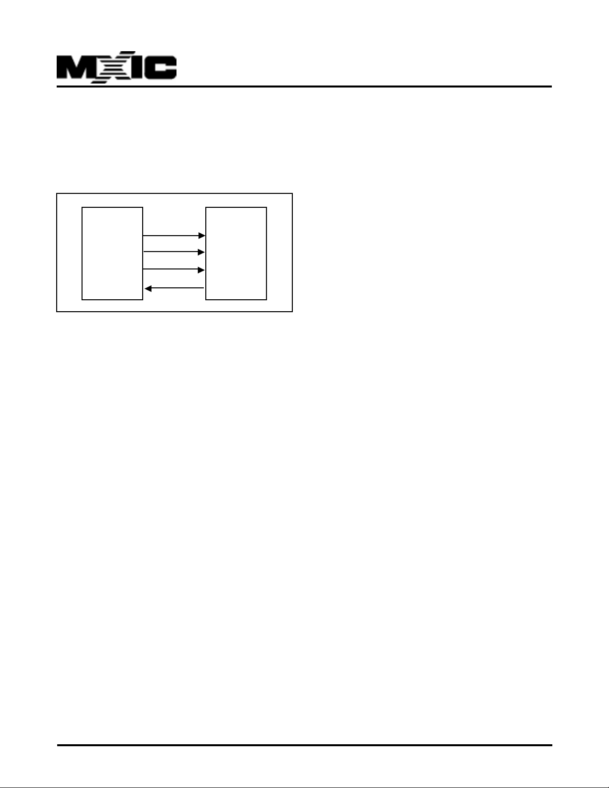
5.0 Serial ROM ( EEPROM ) Interface
Serial ROM Connection
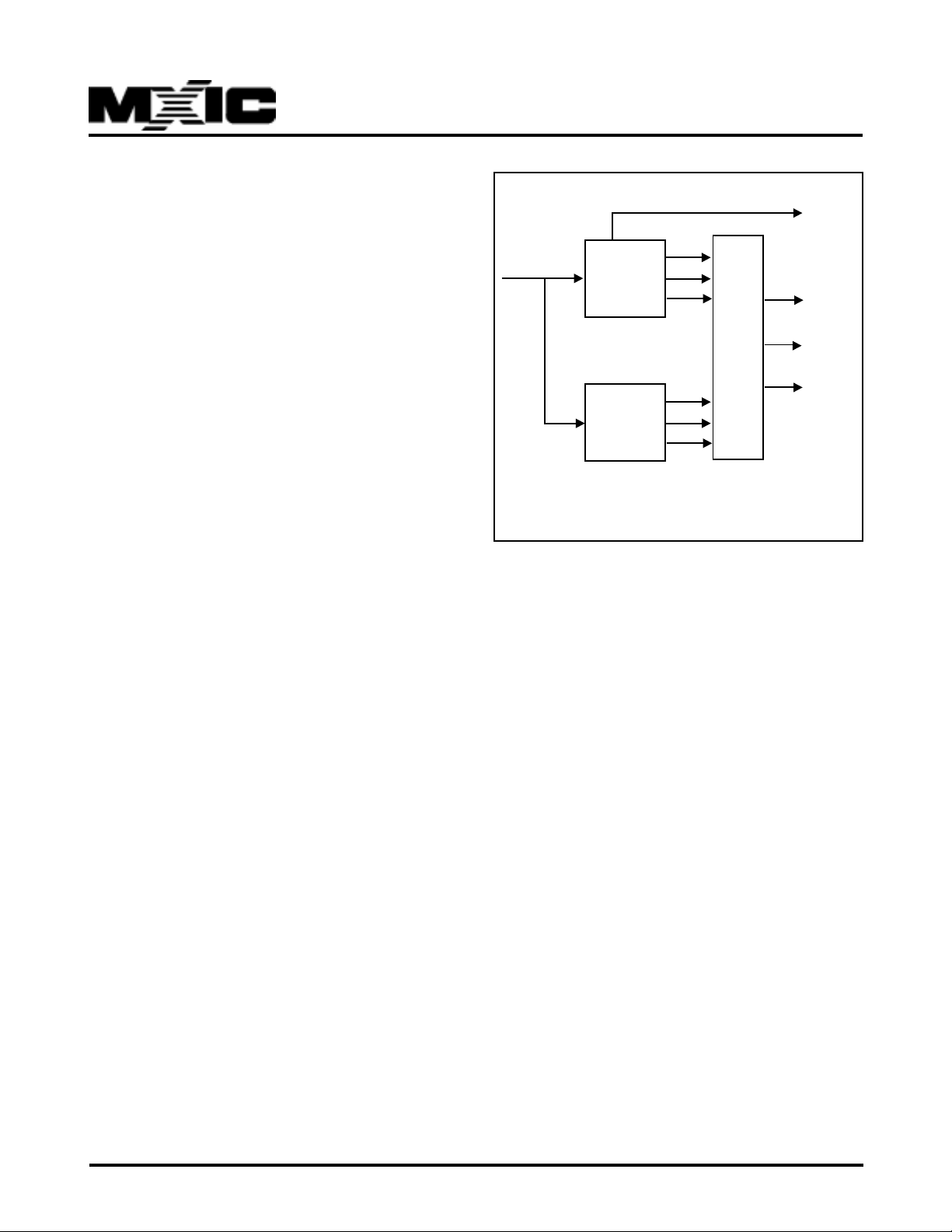
EEDO - Serial ROM (EEPROM) Data Out = Register
1Ch, bit 3
GMAC
EESC
EECK
EEDI
EEDO
EEDI - Serial ROM (EEPROM) Data In = Register1Ch,
bit2
EECK - Serial ROM (EEPROM) Serial Clock = register
1Ch, bit 1
EECS - Serial ROM (EEPROM) Chip Select = register
1Ch, bit 0
EESEL - must be set to enable the EEPROM access
by register 1Ch, bit 4
5.1 Software Programming Interface
A read operation consists of three phases :
1. Command phase - 3 bits ( binary code of "110")
2. Address phase - 6 bits for 256- to 1K-bit ROMs ( C46/
C66 pin is high), 8 bits for 2K- to 4K-bit ROMs ( C46/
C66 is forced low )
3. Data phase - 16 bits for all type of EEPROMs.
Serial ROM
(Micro Wire)
SK
CS
DIN
DOUT
These phases are generated through a sequence of writes
to 1Ch. In certain action, the driver must wait until the
minimum timing requirement for the serial ROM operation is met in order to advance to the next action.
The software sequence is available in the C source code
from MXIC.
A typical read cycle can look like this(EESEL bit is set
)
Write register 1Ch 10H ( >= 30ns )
Write register 1Ch 11H ( >= 50ns )
Write register 1Ch 13H ( >= 250ns )
Write register 1Ch 11H ( >= 100ns )
Write register 1Ch 15H ( >= 150ns )
Write register 1Ch 17H ( >= 250ns )
Write register 1Ch 15H ( >= 250ns )
Write register 1Ch 17H ( >= 250ns )
Write register 1Ch 15H ( >= 100 ns )
Write register 1Ch 11H ( >= 150 ns )
Write register 1Ch 13H ( >= 250 ns )
Write register 1Ch 11H ( >= 100ns )
Write register 1Ch 00H ( >= 150 ns )
Write register 1Ch 00H ( >= 250 ns )
Write register 1Ch 00H ( >= 100ns )
Write register 1Ch 03H ( >= 100ns )
Read register 1Ch.3 = DX ( >= 150ns )
Write register 1Ch 01H ( >= 250ns )
Write register 1Ch 00H ( >= 100ns )
END
P/N:PM0599 REV. 0.6, JUN. 22, 2000
7
Page 8
A Write operation consist of three phases :
1. Command phase - 3 bits ( binary code of "110" )
2. Address phase - 6 bits for 256- to 1K-bit ROMs, 8 bits
for 2K- to 4K-bit ROMs.
3. Data phase - 16 bits.
These phases are generated through a sequence of writes
to 1Ch. In certain action, the driver must wait until the
minimum timing requirement for the serial ROM operation is met in order to advance to the next action. A
typical driver sequence can look like this
(from eeprom)
EEDO
MX98728EC
Register 1Ch
MUX
EEDI
EECS
EECK
Write register 1Ch 00H ( >= 30ns )
Write register 1Ch 01H ( >= 50ns )
Write register 1Ch 03H ( >= 250ns )
Write register 1Ch 01H ( >= 100ns )
Write register 1Ch 05H ( >= 150ns )
Write register 1Ch 07H ( >= 250ns )
Write register 1Ch 05H ( >= 100ns )
Write register 1Ch 01H ( >= 150ns )
Write register 1Ch 03H ( >= 250 ns )
Write register 1Ch 01H ( >= 100 ns )
Write register 1Ch 05H ( >= 150 ns )
Write register 1Ch 07H ( >= 250 ns )
Write register 1Ch 05H ( >= 100ns )
Write register 1Ch 00H ( >= 150 ns )
Write register 1Ch 00H ( >= 250 ns )
Write register 1Ch 00H ( >= 100ns )
Write register 1Ch 03H ( >= 150ns )
Write register 1Ch 0XH ( >= 250ns )
Write register 1Ch 0XH ( >= 100ns )
EEDI
(to eeprom)
Auto Load
EEPROM Logic
Serial ROM Interface Block Diagram
Write register 1Ch 00H ( >= 250ns )
Write register 1Ch 01H ( >= 250ns )
*Read register 1Ch.3
if register 1Ch.3 = 1 then go on
Write register 1Ch 00H ( >= 250ns )
else
Wait 1 ms then go to *Read register 1Ch.3
END
P/N:PM0599 REV. 0.6, JUN. 22, 2000
8
Page 9

MX98728EC
5.2 Autoload Function
The Autoload Function is executed only once after the hardware reset pin RSTB from low to high. At that time the
Serial ROM interface is driven by the internal circuit to load the data of the Serial ROM.
5.3 EEPROM Content ( suggested )
Location Content
00H Physical Address Byte 0 : PAR[7:0] ( MSB )
01H Physical Address Byte 1: PAR[15:8]
02H Physical Address Byte 2 : PAR[23:16]
03H Physical Address Byte 3 : PAR[31:24]
04H Physical Address Byte 4 : PAR[39:32]
05H Physical Address Byte 5 : PAR[47:40]
06 H GMAC Configuration A Register : GCA[7:0]
bit 0 : BPSCRM
bit 1 : PBW
bit 2 : SLOWSRAM
bit 3 : ARXERRB
bit 4 : MIISEL
bit 5 : A UT OPUB
bit 6 : TXFIFOCNTEN
bit 7 : RESER VED
07H reserved
08H-END Reserved for Software application
P/N:PM0599 REV. 0.6, JUN. 22, 2000
9
Page 10
MX98728EC
6. PCB layout recommendation
Introduction:
Due to the high frequency and the increasing degree of integration, system board designs are becoming complex. The
purpose of this section is to give system designer more information. Such as pow er stability , placement, signal trace
routing and de-coupling capacitor.
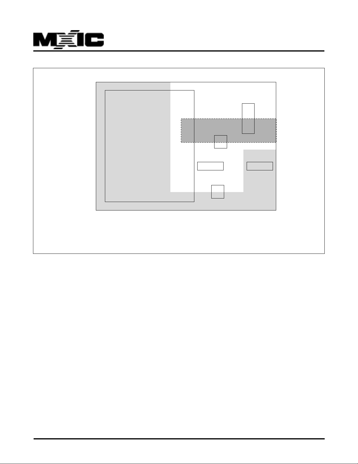
6.1 Power / Gr ound consideration
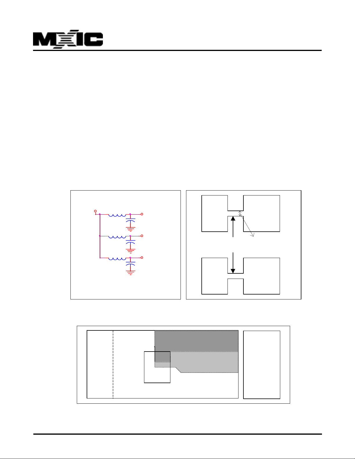
It is recommended to separate power plane into 3 domains (Power for digital , analog and receive section). Segmented power supplies reduces noise from one section to another .
It is also recommended to separate ground plane into 3 domains ( Digital Ground, Analog Ground and Receive
Ground). The reason f or separating is to prev ent digital noise from coupling onto the analog or receive ground.
All power/ground lines should be as wide as possible to allow noise de-coupling and efficient low resistive paths for
supply current.
3.3V
bead
V digital
V analog
GND GNDR
40mil
Bridge
V receive
GND GNDA
Depending upon the environment, any or all of these filters may be simplified.o
GNDR
(Receive ground)
GNDS
CardBus
GNDA
(Chassis
Interface
(Analog ground)
ground)
GND
(digital ground)
P/N:PM0599 REV. 0.6, JUN. 22, 2000
10
Page 11
6.2 Board Layout / Trace Routing
Oscillat
¨
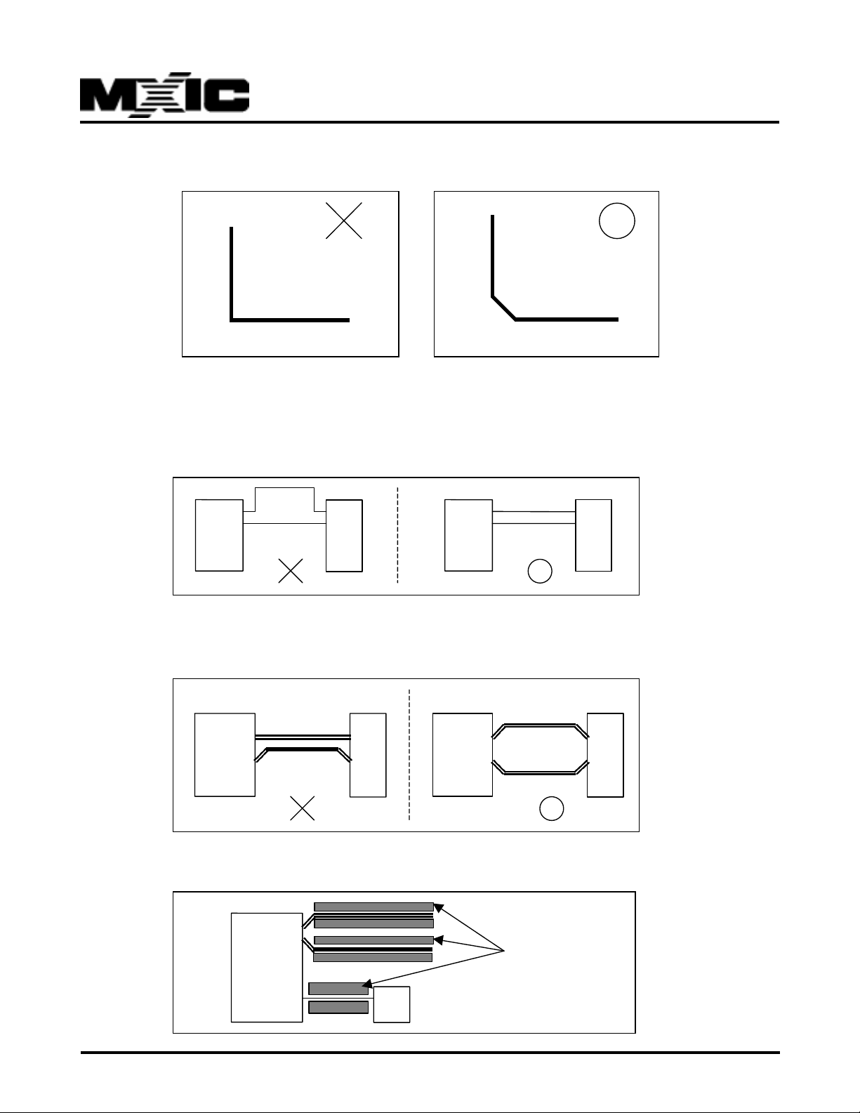
90 degree corners should be avoided, smooth cornering is preferred.
¨
Keep the lengths of clock lines short and minimize the numbers of VIAs.
¨
All pair lines ( i.e. TX+/- , RX+/-) are of the equal length and run in parallel
then possible noise is common and can be ignored on different inputs.
MX98728EC
Magnetic
Tx+
Tx-
¨
A good practice is that never run transmit and receive pair too close.
Crosstalk may become a problem.
Tx+
Tx-
Rx+
Rx-
¨
The ground shield of clock line may reduce extra noise.
Magnetic
Tx+
Tx-
Tx+
Tx-
Rx+
Rx-
Magnetic
Magnetic
Tx+
Tx-
Rx+
Rx-
Ground Shield
or
P/N:PM0599 REV. 0.6, JUN. 22, 2000
11
Page 12
MX98728EC
¨
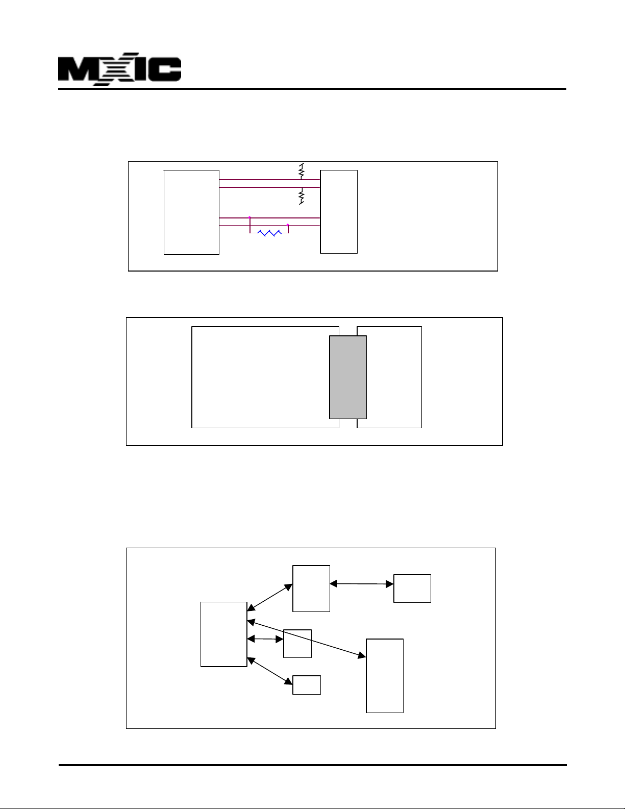
All differential pair ( Tx +/ - , Rx +/-) to the magnetic should have matched
impedance. See schematics for details.
V
50
Tx+
Tx-
V
Rx+
Rx-
100 Ohm
¨
A chassis ground is used to isolate the cable side and ground.
Magnetic
50
Magnetic
Chassis
System Ground
6.3 Component placement
General:
External components are placed as close as possible
Magnetic
Osc/Crystal
IC
Ground
RJ-45
BootROM
EEPROM
P/N:PM0599 REV. 0.6, JUN. 22, 2000
12
Page 13
MX98728EC
¨
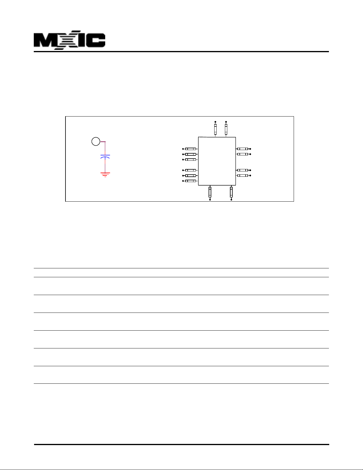
De-coupling capacitor
De-coupling cap should be placed close to power pin. It stabilize current to
the device and de-coupling noise from the power plane to ground.
PIN
0.1 U
IC
¨
VDD/GND Pins
PIN# Pin Name Description
51,54,59,70,78,81,83 VDD A Analog Vdd Pins : Must be carefully isolated in the separ ated
Vdd plane.
52,57,58,73,74,79,80, GNDA Analog Ground Pins : Must be carefully isolated in the sepa82,84 rated GND plane.
62,63,66,67 VDDR RX Vdd Pins : Must be carefully isolated in the separated Vdd
plane.
60,61,68,69 GNDR RX Ground Pins : Must be carefully isolated in the separated
ground plane.
42,30,2,153,115,107 VDD Digital Vdd Pins : Must be carefully isolated in the separated
15 8 Vdd plane.
41,39,34,22,7,154, GN D Digital Ground Pins : Must be carefully isolated in the separated
146,121,116,104,98, 85, 86 ground plane.
P/N:PM0599 REV. 0.6, JUN. 22, 2000
13
Page 14
MX98728EC
MX98728EC
85
84
VDDR
GNDR
Receive Region
Analog Region
TX+
TXRX+
RX-
Bead
Digital Region
1
GNDA
VDDA
VDD
XTAL 25MHz
Analog Region
Bead
POWER PLANE OF PCB LAYOUT
OSC 25MHz
Digital Region
P/N:PM0599 REV. 0.6, JUN. 22, 2000
14
Page 15
MX98728EC
10K
RDA
R1
+5V
LED0
1.4K
+5V
LED1
RXIP
RXIN
MX98728EC
TXOP
RTX2EQ
R2
560
TXON
RTX
R3
APPLICATION CIRCUIT
R5
R4
100
+5V
+5V
50
50
R6
1:1
ST6118
RJ45
HOST
GND
HOST
VDD
Note: If EMI issue @ 125MHz, 250MHz, 375MHz, TXOP, TXON
can each connects a 22pf capacitor to ground.
CHASSIS GND
RJ45
Digital
GND
Digital
VDD
Bridge
Analog GND
F.B.
Analog VDD
TX
TX
TX
Transformer
Bridge
F.B.
RX
narrow PCB trace
RX
Analog GND
RX
Analog VDD
PCB POWER PLANE
P/N:PM0599 REV. 0.6, JUN. 22, 2000
15
Page 16
MX98728EC
APPENDIX A: SPECIAL COMPONENTS
1.MAGNETIC
A.BASIC ELECTRICAL SPECIFICA TION
T urn Ratio T ransmit 1:1
Receive 1:1
OC L 350uH min measured between 0 and 70°C with a 0.1V rms, 100KHz
signal at a DC. bias between 0 and 8mA.
L L 0.4uH Max at >1MHz
Cw w 18pF Max
DC R 0.9W Max per winding
Isolation Resistance not less than 1GW @ 2000V rms
Isolation Voltage 2000V rms Min @ 60Hz for 1 min
Rise/Fall Time 3ns Min 4ns Max
Insertion Loss (100 KHz to 100 MHz) -1.1 dB Max
CMDR & DCMR (100 KHz to 80 MHz) 38 dB Min
Cross Talk (100KHz to 80 MHz) -38 dB Max
B. T ransformer REFERENCE VENDORS
V endor Part No
V alor ST6118 (PT4171S)
PE PE68515
BelFuse S558-5999-15
Delta LF8200
T aimic HSIP-002
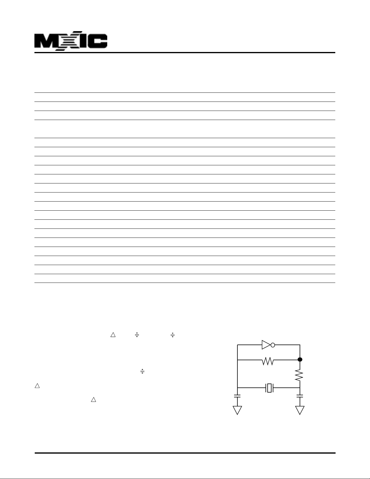
2.CRYSTAL
a.
BASIC ELECTRICAL SPECIFICA TION
CL=((C1*C2)/(C1+C2))+CIC+ C, Rd 100 ohm,R 1M ohm
CL=Crystal's external load capacitor
Specified by crystal's specification
CIC=MX98715AEC-E internal capacitor, 7pF
C=PCB's stray capacitance
Assume C1=C2=C
CL=1/2C
+ 7pf + 3pf
Ext
if CL=20pf, than C
P/N:PM0599 REV. 0.6, JUN. 22, 2000
, C=3pf,
Ext
Ext=C1=C2
=20pf.
16
C1
IC
R
Rd
C2
Page 17

MX98728EC
b. CR YST AL REFERENCE VEDORS
SPK 25MHz±50PPM
NDK...
JEN JAAN ENTERPRISE
3. SPECIAL REQUIREMENT ON RESIST ORS & BEAD
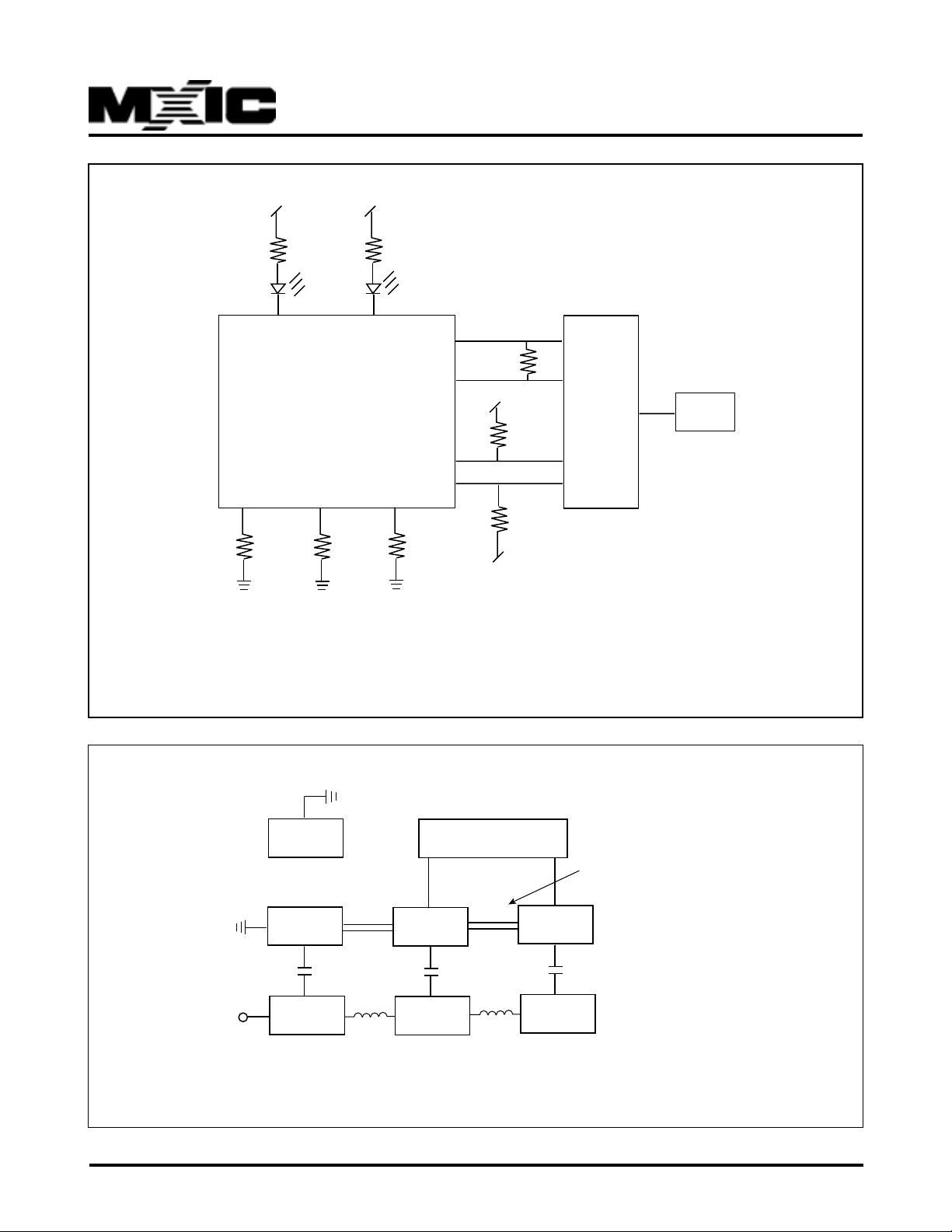
Resistors for RTX=560 ohm ± 1%
Resistor for RTX2EQ=1.4K ± 1%
Resistor for RD A=10K ± 5%(F or 10 Base-T Vpp swing)
Ferrite Bead maximum current capacity for analog Vdd > 300mA
Ferrite Bead maximum current capacity for Receiv e Region Vdd > 100mA
4. Board Current Measurement
Sepearted Power Plane Current 100 Base-TX Mode 10 Base-T mode
Total board current <= 190 ma <= 230 ma
T otal Analog current <= 140 ma <=190 ma
Total RX current <= 60 ma <= 85 ma
Appendix B: Cable Brands used in Driver tests
Brand :
AMP (systems cable E138034 02-L 24 A WG (UL) CMR/MRP C(UL) PCC FT4 verified CA T5 9640)
Length: 60m,100m
Brand :
A T&T-Q ( SYSTEMAX 1061C 4/24 CM v erified (UL) or C(UL) CUH JJ03076
Length : 100m, 120m, 1m
Brand : BDN
Length : 60m, 80m, 130m
Brand : Belden-M (Data Twist ( R ) Five 1583A CM 4PR24 v erified (UL) CA T5 E108998 or C(UL) CM 1108
Length : 100m
Brand : CTI ( ETI v erified to EIA/TIA 568 CAT 5 UTP-4 pairs 24AWG UT5004)
Length : 100m
Brand : Lucent-C ( systemax 1061c+ 4/24 CM verified (UL) CA T5 E1035946
Length : 10m, 20m, 60m, 80m, 100m
Brand : Planet CAT 5 100Mbps 4PR24 STP solid cable
Length : 10m
P/N:PM0599 REV. 0.6, JUN. 22, 2000
17
Page 18
Appendix C: IEEE802.3 CONFORMANCE TEST
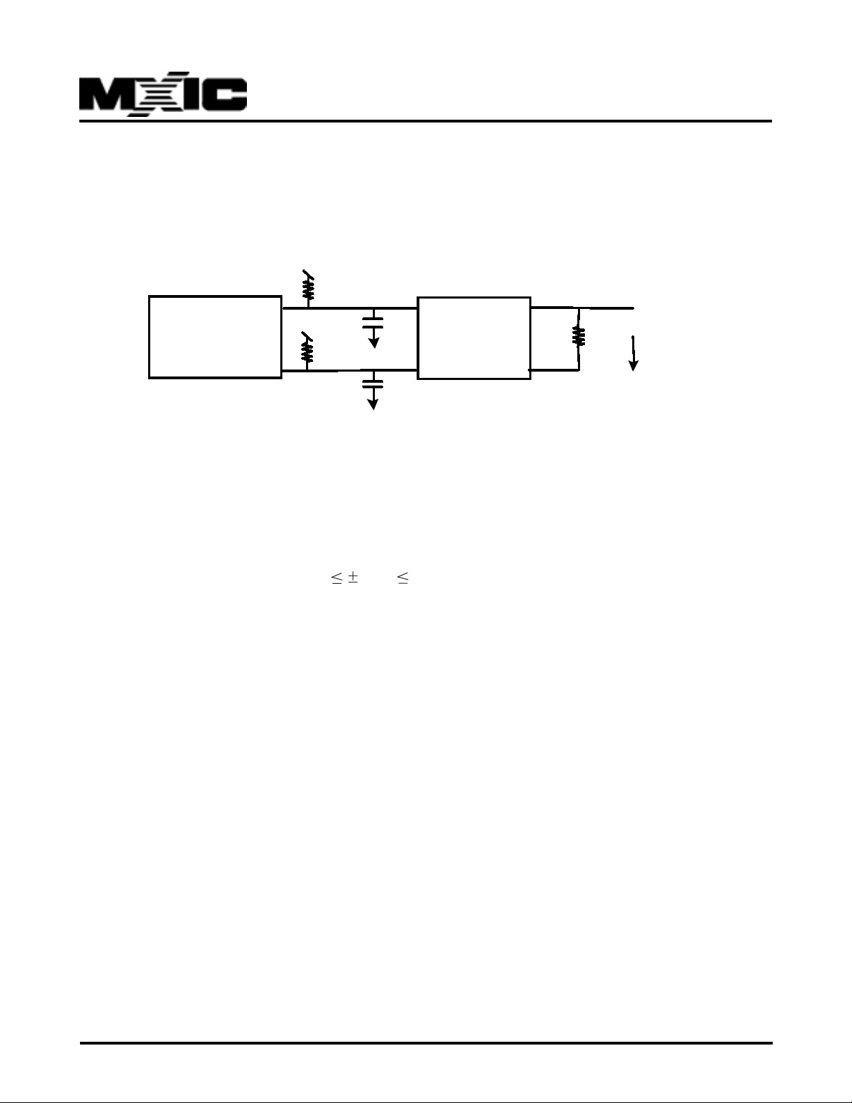
1. Testing Conditions
(1) DUT diagram (using MX98715 standard 2-layer PCB demo board)
5V
MX98728EC
TXOP
50
5V
33 pF
Transformer
MX98728
TXON
50
(2) Testing equipment and setting
T ektronix TDS744A Digitizing Oscilloscope
trigger Slope +
rise time: 10% ~ 90%
fall time: 90% ~ 10%
probe input capacitance: 1pF
probe input impedance: 200K ohm
2. UTP Differential Output Test (950mV Vout 1050mV)
(1) Vout (+) = 500.0mV
(2) Vout (-) = -500.0mV
(3) Result: Pass
3. UTP Active Output Interface T emplate T est
(1) UTP active output interface template
(see below scanned figure)
33 pF
1:1
10 0
+
V
out
_
P/N:PM0599 REV. 0.6, JUN. 22, 2000
18
Page 19
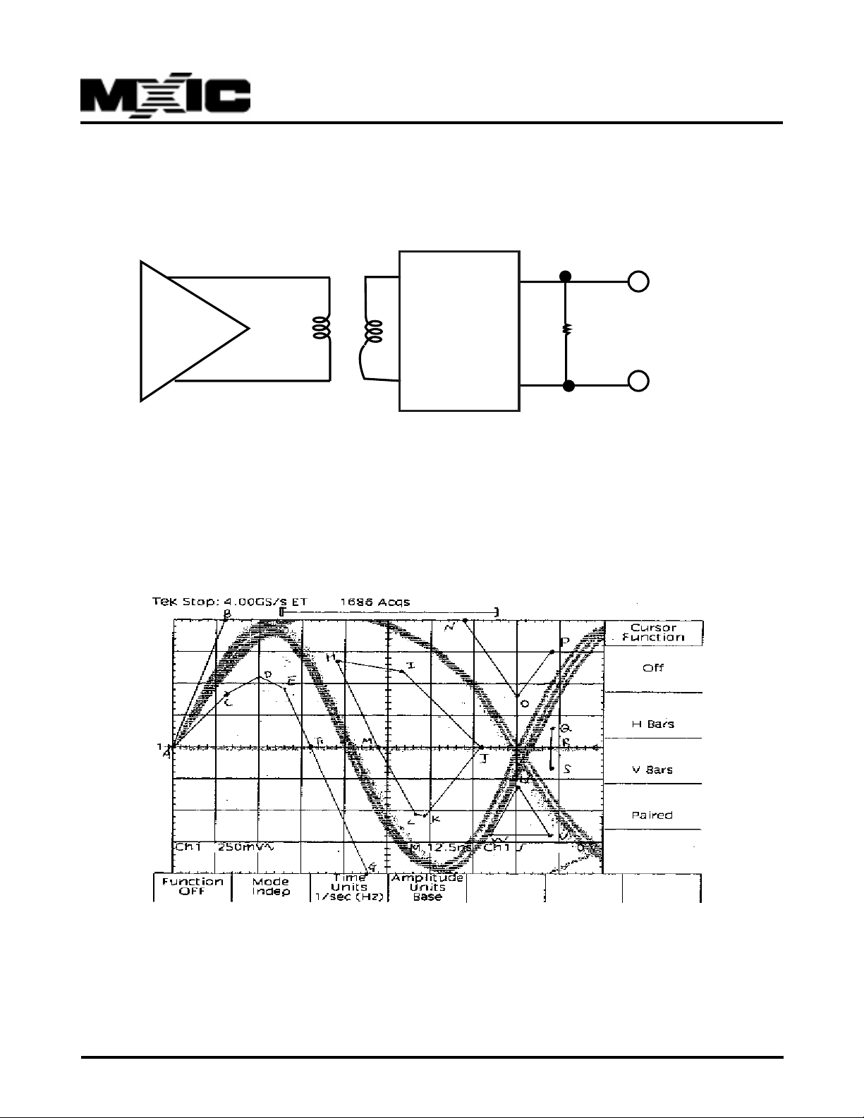
3 UTP Active Output Interface Templace Test
(1) 10 BT Transmit tenplate checker
TXOP
+
_
TXON
TP -
Model
MX98728EC
+
100
_
V0
(2) UTP active output interface template
10 BT Transmit Templatc
P/N:PM0599 REV. 0.6, JUN. 22, 2000
19
Page 20
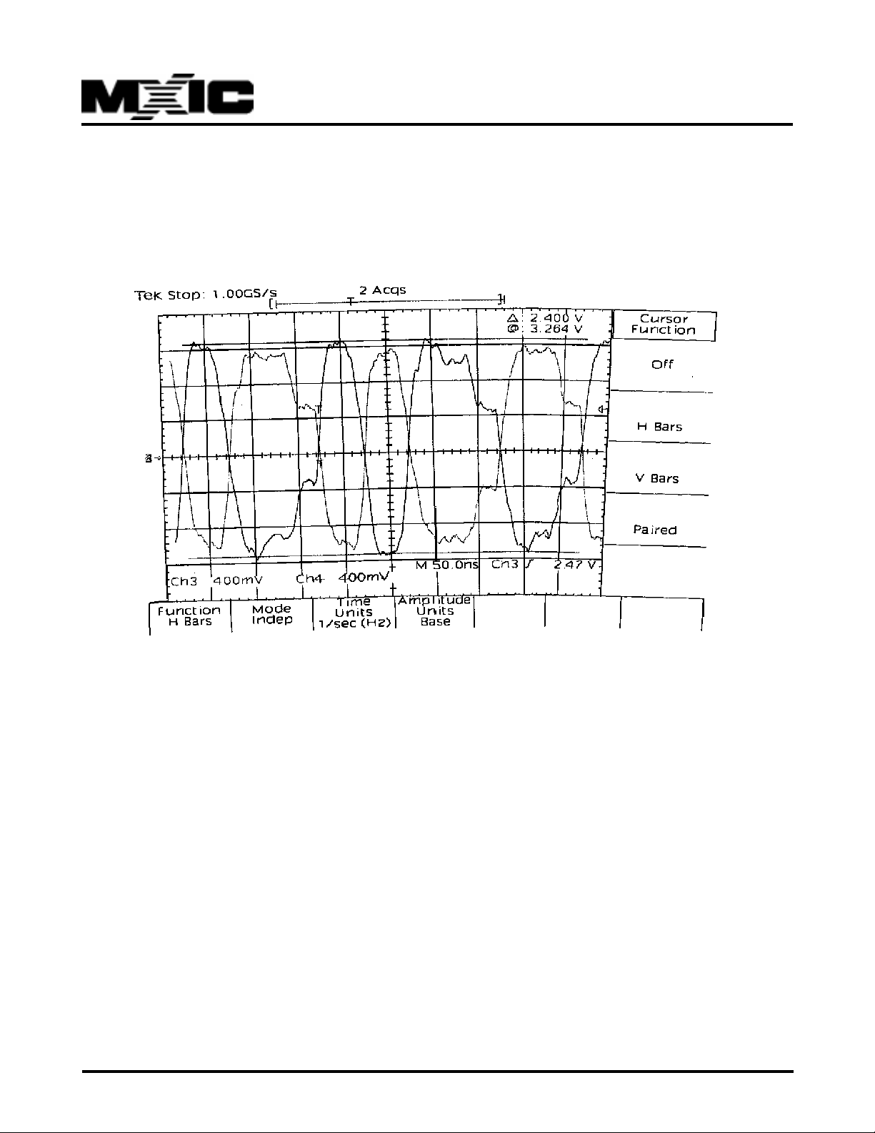
(3) 10BT Transmit waveform
MX98728EC
Result: Pass
P/N:PM0599 REV. 0.6, JUN. 22, 2000
20
Page 21
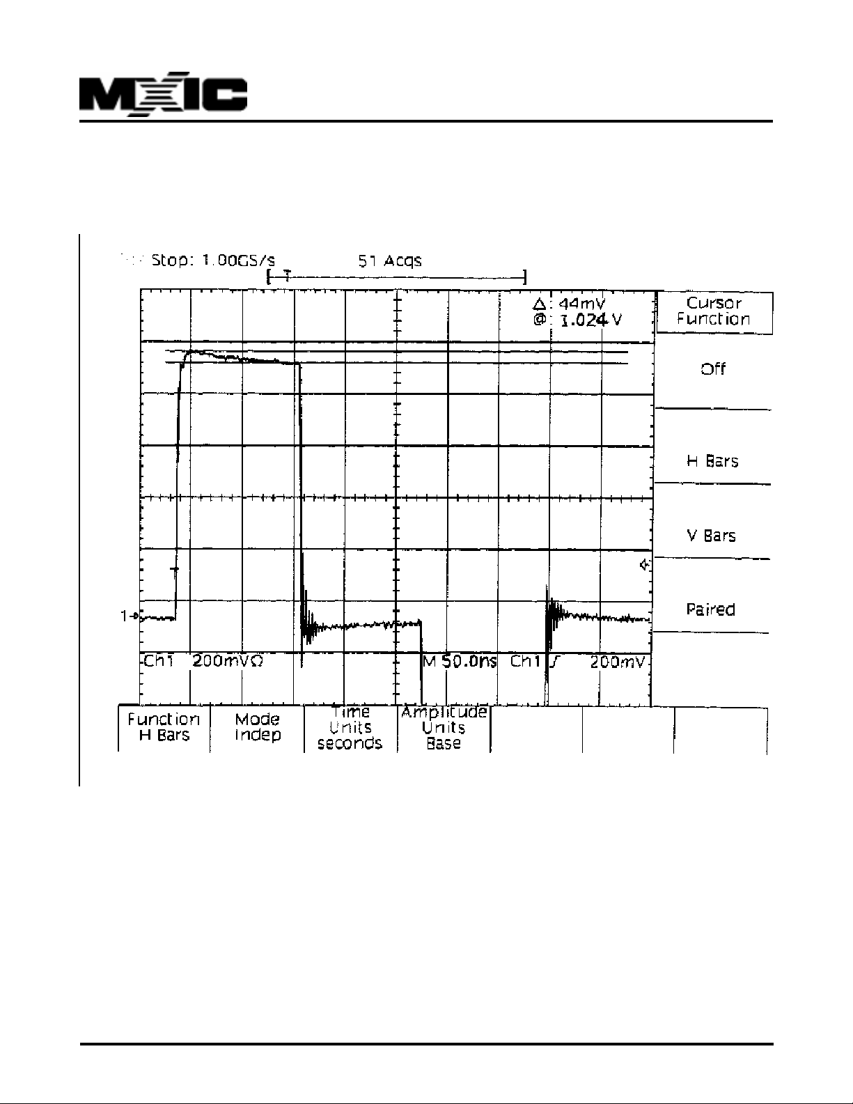
4. Vout T ransmit W aveform Overshoot (shall not e xceed 5%)
(1) V out (+) pattern
(see below scanned figure)
MX98728EC
100BT Transmit overshoot non-scramble pattern=000000000000001- - - - -
P/N:PM0599 REV. 0.6, JUN. 22, 2000
21
Page 22
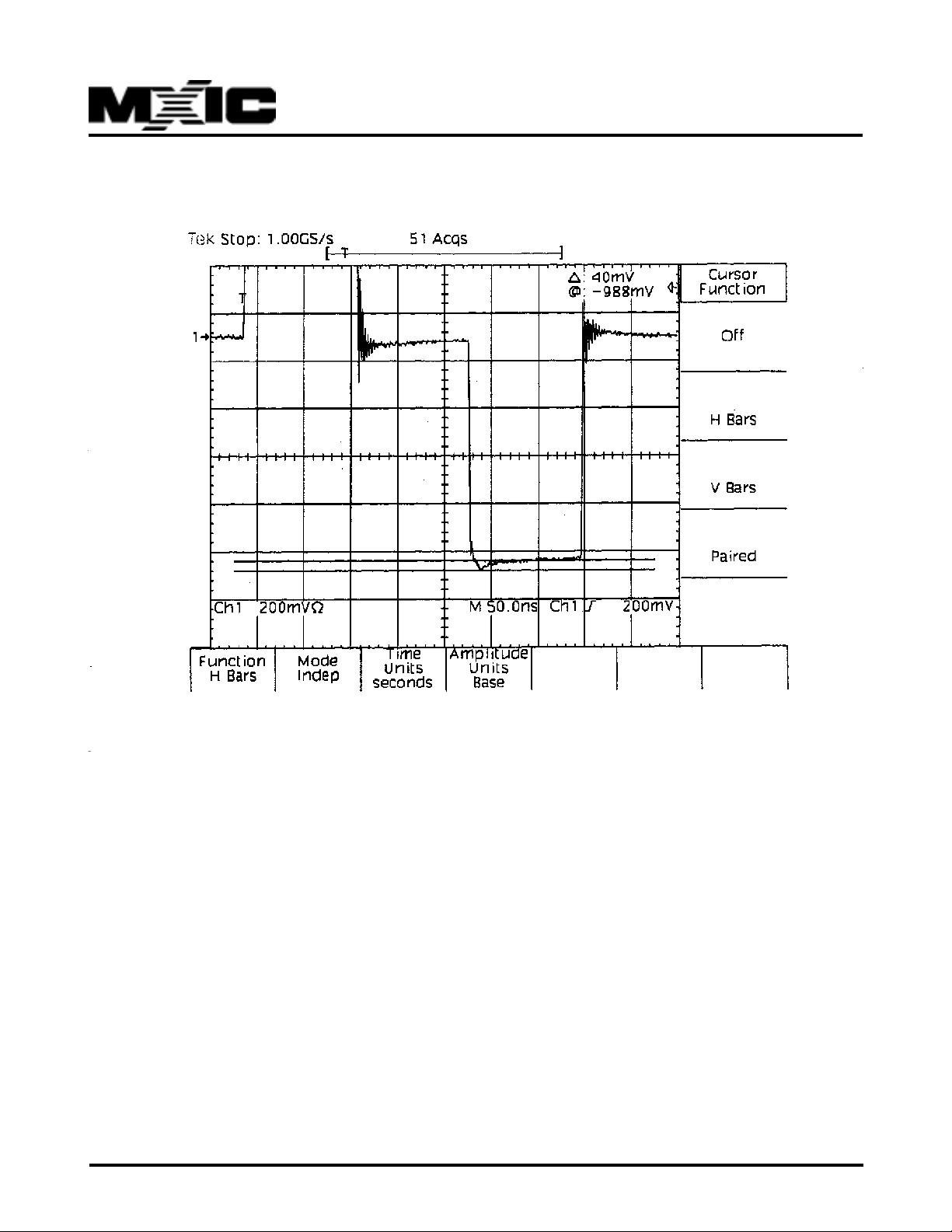
(2) V out (-) pattern
(see below scanned figure)
MX98728EC
100BT Transmit overshoot non-scramble pattern=000000000000001- - - - -
(3) Result: Pass
P/N:PM0599 REV. 0.6, JUN. 22, 2000
22
Page 23
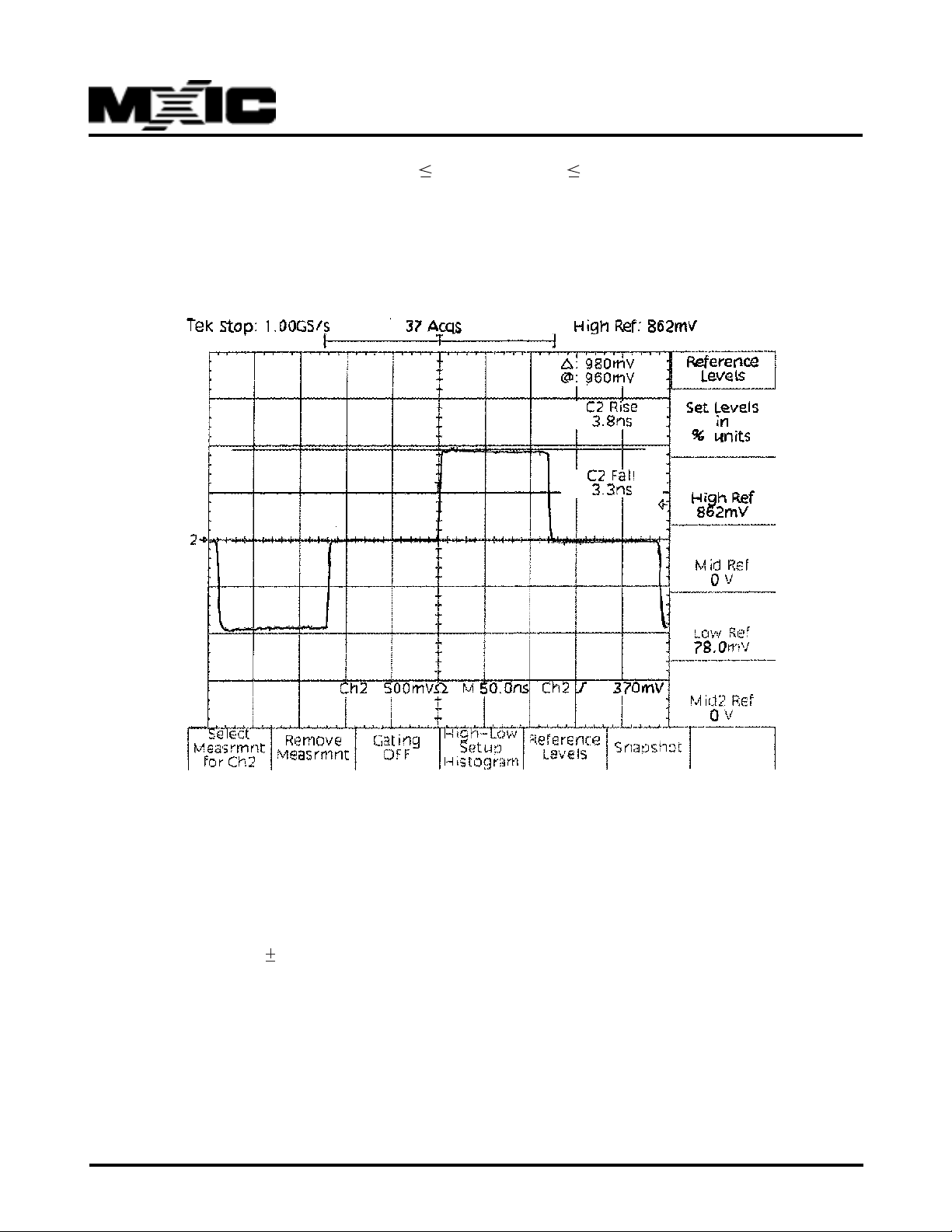
5. T ransmit Signal Amplitude Symmetry (0.98 +V out(+) / -Vout(-) 1.02)
(1) Vout(+) = 500mV
(2) V out(-) = -500mV
(3) Results: P ass
6. V out T ransmit Rise/F all Times (3.0nsec < T rise/fall < 5.0nsec)
MX98728EC
100BT Transmit rise/fall time . non-scramb le pattern=000000000000001 - - - - -
(3) Results: Pass
7. Vout T ransmit Duty Cycle Distortion (The de viation of the 50% crossing times from a best fit to a time grid
of 16ns shall not exceed .25ns) (DSO: Lecro y9384, Vcc: 5.0V olts)
(1) Amplitude Results
(see below scanned figure)
P/N:PM0599 REV. 0.6, JUN. 22, 2000
23
Page 24
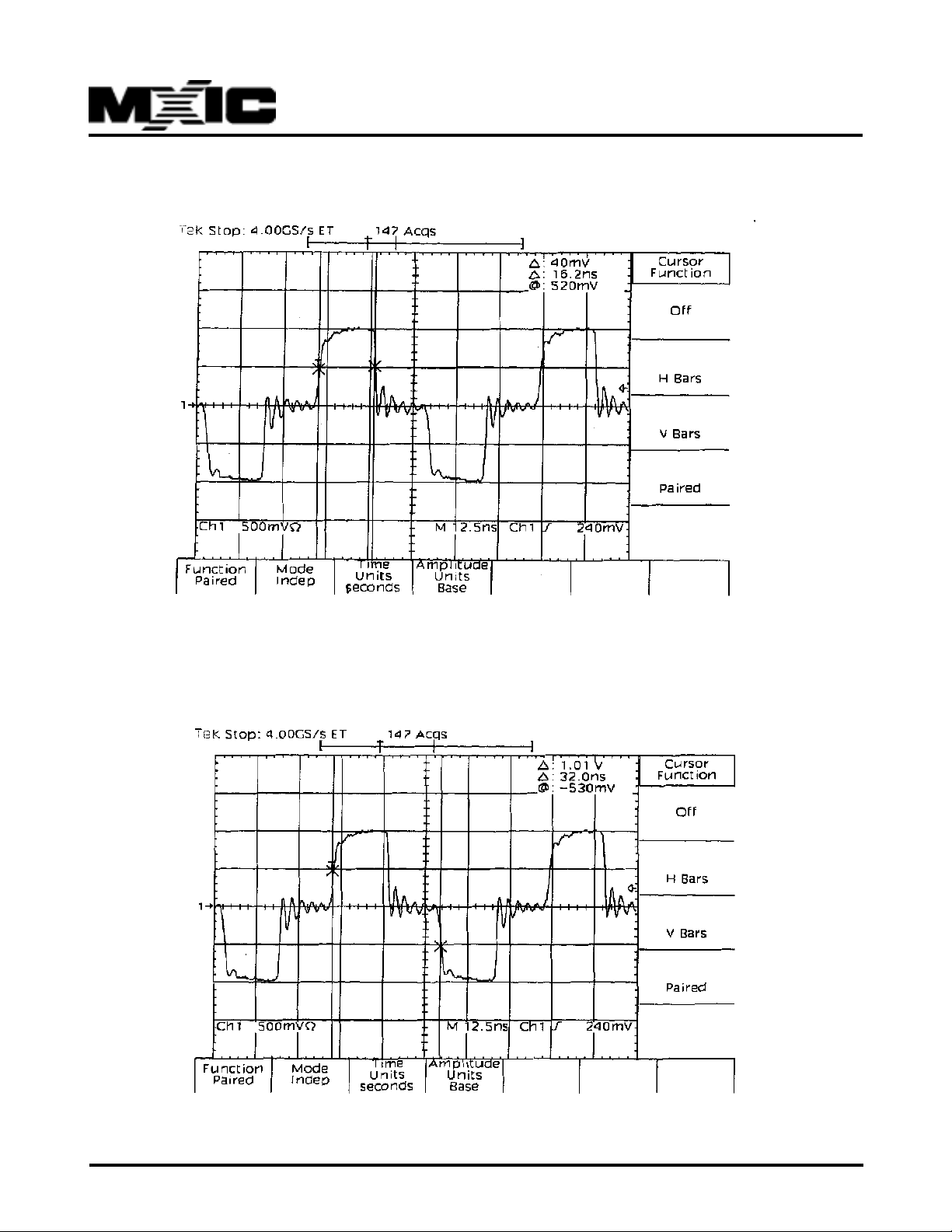
(2) First half cycle
(see below scanned figure)
MX98728EC
100BT Transmit Duty Cycle Distortion. non-scramble pattern=010101 - - - - -
(3) Second half cycle
(see below scanned figure)
100BT Transmit Duty Cycle Distortion. non-scramble pattern=010101 - - - - -
P/N:PM0599 REV. 0.6, JUN. 22, 2000
24
Page 25
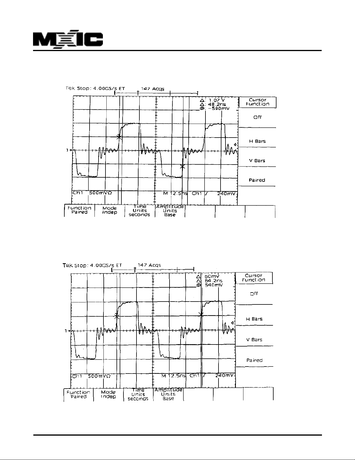
(4) Third half cycle
(see below scanned figure)
MX98728EC
100BT Transmit Duty Cycle Distortion. non-scramble pattern=010101 - - - - -
(5) Fourth half cycle
(see below scanned figure)
100BT Transmit Duty Cycle Distortion. non-scramble pattern=010101 - - - - -
(6) Test Result : P ass
P/N:PM0599 REV. 0.6, JUN. 22, 2000
25
Page 26
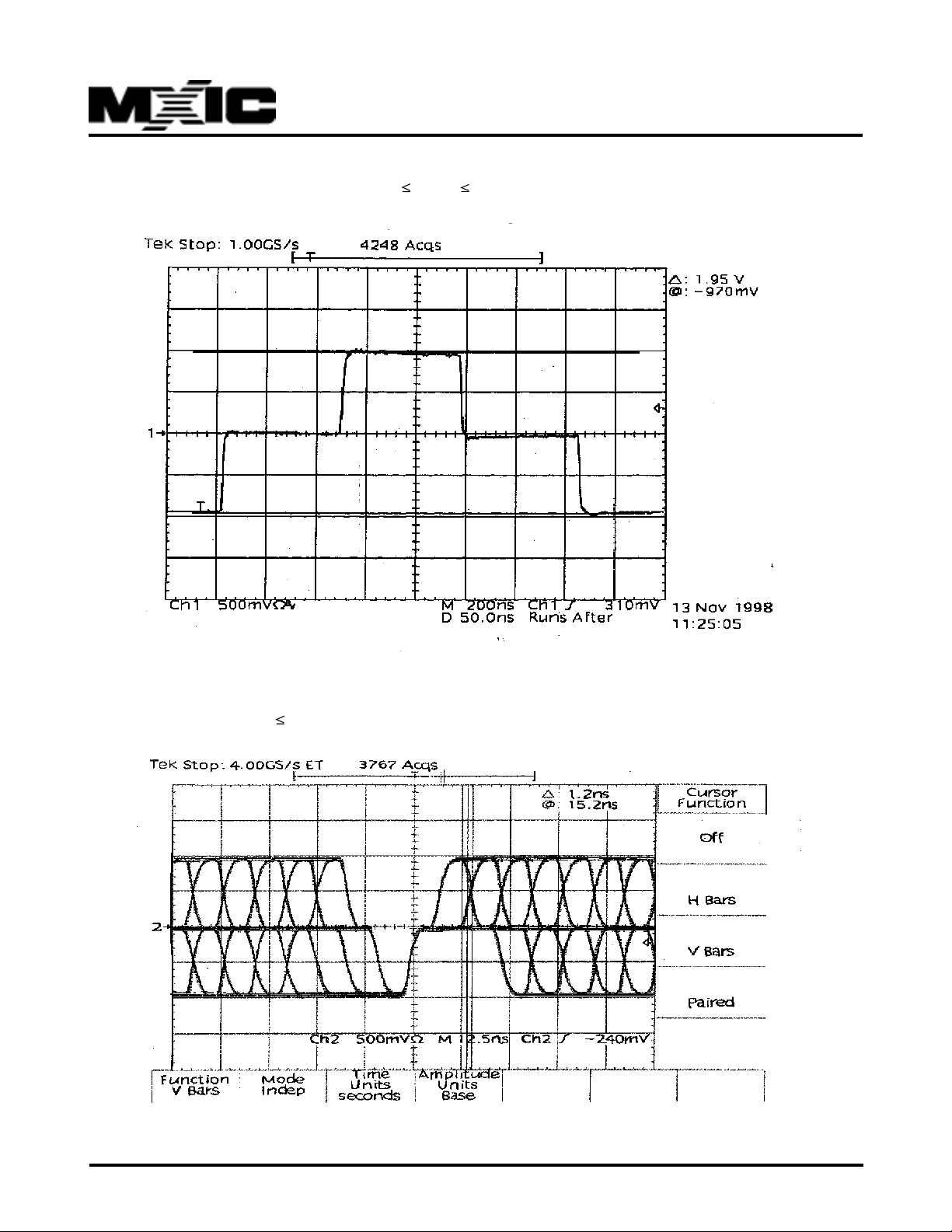
8. Transmit peak to peak votlage (1.9V Vpp 2.1V)
MX98728EC
100BT Transmit Vpp non-scramble pattern=000000000000001 - - - - -
9. Transmit jitter ( jitter 1.4ns)
100BT Transmit jitter random pattern
P/N:PM0599 REV. 0.6, JUN. 22, 2000
26
Page 27

MX98728EC
REVISION HISTORY
Revision No. Description P age Date
0.3 Rearrange loopback mode descriptions P5 JUN/21/1999
Add MX98728EC, MX98728AEC description P1
0.4 Fig3 application circuit 12K-->10K P11 NO V/23/1999
Add appendixA&B P12~20
0.5 Add appendix C P14~22 DEC/02/1999
0.6 Modify introduction and product overview P1 JUN/22/2000
Add combo application and typical application P2~3
Add 3.8 MII interface P4
Modify 4.8 Receive buffer ring full P5
Modify EEPROM content (06H) P9
Modify PCB Layout recommendations P10~14
P/N:PM0599 REV. 0.6, JUN. 22, 2000
27
Page 28

TOP SIDE MARKING
MX98728EC
MX98728EC
C9930
TA777001
38BAX
TAIWAN
MACRONIX INTERNA TIONAL CO., LTD.
HEADQUARTERS:
TEL:+886-3-578-6688
FAX:+886-3-563-2888
line 1 : MX98728 is MXIC parts No.
"E" :PQFP
"C" : commercial grade
line 2 : Assembly Date Code.
line 3 : Wafer Lot No.
line 4 : "38B" : revision code,
"A" : bonding option
"X" : no used
line 5 : State
EUROPE OFFICE:
TEL:+32-2-456-8020
FAX:+32-2-456-8021
JAPAN OFFICE:
TEL:+81-44-246-9100
FAX:+81-44-246-9105
SINGAPORE OFFICE:
TEL:+65-348-8385
FAX:+65-348-8096
TAIPEI OFFICE:
TEL:+886-2-2509-3300
FAX:+886-2-2509-2200
MACRONIX AMERICA, INC.
TEL:+1-408-453-8088
FAX:+1-408-453-8488
CHICAGO OFFICE:
TEL:+1-847-963-1900
FAX:+1-847-963-1909
http : //www.macronix.com
MACRONIX INTERNATIONAL CO., LTD. reserves the right to change product and specifications without notice.
 Loading...