

Page 1
1. INTRODUCTION
PRELIMINARY
MX98715BEC
APPLICATION NOTE
The purpose of this application note is to describe the
implementation of a PCI bus master 100 Base-TX F ast
Ethernet node using MXIC’ highly integrated single chip
Fast Ethernet NIC controller MX98715BEC. In details,
this document presents product overview , programming
guide, hardware design and layout recommendations that
can help you to quickly and smoothly implement a F ast
Ethernet adapter card.
As you can find in the MX98715BEC driver diskette,
MXIC already provideds a complete set of high quality
drivers for easier and more efficient way to interface with
MX98715BEC on the most popular Network Operating
Systems. Nev ertheless, there are still some special applications or environment not covered in the
MX98715BEC driver diskette. Driver developers, however, could still refer to the section of driver programming guide to accomplish the required driver. It is recommended that you should be familiar with the
MX98715BEC data sheet before reading this guide.
2. PRODUCT OVERVIEW
The MX98715BEC implements the 10/100Mbps MAC
layer and Physical layer on a single chip in accordance
with the IEEE 802.3 standard.
The MX98715BEC highly integrates with direct PCI bus
interface, including PCI bus master with DMA channel
capability, direct EEPROM as well as Boot ROM interface, and large on chip transmit/receive FIFOs. Also,
the MX98715BEC is equipped with intelligent
IEEE802.3u-compliant Nway auto-negotiation capability
allowing a single RJ-45 connector to link with the other
IEEE802.3u-compliant device without re-configuration.
T o optimiz e operating bandwidth, network data integrity
and throughput, the proprietary Adaptive Network
Throughput Control (ANTC) function is implemented. For
detailed product specification information, please refer
to the MX98715BEC data sheet.
3. HARDWARE DESIGN CONSIDERATIONS
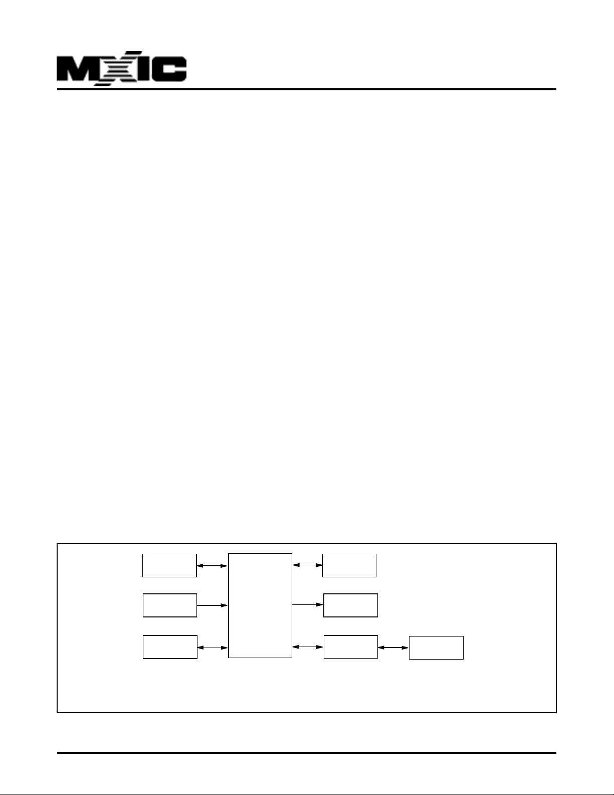
3.1 SYSTEM APPLICA TION BLOCK DIAGRAM
A system block diagram for the MX98715BEC based
Fast Ethernet adapter card is shown as f ollowing:
P/N:PM0706
PCI Bus
Osc or Crystal
25MHz
EEPROM
MX98715BEC
Fig. 1
Boot ROM
LED
Magnetic
1
RJ45
REV. 0.2, NOV. 30, 2000
Page 2

3.2 PCI CONNECTION
The MX98715BEC provides direct PCI bus interface to
PCI connector. Board designers should especially take
care of the four pins of TDI,TDO,PRSNT1# & PRSNT2#
that are only related to PCI bus connector . Boards that
do not implement JT A G Boundary Scan should tight TDI
and TDO together to pre vent the scan chain from being
broken.
Both pins PRSNT1# and PRSNT2# should be connected to ground indicating that the board physically
exists in a PCI slot and provids information about the
total power requirements ( less than 7.5W ) of the board.
3.3 OSCILLA TOR OR CR YST AL
The MX98715BEC is designed to operate with a 25MHz
oscillator or crystal module. The clock specification of
this oscillator should meet 25MHz +/- 50PPM.
MX98715BEC
CSR 9 <28> 0 1
LED 0 Activity Link speed
CSR 9<29> 0 1
LED 1 Good Link Link Activity
CSR 9<30> 0 1
LED 2 Link Speed Colision
CSR 9<31> 0 1
LED 3 Receive F/H duplex
CSR 9<24> 0 1
LED 4 Colision PMEB
3.4 BOOT R OM
The MX98715BEC support a direct boot ROM interface
allowing diskless workstations to remotely download operating system from network server. F or proper oper ation, the access time of adapt EPROM should not exceed 240ns.
3.5 SERIAL EEPROM
The MX98715BEC provides pins EECS,BPA0 (EECK),
BPA1 (EEDI) and BPD0 (EEDO) for directly accessing
the serial EEPROM. BPA0-1 and BPD0 ser ve as SK
(EECK), DI (EEDI) and DO (EEDO) respectively. The
contents of the EEPROM includes the ID information of
the MX98715BEC (V endorID , DeviceID , Sub-vendorID ,
Sub-deviceID and MAC ID), and the configuration parameters for software driver. The EEPROM contents
should be programmed according to MXIC's definition
as mentioned in Appendix A. Detailed software programming example is described in section 4.5.
3.6 PROGRAMMABLE LED SUPPORT
The MX98715BEC provides five pins LED[0:4] to control display LEDs. Displayed messages are programmable through setting CSR9 bits[31:28] & bit24. The maximum sinking current of these output pins is 16mA. Current limiting resistor (560 ohm) should be added to ensure proper operation. The following indicates the configuration setting table for LED display programming.
3.7 NETWORK INTERFACE TO MAGNETIC
COMPONENT
For isolating and impedance matching purpose, an isolating transformer with 1:1 transmit and 1:1 receive turns
ratio is required for transmit and receive twisted pair
interface. In Appendix B, several transformers that we
had verified successfully with MX98715BEC are listed
for quick reference purpose.
3.8 OPTIMIZED EQUALIZER COMPONENTS
M XI C ’ Fast Ethernet solution utilizes adaptive equalizer to compensate the attenuation and phase distortion induced by different lengths of cable. To optimize
transmit and receive signal quality, pins RTX should be
connected to external resistors 1K ohm (±1%) and then
to ground respectively.
3.9 Remote-Power -On and ACPI application
MX98715BEC fully supports Remote-Power-ON and
ACPI spec that meet PC99 requirement for powersensitive applications. It accepts the following wake-up
events in the power-down mode.
* Reception of a Magic Pack et.
* Reception of a Network wake-up frame.
* Detection of change in the network link state.
To put MX98715BEC into the sleep mode and enable
the wake-up events detection are done as following:
P/N:PM0706 REV. 0.2, NOV. 30, 2000
2
Page 3

1. Write 1 to PPMCSR [8] to enable power management
feature.
MX98715BEC
(struct TX_RESOURCE *)((((unsigned int)tx_temp[i])+4)&
0xfffc);
}
2. Write the value to PPMCSR [1:0] to determine which
power state to enter .
If D1, D2 or D3
state is set, the PC is still turned on
hot
and is commonly called entering the Remote W ak e-up
mode. Otherwise if the main power on a PC is totally
shut off, we call that it is in the D3
state or Remote
cold
Po wer-On mode. T o sustain the oper ation of the Lancard,
a 5V standby power is required. Once the PC is turned
on, MX98715BEC loads the magic ID from EEPROM
and sets it up automatically . No register is needed to be
programmed. After then, simply turn off PC to enter D3
cold
state. In either Remote W ake-up mode or Remote P owerOn mode, the transceiver and the RX block are still alive
to monitor the network activity . If one of the three wak eup events occured, the following status is changed:
1. PPMCSR [15] (PME status) is set to 1.
2. CRS5 [28] (WKUPI) is set to 1.
3. PCI interrupt pin INTA# is asserted low .
4. LANWAKE pin is asserted high.
4. DRIVER PROGRAMMING GUIDE
This chapter will provide you the necessary information
for programming driver for the MX98715BEC based node.
Initialization module is introduced first that describes how
MX98715BEC is initialized before any other operations
can commence, then followed by actual implementation
examples for both transmit and receive operations.
4.1 INITIALIZA TION
initializeTheTransmitRing()
{
unsigned int i,j;
unsigned long physicaladdress;
for (i=0; i<NumTXBuffers; i++) {
/* memory allocation for tx descriptor_buffer (align 4) */
tx_resource[i]=
for (i=0; i<NumTXBuffers; i++) {
/* initialize the own bit to host tdes0 */
tx_resource[i]->ownership=0x00;
tx_resource[i]->tstatus=0x0000;
tx_resource[i]->tdes0_unused=0x00;
/* fill buffer_1_address tdes2 */
get_ea((void far *)(tx_resource[i]->tx_buffer_data),
&physicaladdress);
tx_resource[i]->buff_1_addr=physicaladdress;
/* fill buffer_2_address tdes3 */
if (i==NumTXBuffers-1) j=0;
else j=i+1;
get_ea((void far *)(tx_resource[j], &physicaladdress);
tx_resource[i]->buff_2_addr=physicaladdress;
}
}
initializeTheReceiveRing()
{
unsigned int i,j;
unsigned long physicaladdress;
for (i=0; i<NumRXBuffers; i++) {
/* memory allocation for rx descriptor_buffer (allign 4) */
rx_resource[i]=
(struct RX_RESOURCE *)((((unsigned int)rx_temp[i])+4)&
0xfffc);
}
for (i=0; i<NumRXBuffers; i++) {
/* set the own bit to chip rdes0 */
rx_resource[i]->frame_length=RDES0_OWN_BIT;
rx_resource[i]->rstatus=0x0000;
/* fill rdes1 */
rx_resource[i]->command=RDES1_BUFFRX_BUFFER_SIZE+rxpkt_size[i];
/* fill buffer_1_address rdes2 */
get_ea((void far *)(rx_resource[i]->rx_buffer_data),
&physicaladdress);
rx_resource[i]->buff_1_addr=physicaladdress;
/* fill buffer_2_address rdes3 */
if (i==NumRXBuffers-1) j=0;
else j=i+1;
get_ea((void far *)(rx_resource[j], &physicaladdress);
P/N:PM0706 REV. 0.2, NOV. 30, 2000
3
Page 4

MX98715BEC
rx_resource[i]->buff_2_addr=physicaladdress;
}
}
initialize()
{
unsigned long physicaladdress;
NIC_read_reg(&csr6);
NIC_write_reg(&csr6,csr6.value&(~(CSR6_SR|CSR6_ST)));
delay(200) : //wait TX&RX to enter stop state, or you can
//check bit17~bit19 (RX state) & bit 20~bit21 (TX state) in
//CSR5 to assure this condition.
InitializeTheTransmitRing (6);
InitializeTheReceiveRing (6);
NIC_write_reg(&csr0,CSR0_L_SWR);
delay(50);
NIC_write_reg(&csr0,csr0shadow);
//CSR0 shadow=0xFE58A000
get_ea((void far *)rx_resource[0],&physicaladdress);
NIC_write_reg(&csr3,physicaladdress);
get_ea((void far *)tx_resource[0],&physicaladdress);
NIC_write_reg(&csr4,physicaladdress);
NIC_write_reg(&csr7,csr7shadow);
//csr7shadow=9xE7FFa06D
NIC_write_reg(&csr16,csr16shadow);
//csr16shadow=0x0B2C000
//Clear status register
NIC_write_reg(&csr5,(unsigned long)0xffffffff);
NIC_write_reg(&csr6,csr6shadow);
//csr6shadow=0x01A8E202
setup_frame(TDES1_SETUP_LAST,perfect);
//Initialize CAM to accept self-address/broadcost address
//fromes
}
NIC_write_reg(&csr0,csr0.value|0x020000); //TAP=01
tx_pointer=tx_resource[0];
j=0;
editmode=1;
while (editmode) {
if ((tx_pointer->ownership & 0x80)==0) {
j++;
j%=tx_pkt_num;
if (tx_pointer->command & TDES1_LS_BIT)
tx_error_detect(tx_pointer->tstatus);
tx_pointer->ownership |= 0x80;
tx_pointer=tx_resource[j];
}
if (kbhit()) {
keycode_get();
if (M_code!=0) {
switch (M_code) {
case 0x1b: // ESC: quit
editmode=0;
break;
case 0x20:
NIC_read_reg(&csr6);
NIC_write_reg(&csr6,csr6.value^CSR6_ST);
break
default: break;
}
}
}
}
}
4.3 RECEPTION MODULE
bmrx()
4.2 TRANSMISSION MODULE
bmtx()
{
unsigned char editmode, j;
struct TX_RESOURCE *tx_pointer;
initialize();
fill_pattern(6); //fill pattern
NIC_write_reg(&csr6,csr6.value&(~CSR6_ST)); //stop
NIC_read_reg(&csr6);
NIC_write_reg(&csr6,csr6.value|CSR6_SF);
//store and forward
NIC_read_reg(&csr0)
P/N:PM0706 REV. 0.2, NOV. 30, 2000
{
unsigned char editmode,i,j;
unsigned long physicaladdress;
struct RX_RESOURCE *rcv_pointer;
initialize();
rcv_pointer=rx_resource[0];
j=0;
editmode=1;
while (editmode) {
// if data received
4
Page 5

MX98715BEC
if ((rcv_pointer->frame_length & 0x8000)==0) {
j++;
j%=6;
if (rcv_pointer->rstatus & RDES0_LS)
rx_error_detect(rcv_pointer->rstatus);
rcv_pointer->frame_length |= 0x8000;
rcv_pointer=rx_resource[j];
}
if (kbhit()) {
keycode_get();
if (M_code!=0) {
switch (M_code) {
case 0x1b: // ESC: quit
editmode=0;
break;
default: break;
}
}
}
}
}
4.4 SPECIAL CODING of MX98715BEC
4.4.1 SPEED SELECTION
Speed selection for MX98715BEC is controlled by internal Nway registers.
The Internal NWay registers are remov ed and protocol
selection is controlled by Operation Mode Register
(CSR6) and 10Base-T Control Register (CSR14)
NWay Active 100F 100H 10F 10H
CSR6_PS 0 1 1 0 0
4.5 EEPROM ACCESSING
The following is a reference code for accessing the contents of EEPROM that stores ID information and node
configuration for the MX98715BEC.
/*************************************
* Read all content from EEPROM
**************************************/
eeprom_read()
{
unsigned int i, address, eeval;
char bit;
for (address=0; address<64; address++){
NIC_write_reg(&csr9,(unsigned long)0x04800);
eeprom_serial_in(0);
eeprom_serial_in(1); //command
eeprom_serial_in(1);
eeprom_serial_in(0);
for(i=0; i<6; i++){ //address serial in
bit = ((address>>(5-i)) & 0x01) ? 1:0;
eeprom_serial_in(bit);
}
eeval=0;
for(i=0; i<16; i++){ //dat serial out
NIC_write_reg(&csr9,(unsigned long)0x04803);
NIC_read_reg(&csr9);
eeval += (((unsigned long)0x008 & csr9.value)>>3)<<(15i);
NIC_write_reg(&csr9,(unsigned long)0x04801);
}
NIC_write_reg(&csr9,(unsigned long)0x04800);
c46[address*2] = eeval & 0x0ff;
c46[address*2+1] = (eeval >>8) & 0x0ff;
}
}
CSR6_PCS X 1 1 X X
CSR6_FD 1 1 0 1 0
CSR14_ANE 1 0 0 0 0
4.4.2 REGISTERS SETTING FOR DEVELOPING
Y OUR OWN DRIVER
The contents of CSR16 for MXIC 10/100Base NIC controllers should be set differently as follow:
MX98715BEC = 0x0b2cXXXX
/*************************************
* Write a word to EEPROM
**************************************/
eeprom_write(unsigned int address, unsigned int data)
{
unsigned int i;
char bit;
eeprom_wen();
NIC_write_reg(&csr9,(unsigned long)0x04800);
eeprom_serial_in(0);
eeprom_serial_in(1); //command
eeprom_serial_in(0);
eeprom_serial_in(1);
Meanwhile, you could directly access the Nway autonegotiation status from CSR20. Detailed format information please refer to MX98715BEC data sheet.
P/N:PM0706 REV. 0.2, NOV. 30, 2000
5
Page 6

for(i=0; i<6; i++){ //address serial in
bit = ((address>>(5-i)) & 0x01) ? 1:0;
eeprom_serial_in(bit);
}
for(i=0; i<16; i++){ //data serial in
bit = ((data>>(15-i)) & 0x01) ? 1:0;
eeprom_serial_in(bit);
}
NIC_write_reg(&csr9,(unsigned long)0x04800);
NIC_write_reg(&csr9,(unsigned long)0x04801);
i=0;
do{
i++;
NIC_read_reg(&csr9);
} while ((!(csr9.value & 0x08)) && (i<10000));
NIC_write_reg(&csr9,(unsigned long)0x04800);
if (i==10000) prstring (“Writing EEPROM error !!”);
eeprom_wds();
}
eeprom_wen()
{
NIC_write_reg(&csr9,(unsigned long)0x04800);
eeprom_serial_in(0);
eeprom_serial_in(1);
eeprom_serial_in(0);
eeprom_serial_in(0);
eeprom_serial_in(1);
eeprom_serial_in(1);
eeprom_serial_in(0);
eeprom_serial_in(0);
eeprom_serial_in(0);
eeprom_serial_in(0);
NIC_write_reg(&csr9,(unsigned long)0x04800);
}
MX98715BEC
/*************************************
* Serial inject a bit to EEPROM
**************************************/
eeprom_serial_in(unsigned int bit2)
{
NIC_write_reg(&csr9,(unsigned long)0x04800+4*bit2);
NIC_write_reg(&csr9,(unsigned long)0x04803+4*bit2);
NIC_write_reg(&csr9,(unsigned long)0x04801+4*bit2);
}
4.6 AUT O-COMPENSA TION ON TRANSCEIVER
The driver must set bits CSR20<9> and CSR20<14>
high to enable auto-compensation function. Be careful
not to clear these two bits while accessing CRS20 at
any time.
eeprom_wds()
{
NIC_write_reg(&csr9,(unsigned long)0x04800);
eeprom_serial_in(0);
eeprom_serial_in(1);
eeprom_serial_in(0);
eeprom_serial_in(0);
eeprom_serial_in(0);
eeprom_serial_in(0);
eeprom_serial_in(0);
eeprom_serial_in(0);
eeprom_serial_in(0);
eeprom_serial_in(0);
NIC_write_reg(&csr9,(unsigned long)0x04800);
}
P/N:PM0706 REV. 0.2, NOV. 30, 2000
6
Page 7

MX98715BEC
5. PCB layout recommendation
Introduction:
Due to the high frequency and the increasing degree of integration, system board designs are becoming complex. The
purpose of this section is to give system designer more information. Such as pow er stability , placement, signal trace
routing and de-coupling capacitor.
5.1 Power / Gr ound consideration
It is recommended to separate power plane into 3 domains (Power for digital , analog and receive section). Segmented power supplies reduces noise from one section to another .
It is also recommended to separate ground plane into 3 domains ( Digital Ground, Analog Ground and Receive
Ground). The reason f or separating is to prev ent digital noise from coupling onto the analog or receive ground.
All power/ground lines should be as wide as possible to allow noise de-coupling and efficient low resistive paths for
supply current.
3.3V
bead
V digital
V analog
GND GNDR
40mil
Bridge
V receive
GND GNDA
Depending upon the environment, any or all of these filters may be simplified.o
GNDR
(Receive ground)
PCI
Interface
GNDA
(Analog ground)
GND
(digital ground)
P/N:PM0706 REV. 0.2, NOV. 30, 2000
7
Page 8

MX98715BEC
Oscillat
5.2 Board Layout / Trace Routing
¨ 90 degree corners should be avoided, smooth cornering is preferred.
¨ Keep the lengths of clock lines short and minimize the numbers of VIAs.
¨ All pair lines ( i.e. TX+/- , RX+/-) are of the equal length and run in parallel
then possible noise is common and can be ignored on different inputs.
Magnetic
Tx+
Tx-
Tx+
Tx-
¨ A good practice is that never run transmit and receive pair too close.
Crosstalk may become a problem.
Tx+
Tx-
Rx+
Rx-
Magnetic
Tx+
Tx-
Rx+
Rx-
¨ The ground shield of clock line may reduce extra noise.
Magnetic
Magnetic
Tx+
Tx-
Rx+
Rx-
Ground Shield
or
P/N:PM0706 REV. 0.2, NOV. 30, 2000
8
Page 9

MX98715BEC
¨
All differential pair ( Tx +/ - , Rx +/-) to the magnetic should have matched
impedance. See schematics for details.
V
50
Tx+
Tx-
V
Rx+
Rx-
100 Ohm
¨
A chassis ground is used to isolate the cable side and ground.
Magnetic
50
Magnetic
Chassis
System Ground
5.3 Component placement
General:
External components are placed as close as possible
Magnetic
Osc/Crystal
IC
Ground
RJ-45
BootRom
Eeprom
P/N:PM0706 REV. 0.2, NOV. 30, 2000
9
Page 10

MX98715BEC
¨
De-coupling capacitor
De-coupling cap should be placed close to power pin. It stabilize current to
the device and de-coupling noise from the power plane to ground.
PIN
0.1 U
IC
¨
Analog Region Receive Region Digital Region
82. VDD 83. GND 88. GND Others
85. VDD 84. GND 89. VDD
94. VDD 95. GND 90. GND
97. VDD 96. GND 91. VDD
103. VDD 100. GND
105. VDD 101. GND
104. GND
106. GND
Transformer
RXRX+
TXTX+
Receive Region
Bead
OSC or crystal
25MHz
93
94
85
88
82 80
Analog Region
Bead
106
111
Digital Region
MX98715BEC
128
1
Fig. 2
P/N:PM0706 REV. 0.2, NOV. 30, 2000
10
Page 11

MX98715BEC
APPENDIX A: EEPROM FORMAT
BYTE OFFSET (HEX) DESCRIPTIONS
00-13 Reserved
1 4 MAC ID Byte0 ( is automatically loaded into IC )
1 5 MAC ID Byte1 ( is automatically loaded into IC )
1 6 MAC ID byte2 ( is automatically loaded into IC )
1 7 MAC ID byte3 ( is automatically loaded into IC )
1 8 MAC ID byte4 ( is automatically loaded into IC )
1 9 MAC ID byte5 ( is automatically loaded into IC )
1 a Magic Pac k et ID Byte0 ( is automatically loaded into IC )
1 b Magic Pac k et ID Byte1 ( is automatically loaded into IC )
1c Magic Packet ID Byte2 ( is automatically loaded into IC )
1 d Magic Pac k et ID Byte3 ( is automatically loaded into IC )
1e-39 Reserved
3 a Magic Pac k et ID Byte4 ( is automatically loaded into IC )
3 b Magic Pac k et ID Byte5 ( is automatically loaded into IC )
3c-59 Reserved
5 a LSB of Sub-Device ID ( is automatically loaded into IC )
5 b MSB of Sub-Device ID ( is automatically loaded into IC )
5c LSB of Sub-Vendor ID ( is automatically loaded into IC )
5 d MSB of Sub-Vendor ID ( is automatically loaded into IC )
5e-65 Reserved
6 6 bit0 : must be 0, modem interface disable
6 7 bit0 : CRUNEN : Control the functionality of CLKRUNB pin
0 : MX98715BEC always refuses to slow or stop the clock
1 : MX98715BEC will agree to slow or stop the clock
bit1 : Trdysel : IBM bridge bug fix
bit4 : HWDISWOL : Disable the wake-on-Lan feature
bit7 : MISHW7 : Select the power of PMD while system power up.
1 : po wer on the PMD.
0 : po w er down the PMD.
6 8 MLDTHRE1 [5 : 0]
bit0~bit5 loaded into CSR33 [11 : 6]
6A MLDTHRE3 [5 : 0]
bit0~bit5 loaded into CSR33 [23 : 18]
6B MLDTHRE2 [5 : 0]
bit0~bit5 loaded into CSR33 [17 : 12]
6 C MLDTHRE2 [5 : 0]
bit0~bit5 loaded into CSR34 [23 : 18]
P/N:PM0706 REV. 0.2, NOV. 30, 2000
11
Page 12

MX98715BEC
6 D MGCTHRE1 [5 : 0]
bit0~bit5 loaded into CSR34 [17 : 12]
6E MVCRTHRE2 [5 : 0]
bit0~bit5 loaded into CSR34 [11 : 6]
6F MVCPTHRE1 [5 : 0]
bit0~bit5 loaded into CSR34 [5 : 0]
7 0 Network ID index: to indicates the starting address of Network ID in length of continu-
ous 6 bytes. The content of this field could be in the range of 00-04h, or 10-14h, or 2124h, or 31-34h. IC always automatically load ID from 14h after reset or power up.
71-75 Reserved, and should be set to 0
76 LED option: The conent of this field is automatically loaded into CSR9 register for LED option.
Bit0:CSR9<28>=LED0SEL
Bit1:CSR9<29>=LED1SEL
Bit2:CSR9<30>=LEDSEL2
Bit3:CSR9<31>=LEDSEL3
Bit4:CSR9<24>=LEDSEL4
Bit5:CSR9<25>:WKFCAT0
Bit6:CSR9<26>:WKFCAT1
Bit7:Must be zero
LED programing option table
01
LED0SEL ACT SPEED
LED1SEL LINK LINK/ACT
LED2SEL SPEED CO L
LED3SEL RX FULL/HALF
LED4SEL COL PMEB
7 7 Miscellaneous options is automatically loaded into CSR21 register & IC. :
Bit0:MPHITDIS : set 1 to disable magic packet detection loaded into CSR21.2
Bit1:LNKCHGDIS : Set 1 to disable link packet detection loaded into CSR21.3
Bit2:Retry bug fix.
Bit3:WKFCA TEN, wak e up frame catenation enable .
78-79 Reserved, and should be set to 0
7 a LSB of Device ID
7 b MSB of Device ID
7c LSB of V endor ID
7 d MSB of Vendor ID
7e-7f Reserved, and should be set to 0
P/N:PM0706 REV. 0.2, NOV. 30, 2000
12
Page 13

MX98715BEC
APPENDIX B: SPECIAL COMPONENTS
1.MAGNETIC
A.BASIC ELECTRICAL SPECIFICA TION
Turn Ratio Transmit 1:1
Receive 1:1
OCL 350uH min measured between 0 and 70°C with a 0.1V rms, 100KHz
signal at a DC. bias betw een 0 and 8mA.
LL 0.4uH Max at >1MHz
Cww 18pF Max
DCR 0.9W Max per winding
Isolation Resistance not less than 1GW @ 2000V rms
Isolation Voltage 2000V rms Min @ 60Hz for 1 min
Rise/Fall Time 3ns Min 4ns Max
Insertion Loss (100 KHz to 100 MHz) -1.1 dB Max
CMDR & DCMR (100 KHz to 80 MHz) 38 dB Min
Cross Talk (100KHz to 80 MHz) -38 dB Max
B. T ransformer REFERENCE VENDORS
V endor Part No
Valor ST6118 (PT4171S)
PE PE68515
BelFuse S558-5999-15
Delta LF8200
T aimic HSIP-002
2.CRYSTAL
BASIC ELECTRICAL SPECIFICA TION
A.
CL=((C1*C2)/(C1+C2))+CIC+ C, Rd 100 ohm, R 1M ohm
CL=Crystal's external load capacitor
Specified by crystal's specification
CIC=MX98715BEC internal capacitor, 7pF
C=PCB's stray capacitance
Assume C1=C2=C
CL=1/2C
+ 7pf + 3pf
Ext
if CL=20pf, than C
P/N:PM0706 REV. 0.2, NOV. 30, 2000
, C=3pf,
Ext
Ext=C1=C2
C1
=20pf.
13
IC
R
Rd
C2
Page 14

B. CR YST AL REFERENCE VENDORS
SPK 25MHz±50PPM
NDK
JEN JAAN ENTERPRISE
3. SPECIAL REQUIREMENT ON RESIST ORS & BEAD
Resistors for RTX=1K ohm ± 1%
Ferrite Bead maximum current capacity for analog Vdd > 300mA
Ferrite Bead maximum current capacity for Receiv e Region Vdd > 100mA
MX98715BEC
P/N:PM0706 REV. 0.2, NOV. 30, 2000
14
Page 15

MX98715BEC
REVISION HISTORY
REVISION DESCRIPTION PAGE DATE
0.0 MAR/27/2000
0.1 modify PCB recommendation P7 JUL/11/2000
0.2 modify analog region receive region & fig.2 P10 NO V/30/2000
modify special requirement on resistors & bead P14
P/N:PM0706 REV. 0.2, NOV. 30, 2000
15
Page 16

TOP SIDE MARKING
MX98715BEC
MX98715BEC
C9930
TA777001
TAIWAN
MACRONIX INTERNATIONAL CO., LTD.
HEADQUARTERS:
TEL:+886-3-578-6688
FAX:+886-3-578-2888
line 1 : MX98715B is MXIC parts No.
"E" : PQFP
"C" : commercial grade
line 2 : Assembly Date Code.
line 3 : Wafer Lot No.
line 4 : State
EUROPE OFFICE:
TEL:+32-2-456-8020
FAX:+32-2-456-8021
JAPAN OFFICE:
TEL:+81-44-246-9100
FAX:+81-44-246-9105
SINGAPORE OFFICE:
TEL:+65-347-8385
FAX:+65-348-8096
TAIPEI OFFICE:
TEL:+886-2-2509-3300
FAX:+886-2-2509-2200
MACRONIX AMERICA, INC.
TEL:+1-408-453-8088
FAX:+1-408-453-8488
CHICAGO OFFICE:
TEL:+1-847-963-1900
FAX:+1-847-963-1909
http : //www.macronix.com
MACRONIX INTERNATIONAL CO., LTD. reserves the right to change product and specifications without notice.
16
 Loading...