

Page 1

1. FEATURES
ADVANCED INFORMATION
MX98715AEC-C
SINGLE CHIP FAST ETHERNET NIC CONTROLLER
- CRYSTAL VERSION
• A single chip solution integrates 100/10 Base-T fast
Ethernet MAC, PHY and PMD.
• Microsoft PC97, 98, 99 and Novell 4.11/5.0 certified.
• Support DMI 2.0 management.
• Support Intel PXE remote boot device.
• Fully comply to IEEE 802.3u specification.
• Operates over 100 meters of STP and category 5 UTP
cable.
• Fully comply to PCI spec. 2.1 with clock frequency up
to 33MHz.
• Fully comply to Advanced Configuration and Power
Interface (ACPI) Rev 1.1
• Fully comply to PCI Bus Power Management Interface spec. Rev 1.1
• Support full and half duplex operations in both 100
Base-TX and 10 Base-T mode.
• Supports 3 kinds of wake up events defined in Network Device Class Power Management Spec 1.0.
Including:
- Magic Packet
- Link Change(link-on)
- Wake Up Frame
TM
2. GENERAL DESCRIPTIONS
• Supports IEEE802.3x Frame Based Flow Control
scheme in full duplex mode.
• Supports early interrupt on both transmit and receive
operations.
• 100/10 Base-T NWAY auto negotiation function
• Large on-chip FIFOs for both transmit and receive
operations without external local memory
• Bus master architecture with linked host buffers delivers the most optimized performance
• 32-bit bus master DMA channel provides ultra low
CPU utilization, best fit in server and windows application.
• Proprietary Adaptive Network Throughput Control
(ANTC) technology to optimize data integrity and
throughput
• Support up to 64K bytes boot ROM interface
• Three levels of loopback diagnositic capability
• Support a variety of flexible address filtering modes
with 16 CAM address and 128 bits hash
• MicroWire interface to EEPROM for customer's IDs
and configuration data
• Single +5V power supply, CMOS technology, 128-pin
PQFP package/LQPF package
( Magic packet technology is a trademark of advanced Micro Device Corp. )
The MX98715AEC-C controller is an IEEE802.3u compliant single chip 32-bit full duplex, 10/100Mbps highly
integrated Fast Ethernet combo solution, designed to
address high performance local area networking (LAN)
system application requirements.
MX98715AEC-C's PCI bus master architecture delivers
the optimized performance for future high speed and powerful processor technologies. In other words, the
MX98715AEC-C not only keeps CPU utilization low while
maximizing data throughput, but it also optimizes the
PCI bandwidth providing the highest PCI bandwidth utilization. To further reduce maintenance costs the
MX98715AEC-C uses drivers that are backward compatible with the original MXIC MX98713 series controllers.
The MX98715AEC-C contains a PCI local bus glueless
interface, a Direct Memory Access (DMA) buffer management unit, an IEEE802.3u-compliant Media Access
Controller (MAC), large T ransmit and Receive FIFOs , and
P/N:PM0655 REV. 0.3, MAY. 04, 2000
an on-chip 10 Base-T and 100 Base-TX transceiver simplifying system design and improving high speed signal
quality. Full-duple x oper ation are supported in both 10
Base-T and 100 Base-TX modes that increases the
controller's operating bandwidth up to 200Mbps.
Equipped with intelligent IEEE802.3u-compliant autonegotiation, the MX98715AEC-C-based adapter allows
a single RJ-45 connector to link with the other
IEEE802.3u-compliant device without re-configuration.
In MX98715AEC-C, an innovative and proprietary design "Adaptive Network Throughput Control" (ANTC) is
built-in to configure itself automatically by MXIC's driver
based on the PCI burst throughput of different PCs . With
this proprietary design, MX98715AEC-C can always
optimize its operating bandwidth, network data integrity
and throughput for different PCs.
The MX98715AEC-C features Remote-P ower-On and Remote-Wake-Up capability and is compliant with the Advanced Configuration and Power Interface version 1.0
1
Page 2
MX98715AEC-C
(ACPI). This support enables a wide range of wak e-up
capabilities, including the ability to customize the content of specified packet which PC should be responded
to, e ven when it is in a lo w-power state. PCs and workstations could take advantage of these capabilities of
being waked up and served simultaneously ov er the network by remote server or workstation. It helps organizations reduce their maintenance cost of PC network.
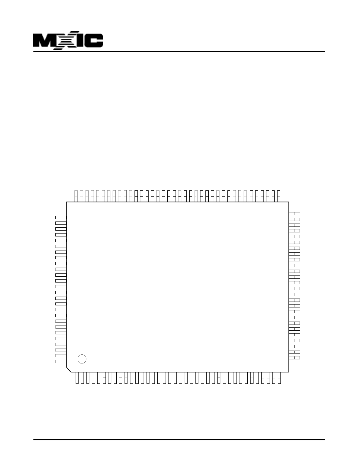
3. PIN CONFIGURATIONS
RTX
RTX2EQNCGND
TXOP
TXON
VDD
GND
GND
VDD
RXIP
RXIN
VDD
GND
VDD
GNDXOCKREF/XI
9998979695949392919089888786858483828180797877767574737271706968676665
102
101
100
VDD
GND
GND
VDD
GND
VDD
GND
LANWAKE
INTAB
RSTB
PCICLK
GNTB
REQB
AD31
AD30
GND
AD29
AD28
VDD
AD27
GND
AD26
AD25
GND
AD24
CBEB3
103
104
105
106
107
108
109
110
111
112
113
114
115
116
117
118
119
120
121
122
123
124
125
126
127
128
12345678910111213141516171819202122232425262728293031323334353637
MX98715AEC-C
The 32-bit multiplexed bus interface unit of
MX98715AEC-C provides a direct interface to a PCI local bus, simplifing the design of an Ethernet adapter in a
PC system. With its on-chip support for both little and
big endian byte alignment, MX98715AEC-C can also
address non-PC applications.
VDD
RDA
GND
VDD
LED1
LED0
BPA15
BPA14
BPA13
GND
VDD
BPA12
BPA11
BPA10
BPA9
BOEB
BPA8
BPA7
BPA6
BPA5
64
63
62
61
60
59
58
57
56
55
54
53
52
51
50
49
48
47
46
45
44
43
42
41
40
39
38
BPA4
BPA3
BPA2
BPA1(EEDI)
BPA0(EECK)
EECS
BPD0(EED0)
BPD1
BPD2
BPD3
BPD4
BPD5
BPD6
BPD7
GND
VDD
AD0
AD1
GND
AD2
AD3
VDD
AD4
AD5
GND
AD6
P/N:PM0655
GND
IDSEL
AD23
AD22
GND
AD21
AD20
VDD
AD19
AD18
GND
AD17
AD16
CBEB2
FRAMEB
GND
IRDYB
TRDYB
DEVSELSB
2
STOPB
VDD
PERRB
SERRB
PAR
AD15
CBEB1
GND
AD14
AD13
VDD
AD12
AD11
AD10
GND
AD9
AD8
AD7
CBEB0
REV. 0.3, MAY. 04, 2000
Page 3

MX98715AEC-C
4. PIN DESCRIPTION ( 128 PIN PQFP )
( T/S : tri-state, S/T/S : sustended tri-state, I : input, O : output, O/D : open drain )
Pin Name Type Pin No 128 Pin Function and Driver
AD[31:0] T/S 116, 117 PCI address/data bus: shared PCI address/data bus lines. Little or big endian
119,120, byte ordering are supported.
122,124,
125,127,
3,4,6,7,9,
10,12,13,
26,28,29,
31-33,35,
36,38,39,
41,42,44,
45,47,48
CBE[3:0] T/S 128,14 PCI command and b yte enable b us: shared PCI command b yte enable b us,
25,37 during the address phase of the transaction, these four bits provide the bus
command. During the data phase, these f our bits provide the b yte enab le.
FRAMEB S/T/S 15 PCI FRAMEB signal: shared PCI cycle start signal, asserted to indicate the
beginning of a bus transaction. As long as FRAMEB is asserted, data
transfers continue.
TRD YB S/T/S 18 PCI Target ready: issued b y the target agent, a data phase is completed on
the rising edge of PCICLK when both IRD YB and TRDYB are asserted.
IRD Y B S/T/S 17 PCI Master ready: indicates the bus master's ability to complete the current
data phase of the transaction. A data phase is completed on any rising edge
of PCICLK when both IRDYB and TRDYB are asserted.
DEVSELB S/T/S 19 PCI slave device select: asserted by the target of the current bus access.
When 98715A is the initiator of current bus access, the target must assert
DEVSELB within 5 bus cycles, otherwise cycle is aborted.
IDSEL I 1 PCI initialization device select: target specific de vice select signal f or
configuration cycles issued by host.
PCICLK I 1 1 3 PCI bus clock input: PCI bus clock range from 16MHz to 33MHz.
RSTB I 112 PCI bus reset: host system hardware reset.
LANWAKE O 110 Power Management Event:When high indicating a po wer management ev ent
occures, such as detection of a Magic packet, a wak e up frame, or link change.
INTAB O/D 111 PCI bus interrupt request signal: wired to INTAB line.
SERRB O/D 23 PCI bus system error signal: If an address parity error is detected and CFCS
bit 8 is enabled, SERRB and CFCS's bit 30 will be asserted.
PERRB S/T/S 22 PCI bus data error signal: As a b us master, when a data parity error is
detected and CFCS bit 8 is enabled, CFCS bit 24 and CSR5 bit 13 will be
asserted. As a bus target, a data parity error will cause PERRB to be
asserted.
P/N:PM0655
REV. 0.3, MAY. 04, 2000
3
Page 4

MX98715AEC-C
Pin Name Type Pin No 128 Pin Function and Driver
P AR T/S 24 PCI bus parity bit: shared PCI b us ev en parity bit for 32 bits AD bus and CBE
bus.
STOPB S/T/S 20 PCI Target requested transfer stop signal: as bus master , assertion of STOPB
cause MX98715AEC-C either to retry , disconnect, or abort.
REQB T/S 115 PCI bus request signal: to initiate a bus master cycle request
GNTB I 114 PCI bus grant acknowledge signal: host asserts to inform MX98715AEC-C
that access to the bus is granted
BPA1 O 6 1 Boot PROM address bit 1(EECS=0): together with BPA[15:0] to access
(EEDI) external boot PROM up to 256KB.
EEPROM data in(EECS=1): EEPROM serial data input pin.
BPA0 O 60 Boot PROM address bit 0(EECS=0): together with BPA[15:0] to access
(EECK) external boot PROM up to 256KB.
EEPROM clock(EECS=1): EEPR OM clock input pin
BPA[15:0] O 78-76,
73-70, Boot PROM address line.
68-60
BPD0 T/S 58 Boot PROM data line 0(EECS=0): boot PR OM or flash data line 0.
(EEDO) EEPROM data out(EECS=1): EEPROM serial data outpin(during reset
initialization).
BPD[7:0] T/S 51-58 Boot PR OM data lines: boot PROM or flash data lines 7-0.
EECS O 59 EEPROM Chip Select pin.
BOEB O 69 Boot PROM Output Enable .
RDA O 83 Connecting an external resistor to ground, Resistor value=10K ohms
RTX O 1 02 Connecting an external resistor to ground, Resistor value=560 ohms
RTX2EQ O 10 1 Connecting an external resistor to ground, Resister value=1.4K ohms
NC I 100 No Connection.
RXIP I 92 Twisted pair receive differential input: Support both 10 Base-T and 100
Base-TX receive differential input.
RXIN I 91 Twisted pair receive differential input: Support both 10 Base-T and 100
Base-TX receive differential input
TXOP O 98 T wisted pair tr ansmit differential output: Support both 10 Base-T and 100
Base-TX transmit differential output
TXON O 97 Twisted pair transmit differential output: Support both 10 Base-T and 100
Base-TX transmit differential output
XI/CKREF I 85 Reference clock: 25MHz oscillator cloc k input. For crystal application, This
pin is XI.
XO O 86 For crystal application, This pin is XO.
LED0 O 79 Programmable LED pin 0:
CSR9.28=1 Set the LED as Link Speed (10/100) LED .
CSR9.28=0 Set the LED as Activity LED .
Default is activity LED after reset.
P/N:PM0655
REV. 0.3, MAY. 04, 2000
4
Page 5

Pin Name Type Pin No 128 Pin Function and Driver
LED1 O 80 Programmable LED pin 1:
CSR9.29=1 Set the LED as Link/Activity LED .
CSR9.29=0 Set the LED as Good Link LED .
Default is Good Link LED after reset.
VDD I 8,21,30,43, Power pins.
49,74,81,84,
88,90,93,96,
103,106,108,
121
GND I 2,5,11,16,27 Ground pins.
34,40,46,50
75,82,87
89,94,95,99
104,105,107
109,118,123,
126
MX98715AEC-C
P/N:PM0655
REV. 0.3, MAY. 04, 2000
5
Page 6
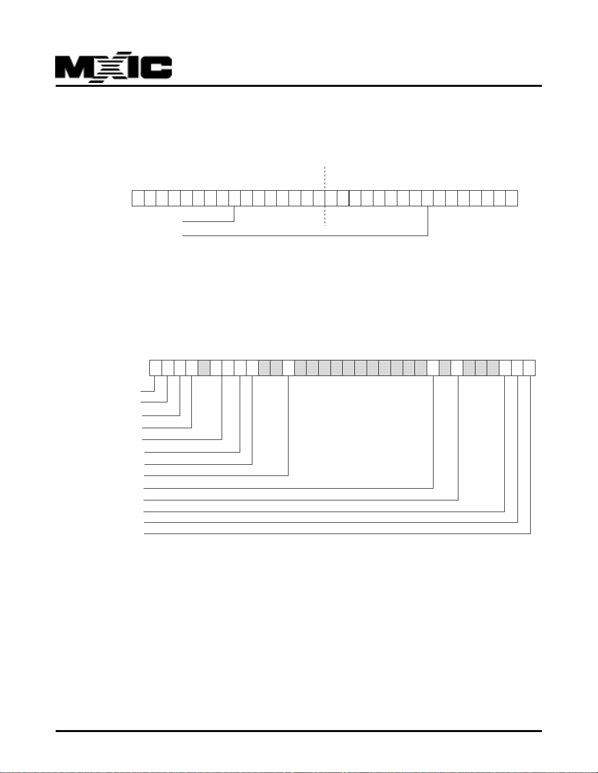
5. PROGRAMMING INTERFACE
5.1 PCI CONFIGURATION REGISTERS:
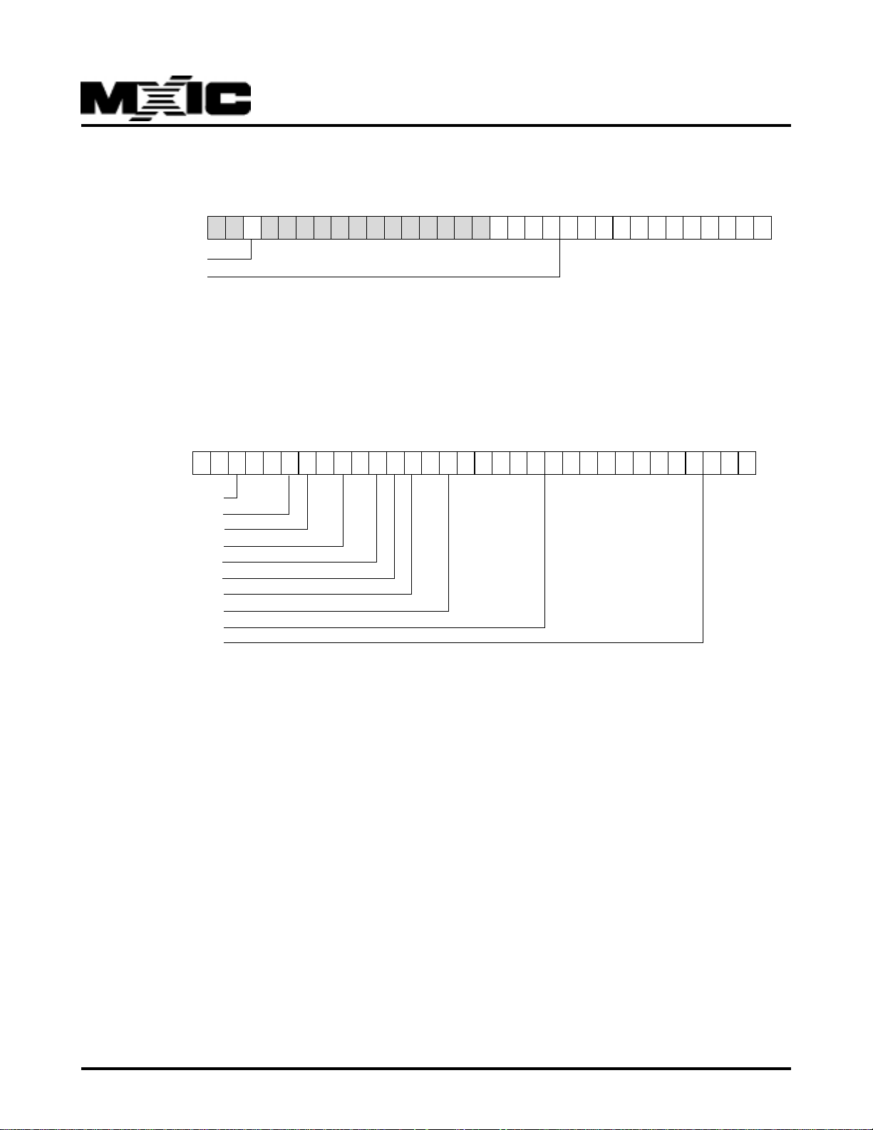
5.1.1 PCI ID REGISTER ( PFID ) ( Offset 03h-00h )
MX98715AEC-C
31 30 29 28 27 26 25 24 23 22 21 20 19 18 17 16
Device ID (bit 31:16)
Vendor ID (bit 15:0)
15 14 13 12 11 10 9 8 7 6 5 4 3 2 1 0
This register can be loaded from external serial EEPROM or use a MXIC preset value of "10D9" and "0531" for
vendor ID and device ID respectiv ely . W ord location 3Eh and 3Dh in serial EEPROM are used to configure customer's
vendor ID and device ID respectiv ely . If location 3Eh contains"FFFF" v alue then MXIC'svendor ID and device ID will
be set in this register, otherwise both 3Eh and 3Dh will be loaded into this register from serial EEPR OM.
5.1.2 PCI COMMAND AND STATUS REGISTER ( PFCS ) ( Offset 07h-04h )
31 30 29 28 27 26 25 24 23 22 21 20 19 18 17 16
Detect Party Error
Signal System Error
Receive Master Abort
Receive Target Abort
Device Select Timing
Data Parity Report
Fast Back-to-back
New Capability
System Error Enable
Parity Error Response
Master Operation
Memory Space Access
IO Space Access
15 14 13 12 11 10 9 8 7 6 5 4 3 2 1 0
The bit content will be reset to 0 when a 1 is written to the corresponding bit location.
bit 0 : IO Space Access , set to 1 enable IO access
bit 1 : Memory Space Access, set to 1 to enab le memory access
bit 2 : Master Operation, set to 1 to support bus master mode
bit 5-3 : not used
bit 6 : Parity Error Response, set to 1 to enable assertion of CSR<13> bit if parity error detected.
bit 7 : not used
bit 8 : System Error Enab le, set to 1 to enab le SERR# when parity error is detected on address lines and CBE[3:0].
bit 20 : Ne w capability. Set to support PCI power management.
bit 22-bit19 : not used
bit 23 : Fast Back-to bac k, alw a ys set to accept fast back-to-back transactions that are not sent to the same bus
device.
P/N:PM0655
6
REV. 0.3, MAY. 04, 2000
Page 7
MX98715AEC-C
bit 24:Data parity Report, is set to 1 only if PERR# active and PFCS<6> is also set.
bit 26-25:Device Select Timing of DEVSELB pin.
bit 27:not used
bit 28:Receive Target Abort, is set to indicate a transaction is terminated by a target abort.
bit 29:Receive Master Abort, is set to indicate a master transaction with Master abort.
bit 30:Signal System Error, is set to indicate assertion of SERR#.
bit 31:Detected Parity Error , is set whene v er a parity error detected regardless of PFCS<6>.
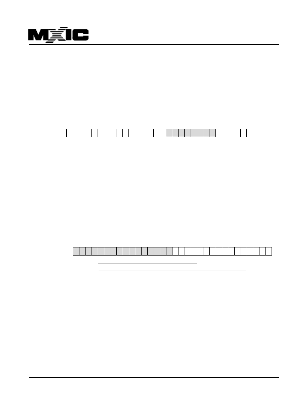
5.1.3 PCI REVISION REGISTER ( PFRV ) ( Offset 0Bh-08h )
31 30 29 28 27 26 25 24 23 22 21 20 19 18 17 16
Base Class
Subclass
Revision Number
Step Number
15 14 13 12 11 10 9 8 7 6 5 4 3 2 1 0
bit 3 - 0 : Step Number= 5h ( Previous MX98715 = 0h ).
bit 7 - 4 : Re vision Number , fix ed to 2h f or MX98715AEC-C
( Previous MX98715A series is also fixed to 2h )
bit 15 - 8 : not used
bit 23 - 16 : Subclass, fixed to 0h.
bit 31 - 24 : Base Class, fixed to 2h.
5.1.4 PCI LATENCY TIMER REGISTER ( PFLT ) (Offset 0Fh-0Ch)
PFLT Register (0Fh-0Ch)
31 30 29 28 27 26 25 24 23 22 21 20 19 18 17 16
Configuration Latency Timer
System cache line size
15 14 13 12 11 10 9 8 7 6 5 4 3 2 1 0
bit 0 - bit 7 : System cache line siz e in units of 32 bit word, device driver should use this value to prog ram CSR0<15:14>.
bit 8 - bit 15 : Configuration Latency Timer, when MX98715AEC-C assert FRAME#, it enables its latency timer to
count.
If MX98715AEC-C deasserts FRAME# prior to timer expiration, then timer is ignored. Otherwise , after timer expires,
MX98715AEC-C initiates transaction termination as soon as its GNT# is deasserted.
P/N:PM0655
7
REV. 0.3, MAY. 04, 2000
Page 8
MX98715AEC-C
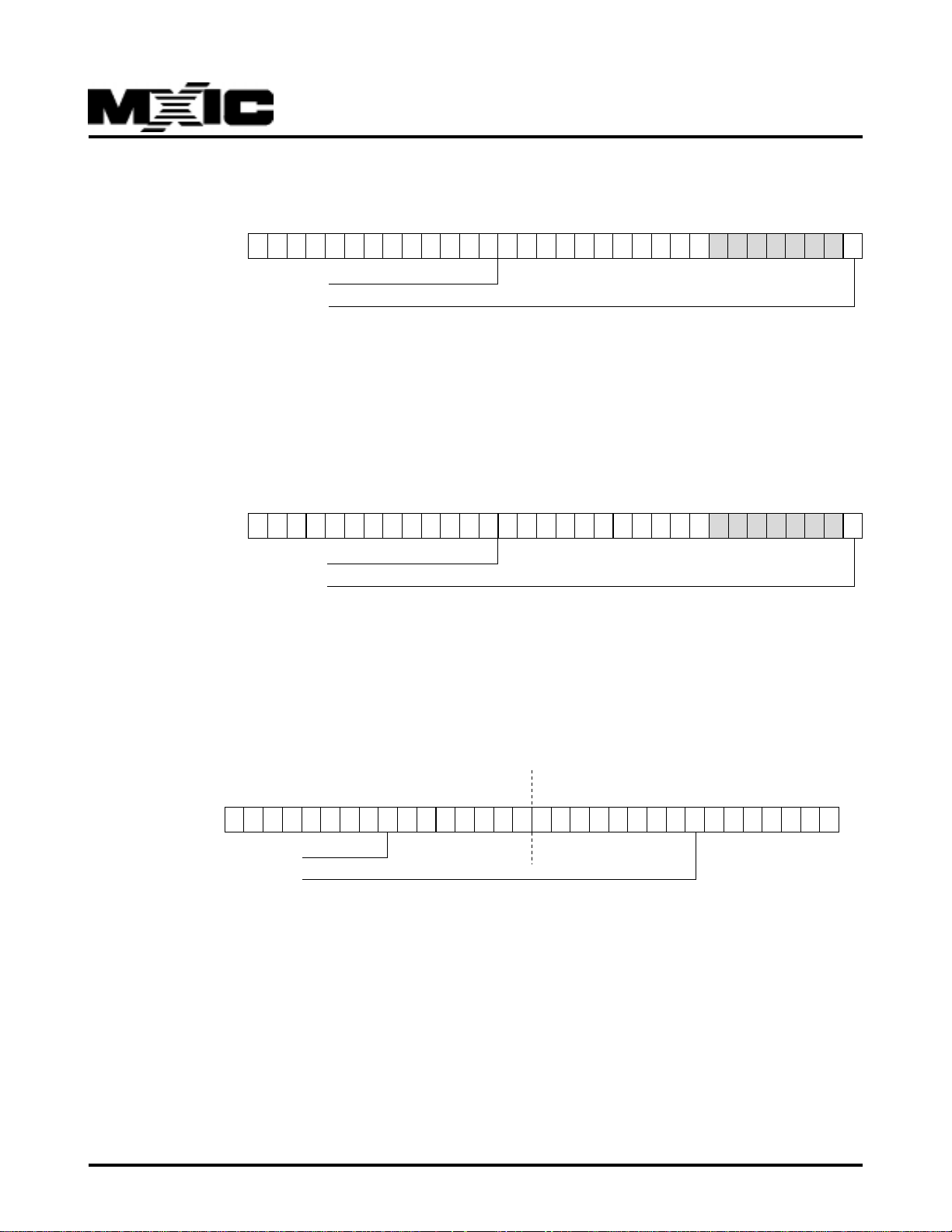
31 30 29 28 27 26 25 24 23 22 21 20 19 18 17 16
15 14 13 12 11 10 9 8 7 6 5 4 3 2 1 0
Configuration Base IO Address
IO/Memory Spec Indicator
5.1.5 PCI BASE IO ADDRESS REGISTER ( PBIO ) ( Offset 13h-10h )
bit 0 : IO/Memory Space Indicator , fix ed to 1 in this field will map into the IO space . This is a read only field.
bit 7 - 1 : not used, all 0 when read
bit 31 - 8 : Defines the address assignment mapping of MX98715AEC-C CSR registers.
5.1.6 PCI Base Memory Address Register ( PBMA ) ( Offset 17h-14h )
31 30 29 28 27 26 25 24 23 22 21 20 19 18 17 16
Configuration Base Memory Address
Memory Spec Indicator
15 14 13 12 11 10 9 8 7 6 5 4 3 2 1 0
bit 0 : Memory Space Indicator , fix ed to 0 in this field will map into the memory space. This is a read only field.
bit 6 - 1 : not used, all 0 when read
bit 31 - 7 : Defines the address assignment mapping of MX98715AEC-C CSR registers.
5.1.7 PCI SUBSYSTEM ID REGISTER ( PSID ) ( Offset 2Ch-2Fh )
31 30 29 28 27 26 25 24 23 22 21 20 19 18 17 16
Subsystem ID (31:16)
Subsystem Vendor ID (bit 15:0)
15 14 13 12 11 10 9 8 7 6 5 4 3 2 1 0
This register is used to uniquely identify the add-on board or subsystem where the NIC controller resides. V alues in
this register are loaded directly from external serial EEPROM after system reset automatically . W ord location 36h of
EEPROM is subsystem vendor ID and location 35h is sub-system ID.
P/N:PM0655
REV. 0.3, MAY. 04, 2000
8
Page 9

MX98715AEC-C
5.1.8 PCI BASE EXPANSION ROM ADDRESS REGISTER ( PBER ) ( Offset 33h-30h )
31 30 29 28 27 26 25 24 23 22 21 20 19 18 17 16
Expansion ROM Base Address (upper 21 bit)
Address Decode Enable
15 14 13 12 11 10 9 8 7 6 5 4 3 2 1 0
0 0 0 0 0 0 0
bit 0 : Address Decode Enabl e, decoding will be enabled if only both enable bit in PFCS<1> and this e xpansion ROM
register are 1.
bit 10 - 1 : not use
bit 31 - 11 : Defines the upper 21 bits of expansion ROM base address.
5.1.9 PCI CAPABILITY POINTER REGISTER ( PFCP ) ( Offset 37h-34h )
31 30 29 28 27 26 25 24 23 22 21 20 19 18 17 16
Capability Pointer (Set to 44h)
15 14 13 12 11 10 9 8 7 6 5 4 3 2 1 0
bit 7- 0 : Capability pointer (Cap_Ptr) is set to 44h if PMEB is connected to PCI b us , otherwise 00.
bit 31- 8 : reserve d
5.1.10 INTERRUPT REGISTER ( PFIT ) ( Offset 3Fh-3Ch )
31 30 29 28 27 26 25 24 23 22 21 20 19 18 17 16
0 0 1 1 1 0 0 0 0 0 0 0 1 0 0 0
Max_Lat
Min-Gnt
Interrupt Pin
Interrupt Line
15 14 13 12 11 10 9 8 7 6 5 4 3 2 1 0
bit 7 - 0 : Interrupt Line, system BIOS will writes the routing inf ormation into this field, driver can use this information
to determine priority and interrupt vector.
bit 15 - 8 : Interrupt Pin, fix ed to 01h which use INTA#.
bit 31 - 24 : Max_Lat which is a maximum period f or a access to PCI b us .
bit 23 - 16 : Min_Gnt which is the maximum period that MX98715AEC-C needs to finish a brust PCI cycle.
P/N:PM0655
REV. 0.3, MAY. 04, 2000
9
Page 10
5.1.11 PCI DRIVER AREA REGISTER ( PFDA ) ( 43h-40h )
MX98715AEC-C
31 30 29 28 27 26 25 24 23 22 21 20 19 18 17 16
Board T ype
Driver Special Use
15 14 13 12 11 10 9 8 7 6 5 4 3 2 1 0
bit 29 : board type
bit 15 - 8 : driver is free to read and write this field for an y purpose.
bit 7 - 0 : not used.
5.1.12 PCI POWER MANAGEMENT CAPABILITY REGISTER ( PPMC ) ( 47h-44h )
31 30 29 28 27 26 25 24 23 22 21 20 19 18 17 16
PME_Support
D2_Support
D1_Support
AUX_I
DSI
Auxiliary Power Source
PME Clock
Version
Next Pointer
Capability ID
15 14 13 12 11 10 9 8 7 6 5 4 3 2 1 0
0 0 0 0 0 0 0 0
bit 31- 27 : PME_Support, read only indicates the power states in which the function ma y assert LANWAKE pin.
bit 31 ---- PME_D3cold (value=1)
bit 30 ---- PME_D3warm (value=1)
bit 29 ---- PME_D2 (value=1)
bit 28 ---- PME_D1 (value=1)
bit 27 ---- PME_D0 (value=1)
bit 26 : D2 mode support, read only, set to 1.
bit 25 : D1 mode support, read only, set to 1.
bit 24-22 : AUX_I bits. Auxiliary current field, set to 100.
bit 21 : DSI, read only, set to 0.
bit 20 : Auxiliary power source, set to 1. This bit only valid when bit 15 is a '1'.
bit 19 : PME Cloc k, read only, set to 0.
bit 18-16 : PCI po wer management v ersion, set to 001, read only.
bit 15-8 : Ne xt Pointer, all bits set to 0.
bit 7-0 : Capability ID, read only, a 1 indicates that the data structure currently being pointed to is the PCI pow er
managment data structure.
P/N:PM0655
10
REV. 0.3, MAY. 04, 2000
Page 11

MX98715AEC-C
5.1.13 PCI POWER MANAGEMENT COMMAND AND STATUS REGISTER ( PPMCSR ) ( 4Bh-48h )
31 30 29 28 27 26 25 24 23 22 21 20 19 18 17 16
Data
Bridge Extension Support
PME_Status
Data_Scale
Data_Select
PME_EN
Reserved
Power State
15 14 13 12 11 10 9 8 7 6 5 4 3 2 1 0
0 0 0 0 0 0
bit 1-0 : Power_State , read/write, D0 mode is 00, D1 mode is 01, D2 mode is 10, D3 hot mode is 11.
bit7-2 : all 0. Reserved.
bit8 : PME_EN, set 1 to enab le LANWAKE. Set 0 to disable LANW AKE assertion.
bit 12-9 : Data_Select f or report in the Data register located at bit 31:24.
bit 14-13 : Data_Scale, read only.
bit 15 : PME_Status independent of the state of PME_EN.
When set, indicates a assertion of LANWAKE pin. (support D3 cold).
Write 1 to clear the LANWAKE signal. Write 0, no eff ect.
bit 21-16 : Reserved.
bit 22 : B2_B3#, B2_B3 support for D3 hot, meaningful only if BPCC_EN = 1, read only.
bit 23 : BPCC_EN, Bus Power/Clock Control Enable, read only.
bit 31-24 : Data, read only.
P/N:PM0655
REV. 0.3, MAY. 04, 2000
11
Page 12

MX98715AEC-C
5.2 HOST INTERF ACE REGISTERS
MX98715AEC-C CSRs are located in the host I/O or memory address space. The CSRs are double word aligned and
32 bits long. Definitions and address for all CSRs are as follows :
CSR Mapping
Register Meaning Offset from CSR Base
Address ( PBIO and PBMA )
CSR0 Bus mode 0 0
CSR1 T ransmit poll demand 08 h
CSR2 Receive poll demand 10 h
CSR3 Receive list demand 18 h
CSR4 T ransmit list base address 20 h
CSR5 Interrupt status 28 h
CSR6 Operation mode 30h
CSR7 Interrupt enable 38 h
CSR8 Missed frame counter 40 h
CSR9 Serial ROM and MII management 48h
CSR10 Reserved 50h
CSR11 General Purpose timer 58 h
CSR12 10 Base-T status port 60h
CSR13 SIA Reset Register 68 h
CSR14 10 Base-T control port 70h
CSR15 Watchdog timer 7 8h
CSR20 Auto compensation A0h
CSR21 Flow control Register A8h
CSR22 MAC ID Byte 3-0 B0h
CSR23 Magic ID 5, 4 / MAC ID Byte 5, 4 B8h
CSR24 Magic ID Byte 3-0 C0h
CSR25 Filter 0 Byte Mask C8h
CSR26 Filter 1 Byte Mask D0h
CSR27 Filter 2 Byte Mask D8h
CSR28 Filter 3 Byte mask E0h
CRS29 Filter Offset E8h
CSR30 Filter 1&0 CRC-16 F0h
CSR31 Filter 3&2 CRC-16 F8h
P/N:PM0655
REV. 0.3, MAY. 04, 2000
12
Page 13

5.2.1 BUS MODE REGISTER ( CSR0 )
MX98715AEC-C
31 30 29 28 27 26 25 24 23 22 21 20 19 18 17 16
WIE-Write and Invalidate Enable
RLE-Read Line Enable
RME-Read Multiple Enable
TAP-Transmit Automatic Polling
ZERO-Must be zero
CAL-Cache Alignment
PBL-Programmable Burst Length
BLE-Big/Little Endian
DSL-Descriptor Skip Length
BAR0-Bus Arbitration bit 0
SWR-Software Reset
15 14 13 12 11 10 9 8 7 6 5 4 3 2 1 0
Field Name Description
0 SW R Software Reset, when set, MX98715AEC-C resets all internal hardware with the exception
of the configuration area and port selection.
1 BAR0 Internal bus arbitration scheme between receive and transmit processes.
The receive channel usually has higher priority over transmit channel when receiv e FIFO
is partially full to a threshold. This threshold can be selected b y programming this bit. Set
for lower threshold, reset for normal threshold.
6:2 DSL Descriptor Skip Length, specifies the number of longwords to skip between two descrip-
tors.
7 BLE Big/Little Endian, set for big endian byte ordering mode, reset for little endian b yte order-
ing mode, this option only applies to data buff ers
13:8 PBL Programmable Burst Length, specifies the maximum number of longwords to be trans-
ferred in one DMA transaction. default is 0 which means unlimited burst length, possible
values can be 1,2,4,8,16,32 and unlimited .
15:14 CAL Cache Alignment, programmable address boundaries of data burst stop, MX98715AEC-C
can handle non-cache- aligned fragement as well as cache-aligned fragment efficiently .
18:17 T AP T ransmit Auto-Polling time interval, defines the time interval for MX98715AEC-C to per-
forms transmit poll command automatically at transmit suspended state.
21 RME PCI Memor y Read Multiple command enable, indicates bus master may intend to fetch
more than one cache lines disconnecting.
23 RLE PCI Memory Read Line command enable, indicating bus master intends to fetch a com-
plete cache line.
24 WLE PCI Memory Write and Invalidate command enable, guarantees a minimum transfer of
one complete cache.
P/N:PM0655
REV. 0.3, MAY. 04, 2000
13
Page 14

MX98715AEC-C
TABLE 5.2.0 TRANSMIT AUTO POLLING BITS
CSR<18:17> Time Interval
00 No transmit auto-polling, a write to CSR1 is required to poll
01 auto-poll every 200 us
10 auto-poll every 800 us
11 auto-poll every 1.6 ms
5.2.2 TRANSMIT POLL COMMAND ( CSR1 )
31 30 29 28 27 26 25 24 23 22 21 20 19 18 17 16
Transmit Poll command
15 14 13 12 11 10 9 8 7 6 5 4 3 2 1 0
Field Name Description
31:0 TPC Write only , when written with any value , MX98715AEC-C read transmit descriptor list in
host memory pointed by CSR4 and processes the list.
5.2.3 RECEIVE POLL COMMAND ( CSR2 )
31 30 29 28 27 26 25 24 23 22 21 20 19 18 17 16
Receive Poll command
15 14 13 12 11 10 9 8 7 6 5 4 3 2 1 0
Field Name Description
31:0 RPC Write only , when written with any value, MX98715AEC-C read receive descriptor list in host
memory pointed by CSR3 and processes the list.
P/N:PM0655
REV. 0.3, MAY. 04, 2000
14
Page 15

5.2.4 DESCRIPTOR LIST ADDRESS ( CSR3, CSR4 )
CSR3 Receive List Base Address
MX98715AEC-C
31 30 29 28 27 26 25 24 23 22 21 20 19 18 17 16
Start of Receive List Address
CSR4 Transmit List Base Address
31 30 29 28 27 26 25 24 23 22 21 20 19 18 17 16
Start of Transmit List Address
15 14 13 12 11 10 9 8 7 6 5 4 3 2 1 0
15 14 13 12 11 10 9 8 7 6 5 4 3 2 1 0
P/N:PM0655
REV. 0.3, MAY. 04, 2000
15
Page 16

5.2.5 STATUS REGISTER ( CSR5 )
MX98715AEC-C
31 30 29 28 27 26 25 24 23 22 21 20 19 18 17 16
WKUPI-Wake Up event Interrupt
LC-Link Change
EB-Error Bits
TS-Transmit Process State
RS-Receive Process State
NIS-Normal Interrupt Summary
AIS-Abnormal Interrupt Summary
ERI-Early Receive Interrupt
FBE-Fatal Bus Error
LF-Link Fail
GTE-General Purpose Timer Expired
ETI-Early T ransmit Interrupt
RWT-Receive Watchdog Timeout
RPS-Receive Process Stopped
RU-Receive Buffer Unavailable
RI-Receive Interrupt
LPANCI-Link Pass/Autonegotiation
Completed Interrupt
UNF-Transmit Underflow
TJT-Transmit Jabber Timeout
TU-Transmit Buffer Unavailable
TPS-Transmit Process Stopped
TI-Transmit Interrupt
15 14 13 12 11 10 9 8 7 6 5 4 3 2 1 0
Field Name Description
28 WKUPI Wake Up ev ent interrupt. Valid only if CSR16<22> bit is set.
27 LC 100 Base-TX link status has changed either from pass to fail or f ail to pass.
Read CSR12<1> for 100 Base-TX link status.
25:23 EB Error Bits , read only, indicating the type of error that caused fatal bus error .
22:20 TS Transmit Process State, read only bits indicating the state of transmit process.
19:17 RS Receive Process State , read only bits indicating the state of receiv e process .
16 NIS Normal Interrupt Summary, is the logical OR of CSR5<0>, CSR5<2> and CSR5<6> and
CSR5<28>.
15 AIS Abnormal Interrupt Summary, is the logical OR of CSR5<1>, CSR5<3>, CSR5<5>,
CSR5<7>, CSR5<8>, CSR5<9>, CAR5<10>, CSR5<11> and CSR5<13>, CSR5<27>.
14 ERI Early receive interrupt, indicating the first buffer has been filled in ring mode, or 64 bytes
has been received in chain mode.
1 3 FBE Fatal Bus Error , indicating a system error occured, MX98715AEC-C will disable all bus
access.
1 2 LF Link Fail, indicates a link fail state in 10 Base-T port. This bit is valid only when
CSR6<18>=0, CSR14<8>=1, and CSR13<3>=0.
11 GTE General Purpose Timer Expired, indicating CSR11 counter has e xpired.
P/N:PM0655
16
REV. 0.3, MAY. 04, 2000
Page 17

MX98715AEC-C
Field Name Description
10 ETI Early Transmit Interrupt, indicating the packet to be transmitted was fully transferred to
internal TX FIFO. CSR5<0> will automatically clear this bit.
9 RWT Receive Watchdog Timeout, reflects the network line status where receiv e watchdog
timer has expired while the other node is still active on the netw ork.
8 RPS Write only , when written with any value, MX98715AEC-C reads receiv e descriptor list in
host memory pointed by CSR4 and processes the list.
7 RU Receive Buffer Unavailable, the receive process is suspended due to the next
descriptor in the receive list is owned by host. If no receive poll command is issued, the
reception process resumes when the next recognized incoming frame is receiv ed.
6 RI Receive Interrupt, indicating the completion of a frame reception.
5 UNF Transmit Underflow, indicating transmit FIFO has run empty bef ore the completion of a
packet transmission.
4 LPANCI When autonegotiation is not enabled ( CSR14<7>=0 ), this bit indicates that the 10
Base-T link integrity test has completed successfully, after the link was down. This bit is
also set as as a result of writing 0 to CSR14<12> ( Link Test Enable ).
When Autonegotiation is enabled ( CSR14<7> =1 ) , this bit indicates that the autonegotiation
has completed ( CSR12<14:12>=5 ). CSR12 should then be read f or a link status report.
This bit is only valid when CSR6<18>=0, i.e. 10 Base-T port is selected Link Fail interrupt
( CSR5<12> ) will automatically clears this bit.
3 TJT T r ansmit Ja bber Timeout, indicating the MX98715 has been excessively active. The
transmit process is aborted and placed in the stopped state. TDES0<1> is also set.
2 TU Transmit Buffer Unavailable, transmit process is suspended due to the next descriptor in
the transmit list is owned by host.
1 TPS Transmit Process Stopped.
0 TI Transmit Interrupt. indicating a frame transmission was completed.
P/N:PM0655
REV. 0.3, MAY. 04, 2000
17
Page 18

MX98715AEC-C
TABLE 5.2.1 FATAL BUS ERROR BITS
CSR5<25:23> Process State
000 parity error for either SERR# or PERR#, cleared by software reset.
001 master abort
010 target abort
011 reserved
1XX reserved
TABLE 5.2.2 TRANSMIT PROCESS ST ATE
CSR5<22:20> Process State
000 Stopped- reset or transmit jabber expired.
001 Fetching transmit descriptor
010 Waiting f or end of transmission
011 filling transmit FIFO
100 reserved
101 Setup packet
110 Suspended, either FIFO underflow or unavailab le transmit descriptor
111 closing transmit descriptor
TABLE 5.2.3 RECEIVE PROCESS STAT E
CSR5<19:17> Process State
000 Stopped- reset or stop receive command. Fetching receive descriptor
010 checking for end of receive pac k et
011 Waiting f or receive pac ket
100 Suspended, receive buff er unav ailable
101 closing receive descriptor
110 Purging the current frame from the receive FIFO due to unav ailab le receiv e b uff er
111 queuing the receive frame from the receive FIFO into host receiv e b uffer
P/N:PM0655
REV. 0.3, MAY. 04, 2000
18
Page 19

5.2.6 OPERATION MODE REGISTER ( CSR6 )
MX98715AEC-C
31 30 29 28 27 26 25 24 23 22 21 20 19 18 17 16
SCR-Scrambler Mode
PCS-PCS function
TTM-T ransmit Threshold Mode
SF-Store and Forward
HBD-Hearbeat Disable
PS-Port Select
COE-Collision Offset Enable
TR-Threshold Control Bits
ST-Start/Stop T ransmission Command
FC-Force collision mode
LOM-Loopback Operation Mode
FD-Full Duplex Mode
PM-Pass All Multicast
PR-Promiscuous Mode
SB-Start/Stop Backoff Counter
IF-Inverse Filtering
PB-Pass Bad Frame
HO-Hash-Only Filtering Mode
SR-Start/Stop Receive
HP-Hash/Perfect Receive Filtering Mode
15 14 13 12 11 10 9 8 7 6 5 4 3 2 1 0
Field Name Description
24 SCR Scrambler Mode, default is set to enab le scramb ler function. Not affected by software
reset.
23 PCS Default is set to enable PCS functions. CSR6<18> m ust be set in order to operate in
symbol mode.
22 TTM T ransmit Threshold Mode, set for 10 Base-T and reset for 100 Base-TX.
21 SF Store and Forward, when set, transmission starts only if a full packet is in transmit FIFO.
the threshold values defined in CSR6<15:14> are ignored
19 HBD Heartbeat Disable, set to disable SQE function in 10 Base-T mode.
18 PS Port Select, deafult is 0 which is 10 Base-T mode, set for 100 Base-TX mode .
A software reset does not affect this bit.
17 COE Collision Offset Enable, set to enable a modified back off algorithm during low collision
situation, reset for normal backoff algorithm.
15:14 TR Threshold Control Bits, these bits controls the selected threshold level for MX98715AEC-
C's transmit FIFO, tr ansmission starts when frame size within the transmit FIFO is larger
than the selected threshold. Full frames with a length less than the threshold are also
transmitted.
P/N:PM0655
REV. 0.3, MAY. 04, 2000
19
Page 20

MX98715AEC-C
Field Name Description
13 ST Start/Stop Transmission Command, set to place transmission process in running state
and will try to transmit current descriptor in transmit list. When reset, tr ansmit process is
placed in stop state.
12 FC Force Collision Mode, used in collision logic test in internal loopback mode, set to force
collision during next transmission attempt. This can result in e xcessiv e collision reported
in TDES0<8> if 16 or more collision.
11:10 LOM Loopback Operation Mode , see table 5.2.6.
9 FD Full-Duplex Mode, set f or simultaneous transmit and receiv e oper ation, heart beat check
is disabled, TDES0<7> should be ignored, and internal loopback is not allow ed. This bit
controls the value of bit 6 of link code word .
7 PM Pass All Multicast, set to accept all incoming frames with a multicast destination address
are received. Incoming frames with physical address are filtered according to the CSR6<0>
bit.
6 PR Promiscuous Mode, an y incoming v alid frames are accepted, def ault is reset and not
affected by softw are reset.
5 SB Start/Stop Backoff Counter, when reset, the backoff timer is not aff ected b y the netw ork
carrier activity . Otherwise, timer will start counting when carrier drops.
4 IF Inverse Filtering, read only bit, set to operate in inv erse filtering mode, only valid during
perfect filtering mode.
3 PB Pass Bad F rames , set to pass bad frame mode , all incoming frames passed the address
filtering are accepted including runt frames, collided fragments, truncated frames caused
by FIFO overflo w.
2 HO Hash-Only Filtering Mode , read only bit, set to operate in imperfect filtering mode for both
physical and multicast addresses .
1 SR Start/Stop Receive, set to place receiv e process in running state where descriptor
acquisition is attempted from current position in the receive list. Reset to place the
receive process in stop state.
0 HP Hash/P erfect Receive Filtering Mode, read only bit, set to use hash tab le to filter multicast
incoming frames. If CSR6<2> is also set, then the physical addresses are
imperfect address filtered too . If CSR6<2> is reset, then physical addresses are perfect
address filtered, according to a single physical address as specified in setup frame.
P/N:PM0655
REV. 0.3, MAY. 04, 2000
20
Page 21

MX98715AEC-C
TABLE 5.2.4 TRANSMIT THRESHOLD
CSR6<21> CSR6<15:14> CSR6<22>=0 CSR6<22>=1 (Threshold bytes)
(for 100 Base-TX) (for 10 Base-T)
0 00 128 72
0 01 256 96
0 10 512 128
0 11 1024 160
1 XX ( Store and Forward )
TABLE 5.2.5 DATA PORT SELECTION
CSR14<7> CSR6<18> CSR6<22> CSR6<23> CSR6<24> Port
1 0 X X 1 Nway A uto-negotiation
0 0 1 X 0 10 Base-T
0 1 0 1 X 100 Base-TX
TABLE 5.2.6 LOOPBACK OPERATION MODE
CSR6<11:10> Operation Mode
00 Normal
01 Internal loopback at FIFO port
11 Internal loopback at the PHY level
10 External loopback at the PMD level
TABLE 5.2.7 FILTERING MODE
CSR6<7> CSR6<6> CSR6<4> CSR6<2> CSR6<0> Filtering Mode
0 0 0 0 0 16 perfect filtering
0 0 0 0 1 128-bit hash + 1 perfect filtering
0 0 0 1 1 128-bit hash for multicast and
physical addresses
0 0 1 0 0 Inverse filtering
X 1 0 0 X Promiscuous
0 1 0 1 1 Promiscuous
1 0 0 0 X Pass All Multicast
1 0 0 1 1 Pass All Multicast
P/N:PM0655
REV. 0.3, MAY. 04, 2000
21
Page 22

5.2.7 INTERRUPT MASK REGISTER ( CSR7 )
MX98715AEC-C
31 30 29 28 27 26 25 24 23 22 21 20 19 18 17 16
WKUPIE-Wake Up event interrupt Enable
LCE-Link Changed Enable
NIE-Normal interrupt Summary Enable
AIE-Abnormal Interrupt Summary Enable
ERIE-Early Receive Interrupt Enable
FBE-Fatal Bus Error Enable
LFE-Link Fail Enable
GPTE-General-Purpose Timer Enable
ETIE-Early Transmit Interrupt Enable
RWE-Receive Watchdog Enable
RSE-Receive Stopped Enable
RUE-Receive Buffer Unavailable Enable
RIE-Receive Interrupt Enable
UNE-Underflow Interrupt Enable
LPANCIE-Link Pass
/Nway Complete Interrupt Enable
TJE-Transmit Jabber Timeout Enable
TUE-Transmit Buffer Unavailable Enable
TSE-Transmit Stopped Enable
TIE-Transmit Interrupt Enable
15 14 13 12 11 10 9 8 7 6 5 4 3 2 1 0
Field Name Description
28 WKUPIE Wake Up Ev ent Interrupt Enable , enables CSR5<28>.
27 LCE Link Changed Enable, enab les CSR5<27>.
16 NIE Normal Interrupt Summary Enable, set to enable CSR5<0>, CSR5<2>, CSR5<6>.
15 AIE Abnormal Interrupt Summary enable, set to enbale CSR5<1>, CSR5<3>, CSR5<5>,
CSR5<7>, CSR5<8>, CSR5<9>, CSR5<11> and CSR5<13>.
14 ERIE Early Receive Interrupt Enable
13 FBE F atal Bus Error Enab le , set together with with CSR7<15> enables CSR5<13>.
12 LFE Link Fail Interrupt Enable , enables CSR5<12>
11 GPTE General Purpose Timer Enable , set together with CSr7<15> enables CSR5<11>.
10 ETIE Early Transmit Interrupt Enable, enables CSR5<10>
9 RWE Receive W atchdog Timeout Enable, set together with CSR7<15> enables CSR5<9>.
8 RSE Receive Stopped Enable, set together with CSR7<15> enables CSR5<8>.
7 RU E Receive Buffer Unavailab le Enable , set together with CSR7<15> enables CSR5<7>.
6 RIE Receive Interrupt Enable, set together with CSR7<16> enab les CSR5<6>.
5 UNE Underflow Interrupt Enable, set together with CSR7<15> enables CSR5<5>.
4 LPANCIE Link P ass/Autonegotiation Completed Interrupt Enab le
3 TJE Transmit Jabber Timeout Enable , set together with CSR7<15> enables CSR5<3>.
2 TUE T ransmit Buff er Unav ailable Enab le, set together with CSR7<16> enab les CSR5<2>.
1 TSE Transmit Stop Enable , set together with CSR7<15> enables CSR5<1>.
0 TIE Transmit Interrupt Enable, set together with CSR7<16> enables CSR5<0>.
P/N:PM0655
REV. 0.3, MAY. 04, 2000
22
Page 23

5.2.8 MISSED FRAME COUNTER ( CSR8 )
MX98715AEC-C
31 30 29 28 27 26 25 24 23 22 21 20 19 18 17 16
Missed Frame Overflow
Missed Frame Counter
15 14 13 12 11 10 9 8 7 6 5 4 3 2 1 0
Field Name Description
16 MFO Missed Frame Ov erflow, set when missed frame counter overflows, reset when CSR8
is read.
15:0 MFC Missed Frame Counter , indicates the number of fr ames discarded because no host
receive descriptors were av ailable .
5.2.9 NON-VOLATILE MEMORY CONTROL REGISTER ( CSR9 )
31 30 29 28 27 26 25 24 23 22 21 20 19 18 17 16
LED3SEL
LED2SEL
LED1SEL
LED0SEL
WKFCAT
LED4SEL
RD-Read Operation
Reload
BR-Boot ROM Select
SR-Serial ROM Select
Data-Boot ROM data
or Serial ROM control
15 14 13 12 11 10 9 8 7 6 5 4 3 2 1 0
Field Name Description
31 LED3SEL 0:Default value. Set LED3 as RX LED.
1:Set LED3 as F/H duplex LED . (LED3 is not bonded to pin )
30 LED2SEL 0: Default value. Set LED2 as SPEED LED.
1: Set LED2 as Collision LED (LED2 is not bonded to pin)
29 LED1SEL 0:Default value. Set LED1 as Good Link LED.
1: Set LED1 as Link/Activity LED.
28 LED0SEL 0:Default value. Set LED0 as Activity LED.
1: Set LED0 as Link Speed (10/100) LED .
24 *LED4SEL 0: Default value. Set LED4 as Collison LED.
1: Set LED4 as PMEB LED. (LED4 is not bonded to pin)
1 4 R D Boot ROM read operation when boot ROM is selected.
P/N:PM0655
23
REV. 0.3, MAY. 04, 2000
Page 24

MX98715AEC-C
26:25 WKF ACT Wake up frame catenation option bits.
CRS21<4> CSR<26> CSR<25> Wake up event
0 X X CH0+CH1+CH2+CH3
1 0 0 (CH0.CH1)+(CH2.CH3)
1 0 1 (CH0.CH1)+CH2+CH3
1 1 0 (CH0.CH1.CH2)+CH3
1 1 1 CH0.CH1.CH2.CH3
13 Reload EEPROM re-load operation select bit.
Operation definition:
RD Reload Operation
1 0 Boot ROM/EEPROM Read
1 1 EEPROM re-load operation (SR=1)
1 2 BR Boot ROM Select, set to select boot ROM only if CSR9<11>=0.
1 1 SR Serial ROM Select, set to select serial ROM for either read or write operation.
Field Name Description
7:0 Data If boot ROM is selected ( CSR9<12> is set ), this field contains the data to be read from
and written to the boot ROM. If serial ROM is selected , CSR9<3:0> are defined as
follows :
3 SDO Serial ROM data out from serial ROM into MX98715AEC-C.
2 SDI Serial ROM data input to serial ROM from MX98715AEC-C.
1 SCLK Serial clock output to serial ROM.
0 SCS Chip select output to serial ROM.
Warning : CSR9<11> and CSR9<12> should be m utually exclusiv e for correct operations.
01
LED0SEL ACT SPEED
LED1SEL LINK LINK/ACT
LED2SEL SPEED CO L
LED3SEL RX FULL/HALF
LED4SEL* CO L PMEB
<Note> LED4SEL is only valid in MX98715B
5.2.10 GENERAL PURPOSE TIMER ( CSR11 )
31 30 29 28 27 26 25 24 23 22 21 20 19 18 17 16
CON-Continuous Mode
Timer Value
15 14 13 12 11 10 9 8 7 6 5 4 3 2 1 0
Field Name Description
16 CON When set,the general purpose timer is in continuous operating mode. When reset, the
timer is in one-shot mode.
15:0 Timer Value contains the timer value in a cycle time of 204.8us.
P/N:PM0655
24
REV. 0.3, MAY. 04, 2000
Page 25

5.2.11 10 BASE-T STATUS Port ( CSR12 )
MX98715AEC-C
31 30 29 28 27 26 25 24 23 22 21 20 19 18 17 16
LPC-Link Partner's Link Code Word
LPN-Link Partner Negotiable
ANS-Autonegotiation Arbitration State
TRF-Transmit Remote Fault
APS-Autopolarity State
LS10B-Link Status of 10 Base-T
LS100B-Link Status of 100 Base-TX
*Software reset has no effect on this register
15 14 13 12 11 10 9 8 7 6 5 4 3 2 1 0
Field Name Decription
31:16 LPC Link P artner's Link Code W ord, where bit 16 is S0 ( selector field bit 0 ) and bit31 is NP
( Next P age ). Effectiv e only when CSR12<15> is read as a logical 1.
15 LPN Link Partner Negotiable, set when link partner support NWAY algorithm and CSR14<7>
is set.
14:12 ANS Autonegotiation Arbitration State , arbitration states are defined
000 = Autonegotiation disable
001 = Transmit disable
010 = ability detect
011 = Acknowledge detect
100 = Complete acknowledge detect
101 = FLP link good; autonegotiation complete
110 = Link check
When autonegotiation is completed, an ANC interrupt ( CSR5<4>) is generated, write
001 into this field can restart the autonegotiation sequence if CSR14<7> is set.
Otherwise, these bits should be 0.
11 TRF Transmit Remote Fault
3 APS Autopolarity State, set when polarity is positive. When reset, the 10Base-T polarity is
negative. The received bit stream is inverted by the receiver.
2 LS10B Set when link status of 10 Base-T port link test fail. Reset when 10 Base-T link test is in
pass state.
1 LS100B Link state of 100 Base-TX, this bit reflects the state of SD pin, effective only when
CSR6<23>= 1 ( PCS is set ). Set to indicate a f ail condition .i.e . SD=0.
P/N:PM0655
25
REV. 0.3, MAY. 04, 2000
Page 26

5.2.12 SIA Reset Register (CSR13)
MX98715AEC-C
31 30 29 28 27 26 25 24 23 22 21 20 19 18 17 16
100 TX Reset-
100 Base-TX PHY level reset
Nway Reset-
Nway and 10 Base-T PHY level reset
15 14 13 12 11 10 9 8 7 6 5 4 3 2 1 0
Field Name Decription
0 Nway Reset While writing 0 to this bit, resets the CSR12 & CSR14.
1 100Base-TX Reset Write a 1 will reset the internal 100 Base-TX PHY module
5.2.13 10 Base-T Control PORT (CSR14)
31 30 29 28 27 26 25 24 23 22 21 20 19 18 17 16
PAUSE-Pause (link code word)
T4-100 Base-T4 (link code word)
TXF-100 Base-TX full duplex
(link code word)
TXH-100 Base-TX half duplex
(link code word)
L TE-Link Test Enable
RSO-Receive Squelch Enable
ANE-Autonegotiation Enable
HDE-Half Duplex Enable)
PWD10B-Power down 10 Base-T
LBK-Loopback (MCC)
15 14 13 12 11 10 9 8 7 6 5 4 3 2 1 0
*The software reset bit (bit0 of CSR0) has no effect to this register.
Field Name Decription
19 PAUSE Bit 10 of link code word for 100 Base-TX pause mode.
18 T4 Bit 9 of link code w ord for T4 mode .
17 TXF Bit 8 of link code word for 100 Base-TX full duplex mode.
16 TXH Bit 7 of link code word for 100 Base-TX half duplex mode. Meaningful only when CSR14<7>
( ANE ) is set.
12 LTE Link Test Enable, when set the 10 Base-T port link test function is enabled.
8 RSQ Receive Squelch Enable f or 10 Base-T port. Set to enab le .
7 ANE Autonegotiation Enable , .
6 HDE Half-Duplex Enable, this is the bit 5 of link code word, only meaningful when CSR14<7> is
set.
2 PWD10B Reset to power down 10 Base-T module, this will f orce both TX and RX port into tri-state
and prevent A C current path. Set for normal 10 Base T operation.
1 LBK Loop back enable for 10 Base-T MCC .
P/N:PM0655
26
REV. 0.3, MAY. 04, 2000
Page 27

MX98715AEC-C
5.2.14 WATCHDOG TIMER ( CSR15)
31 30 29 28 27 26 25 24 23 22 21 20 19 18 17 16
MBZ-Must Be Zero
RWR-Receive W atchdog Release
PWD-Receive Watchdog Disable
JCK-Jabber Clock
HUJ-Host Unjabber
JAB-Jabber Disable
Field Name Description
5 RWR Defines the time interval no carrier from receive watchdog expir ation until reenabling the
receive channel. When set, the receive watchdog is release 40-48 bit times from the last
carrier deassertion. When reset, the receiv e watchdog is released 16 to 24 bit times from
the last carrier deassertion.
4 RWD When set, the receive watchdog counter is disab le . When reset, receive carriers longer
than 2560 bytes are guaranted to cause the watchdog counter to time out. P ackets shorter
than 2048 bytes are guaranted to pass.
2 JCK When set, transmission is cut off after a range of 2048 bytes to 2560 b ytes is transmitted,
When reset, transmission for the 10 Base-T port is cut off after a range of 26 ms to 33ms.
When reset, transmission for the 100 Base-TX port is cut off after a range of 2.6ms to
3.3ms.
1 HUJ Defines the time interval between transmit jabber expiration until reenab ling of the
transmit channel. When set, the transmit channel is released immediately after the jabber
expiration.
When reset, the jabber is released 365ms to 420 ms after jabber expiration f or 10 Base-T
port. When reset, the jabber is released 36.5ms to 42ms after the jabber exporation for
100 Base-TX port.
0 JBD Jabber Disable , set to disab le transmit jabber function.
15 14 13 12 11 10 9 8 7 6 5 4 3 2 1 0
5.2.15 Auto Compensation Register (CSR20)
31 30 29 28 27 26 25 24 23 22 21 20 19 18 17 16
DS130
DS120
15 14 13 12 11 10 9 8 7 6 5 4 3 2 1 0
Field Name Description
22 REOP Default = 1 for IC revision H, for all older revisions, this bit = 0 as default.
16 PENPRO It should be set to the same value as REOP bit.
14 DS130 When set, the auto-compensation circuit in transceiver is enable.
9 DS120 When set, the auto-compensation circuit in transceiver is enable.
<Note> DS120, DS130 must be set or reset together.
P/N:PM0655
27
REV. 0.3, MAY. 04, 2000
Page 28

5.2.16 Flow Control Register (CSR21)
MX98715AEC-C
31 30 29 28 27 26 25 24 23 22 21 20 19 18 17 16
TMVAL-Flow Control timer Value
TEST-Test Flow Counter Timer
RESTART-Set Reset Mode
RESTOP-Set Restop Mode
TXFCEN-Transmit Flow Control Enable
RXFCEN-Receive Flow Control
RUFCEN-Receive Flow Control Enable
while Receive Descriptor is Unavailable
STOPTX-Indicate the transmit is stoped
REJECTFC-Abort the Receive Flow Control Frame
FCTH1-Flow Control Thresold 1
FCTH0-Flow Control Thresold 0
NFCEN-NWAY Flow Control
WKFCATEN-Wake up Frame Catenation Enable
LNKCHGDIS - Link change indication disable
MPHITDIS - magic packet hit disable
15 14 13 12 11 10 9 8 7 6 5 4 3 2 1 0
Field Name Description
31:16 TMVAL Timer value in the flow control frame for receive flo w control.
15 TEST Test the flow control timer.
14 RESTART Set the receive flow control into the restart mode, the RXFCEN should be asserted.
The default value is 0.
13 RESTOP Set the receive flow control into the restop mode, the RXFCEN should be asserted.
The default value is 0.
12 TXFCEN T r ansmit flo w control enab le. The default v alue is 1.
11 RXFCEN Receive flow control enable. The default value is 0.
10 RUFCEN Send flow control frame control when the receive descriptor is unavailable, the RXFCEN
should be asserted. The default value is 0.
9 STOPTX Indicate the transmit status. If the receive flow control stop the transmission, this bit is
set. After recov e ring transmission, this bit is clear.
8 REJECTFC Abort the receive flow control frame when set. The default v alue is 0.
7 FCTH1 Receive flow control threshold 1.
6 FCTH0 Receive flow control threshold 0.
5 NFCEN Accept flow control from the auto-negotiation result.
4 WKFCA TEN Enable the wake up frame catenation feature. See CSR9, loadable from EEPROM
3 LNKCHGDIS Set to disable Link change to trigger PME#, loadable from EEPROM
2 MPHITDIS Set to disable magic packet address matching, loadable from EEPROM
Receive Flow Control Threshold Table
FCTH1 1110
FCTH1 1000
Threshold Value (Byte) 51 2 2 56 1 2 8 overflow
P/N:PM0655
REV. 0.3, MAY. 04, 2000
28
Page 29

5.2.17 MAC ID Byte 3-0 Register (CSR22)
MX98715AEC-C
31 30 29 28 27 26 25 24 23 22 21 20 19 18 17 16
MAC ID byte 2
MAC ID byte 3
MAC ID byte 0
MAC ID byte 1
5.2.18 Magic ID Byte 5,4/ MAC ID Byte 5,4 (CSR23)
31 30 29 28 27 26 25 24 23 22 21 20 19 18 17 16
Magic ID byte 4
Magic ID byte 5
MAC ID byte 4
MAC ID byte 5
5.2.19 Magic ID Byte 3-0 (CSR24)
31 30 29 28 27 26 25 24 23 22 21 20 19 18 17 16
15 14 13 12 11 10 9 8 7 6 5 4 3 2 1 0
15 14 13 12 11 10 9 8 7 6 5 4 3 2 1 0
15 14 13 12 11 10 9 8 7 6 5 4 3 2 1 0
Magic ID byte 2
Magic ID byte 3
Magic ID byte 0
Magic ID byte 1
5.2.20 Filter 0 Byte Mask Register 0 (CSR25)
Filter 1 Byte Mask Register 1 (CSR26)
Filter 2 Byte Mask Register 2 (CSR27)
Filter 3 Byte Mask Register 3 (CSR28)
CSR25 Filter N (N=0 to 3) Byte Mask Register N (N=0 to 3)
31 30 29 28 27 26 25 24 23 22 21 20 19 18 17 16
Byte Mask
15 14 13 12 11 10 9 8 7 6 5 4 3 2 1 0
Field Name Description
31:0 Byte Mask If bit number j of the byte mask is set, byte number (offset+j) of the incoming frame is
checked.
P/N:PM0655
REV. 0.3, MAY. 04, 2000
29
Page 30

5.2.21 Filter Offset Register (CSR29)
MX98715AEC-C
31 30 29 28 27 26 25 24 23 22 21 20 19 18 17 16
Filter 3 Enable
Filter 3 Offset
Filter 2 Enable
Filter 2 Offset
Filter 1 Enable
Filter 1 Offset
Filter 0 Enable
Filter 0 Offset
15 14 13 12 11 10 9 8 7 6 5 4 3 2 1 0
Field Name Description
6:0 Pattern 0 Offset The offset defines the location of first byte that should be checked by filter 0 in the
frame. Offset is alw a ys g reater than 12.
7 Filter 0 Enable This bit is set to enable the filter 0. If it is reset, filter 0 is disab led for the wak e-up
frame checking.
14:8 Pattern 1 Offset The offset defines the location of first byte that should be chec ked by filter 1 in the
frame. Offset is alw a ys g reater than 12.
15 Filter 1 Enable This bit is set to enable the filter 1. If it is reset, filter 1 is disab led for the wak e-up
frame checking.
22:16 Pattern 2 Offset The offset defines the location of first byte that should be checked by Filter 2 in
the frame. Offset is alwa ys greater than 12.
23 Filtre 2 Enable This bit is set to enable the filter 2. If it is reset, filter 2 is disab led for the wak e-up
frame checking.
30:24 Pattern 3 Offset The offset defines the location of first byte that should be checked by Filter 3 in
the frame. Offset is alwa ys greater than 12.
31 Filter 3 Enable This bit is set to enable the filtre 3. If it is reset, filter 3 is disabled for the w ake-up
frame checking.
P/N:PM0655
REV. 0.3, MAY. 04, 2000
30
Page 31

5.2.22 Filter 1 and 0 CRC-16 Register (CSR30)
MX98715AEC-C
31 30 29 28 27 26 25 24 23 22 21 20 19 18 17 16
Filter 1 CRC-16
Filter 0 CRC-16
15 14 13 12 11 10 9 8 7 6 5 4 3 2 1 0
Field Name Description
15:0 Filter 0 CRC-16 The 16-bit CRC value is programmed by the driver to be matched against the
current result from the CRC-16's remainder at the location specified by Filter 0
offset and Filter 0 Byte Mask register. if matched, the incoming frame is a wakeup
frame.
31:0 Filter 1 CRC-16 Same description as Filter 0 CRC-16.
5.2.23 Filter 2 and 2 CRC-16 Register (CSR31)
31 30 29 28 27 26 25 24 23 22 21 20 19 18 17 16
Filter 3 CRC-16
Filter 2 CRC-16
15 14 13 12 11 10 9 8 7 6 5 4 3 2 1 0
Field Name Description
15:0 Filter 2 CRC-16 Same description as Filter 0 CRC-16.
31:0 Filter 3 CRC-16 Same description as Filter 0 CRC-16
P/N:PM0655
31
REV. 0.3, MAY. 04, 2000
Page 32

MX98715AEC-C
5.3 ACPI P o wer Management Support
The Advanced Configuration and P ower Interface (A CPI)
Specification defines a flexible and abstract fardware
interface for a wide varity of PC systems to implement
power and thernal management functions. This chip is
fully compliant with the OnNow Network Device Class
Po wer Management spec. rec.1.0, the PCI power management interface spec. rev.1.0 and the ACPI spec.
rev.1.0.
Four power states defined f or a PCI function are:
* D0-Fully On.
The device is completely active and responsive.
* D1-Light Sleep.
Save a little power than D0 state. The PCI
clock is running.
* D2-Deeper Sleep:
Save more pow er than D1 state. The PCI clock
can be stopped.
* D3
-Deepest Sleep:
hot
Save more pow er than D2 state. The PCI clock
is stopped.
* D3
-Power Down:
cold
In this state, the main system power is
removedfrom the chip but will preserve their
PME context when transitioning from the D3
cold
to the D0 state. Such function requires an
auxiliary power source other than main system power plane.
This chip also supports the OnNow Network Device
Class Specification based on the ACPI specification
defines the power management requirements of a network device. It defines the following wake-up ev ents:
* Reception of a Magic Pack et.
* Reception of a Network wake-up frame.
* Detection of change in the network link state.
To put MX98715/725 into the sleep mode and enable
the wake-up e v ents detection are done as f ollowing:
1. Write 1 to PPMCSR[8] to enable power management
feature.
2. Write the value to PPMCSR[1:0] to determine which
power state to enter .
If D1, D2 or D3
state is set, the PC is still turned on
hot
and is commonly called entering the Remote W ak e-up
mode. Otherwise if the main power on a PC is totally
shut off, we call that it is in the D3
state or Remote
cold
Power-On mode. To sustain the operation of the Lan
card, a 5V standby power is required. Once the PC is
turned on, MX98715/725 loads the Magic ID from
EEPROM and set it up automatically. No registers is
needed to be programmed. After then, simply turn of
PC to enter D3
state. In either Remote W ake-up mode
cold
or Remote Power-On mode. The transceiver and the
RX block are still alive to monitor the netw ork activity . If
one of the three wake-up e vents occured, the f ollowing
status is changed:
1. PPMCSR[15] (PME status) is set to 1.
2. CRS5[28] (WKUPI) is set to 1.
3. PCI interrupt pin INTA# is asserted low.
4. PMEB pin is asserted low.
5. In MX98725, EXTSTARTB and LANWAKE are also
asserted.
5.3.1 Magic Pac ket
The Magic Pac k et
(TM)
technology, proposed by AMD, is
used to remotely wake up a sleeping or pow ered off PC
on a network. This is accomplished by sending a specific packet, called Magic P ac k et, to a node on the network. When a NIC capable of recognizing the specific
frame goes to sleep (entering D1, D2 ro D3 state), it
scans all incoming frames addressed to the node for a
specific data sequence, which indicates to the controller that this is a Magic Packet frame. The specific sequence consists of 16 duplications of the IEEE address
of this node, with no breaks or interruptions. This sequence can be located anywhere within the packet, b ut
must be preceded by a synchronization stream. The
synchronization stream is defined as 6 bytes of FFh.
For example, if the IEEE address for a particular node
on the network was 11h 22h 33h 44h 55h 66h, then the
Magic Pack et for this node would be:
DA SA MISC . FF FF FF FF FF FF 11 22 33 44 55 66 11
22 33 44 55 66 11 22 33 44 55 66 11 22 33 44 55 66
11 22 33 44 55 66 11 22 33 44 55 66 11 22 33 44 55 66
11 22 33 44 55 66 11 22 33 44 55 66 11 22 33 44 55 66
11 22 33 44 55 66 11 22 33 44 55 66 11 22 33 44 55 66
11 22 33 44 55 66 11 22 33 44 55 66 11 22 33 44 55 66
MISC. CRC .
P/N:PM0655
REV. 0.3, MAY. 04, 2000
32
Page 33

MX98715AEC-C
This chip can automatically loads the IEEE address into
the internal registers from EEPROM while booting up.
the magic packet detection scheme is not active while
chip is in normal running state (D0). After entering into
the sleep mode(D1, D2, D3) by host, the chip begins to
scan the incoming packet but does not load the pac k et
into RX FIFO. If a magic pac ket is detected, the PMEB
is asserted to notify the host.
Magic packet event occurs when the following conditions are approved:
* The destination address of the received packet
matches.
* The PMEN bit (PPMCSR[8]) is set to 1.
* Not in D0 state.
* The magic packet pattern matches, i.e., 6*FFh +
16* Destination ID.
<Note>: The CRC value is not checked during magic
packet detection.
5.3.2 Wake-up Frames
A network wake-up frame is typically a frame that is
sent by existing network protocols, such as ARP requests or IP frames addressed to the machine. Bef ore
putting the network adapter into the wake-up state, the
system passes to the adapter's driver a list of sample
frames and corresponding byte masks. Each sample
frame is an example of a frame that should w ake up the
system. Each byte mask defines which bytes of the
incoming frames should be compared with corresponding sample frame in order to determine whether or not
to accept the incoming frame as a wake-up e v ent.
The on-chip W ake-up logic prevides f our programmable
filters that allow support of many different receive pack et
patterns. Specifically, these filters allow support of IP
and IPX protocols which currently are the only protocols targeted to be power manageable. Each filter relates to 32 contiguous bytes in the incoming frame.
When a frame is received from the network, the chip
examines its content to determine whether the pattern
matches to a wake-up frame. To know which byte of the
frame should be checked, a programmable byte-mask
and a programmable pattern offset are used for each
one of the four supported filters. The pattern offset defines the location of the first byte in the frame that should
be checked. Beginning with the pattern offset, if bit j in
the byte mask is set, byte offset+j in the frame is
checked.
The chip implements imperfect pattern matching by
calculating a CRC-16 on all bytes of the received fr ame
that where specified by the pattern's offset and the byte
mask and comparing to a programmable pre-calculated
CRC-16 remainder value. The CRC calculation uses
the following polynomial:
G(X)=X16 + X15 + X2 +1
The calculated CRC-16 value is compared with four
possible CRC-16 values stored in CSR30 and CSR31.
if the result matches any one and the enable bit of the
corresponding filter also set, then we call a Wakeup
frame received.
Table1 shows the wake-up frame register block. This
block is accessed through CSR registers mapping.
Filter 0 Byte Mask CSR25
Filter 1 Byte Mask CSR26
Filter 2 Byte Mask CSR27
Filter 3 Byte Mask CSR28
Filter 3 Filter 2 Filter 1 Filter 0 CSR29
Filter 1 CRC-16 Filter 0 CRC-16 CSR30
Filter 3 CRC-16 Filter 2 CRC-16 CSR31
The four filters can operate independently to match f our
32-byte wake up fr ames. They also can be prog rammed
to catenate each other to support longer wake up frames,
ranging from 32 bytes up to 128 bytes. The following
table shows the possible combination.
CSR21.4 CSR9.26 CSR9.25 Wake up event
WKFCATEN WKFCAT1 WKFCAT0
0 X X CH0+CH1+CH2+CH3
1 0 0 (CH0.CH1)+(CH2.CH3)
1 0 1 (CH0.CH1)+CH2+CH3
1 1 0 (CH0.CH1.CH2)+CH3
1 1 1 CH0.CH1.CH2.CH3
If WAKCATEN (CSR21.4) is not set, the four filters are
independent and simultaneous to match the incoming
frame. When WKFCATEN is set, the catenation options
are determined by WKFCAT<1:0> (CSR<26:25>). For
example, if WKFCAT<1:0>=00, wake up event is occurred only if either both of channel 0 and channel 1
match or both of channel 2 and channel 3 match. If the
P/N:PM0655
REV. 0.3, MAY. 04, 2000
33
Page 34

driver sets filter 0 and filter 1 be contiguous and also
sets filter 2 and filter 3 be contiguous by adjusting the
offsets, then two 64-byte wak e up frames are supported.
Another example is that if WKFCAT<1:0>=11 and the
driver sets filter 0,1,2,3 as contiguous, a 128-byte wak e
up frame is supported.
Wakeup F rames e vent occurs when following conditions
are met:
* Not in D0 state.
* The destination address of the received wakeup
frame matches.
* No CRC-32 error is detected in the wakeup frame.
* The PMEN bit (PPMCSR[8]) is set to 1.
* The enable bit in the wakeup frame register block
must be set.
* The CRC value calculated from the bytes in the
pre-designated locations equals to the respectively
stored CRC-16 value.
* If catenation must be met. enab le bit WKFCATEN
is set, the condition in table 2.
MX98715AEC-C
5.3.3 Link Change
Link change wakeup event occurs when the following
conditions are met:
* Not in D0 state.
* The PMEN bit (PMCSR[8]) is set to 1.
* The cable is re-connected.
The Remote Power-on (RPO) feature is a mechanism
can be used to remotely power up a sleeping station.
When the PC turned on, MX98715AEC-C loads the network ID from serial ROM automatically . Once the PC is
turnned off, MX98715AEC-C enters the RPO mode.
MX98715AEC-C monitors the network for receipt of a
wakeup packet. If a magic packet or wake up frame is
received, it asserts LANWAKE, signal to wake up the
system. After main po wer is on, LANWAKE is deasserted
by PCI RSTB signal. After the deassertion,
MX98715AEC-C can enter RPO mode again if the main
power is switched off.
P/N:PM0655
REV. 0.3, MAY. 04, 2000
34
Page 35

6. AC/DC CHARACTERISTICS
6.1 BOOT R OM READ TIMING
BPA 15-0
BCEB
MX98715AEC-C
TRC
BOEB
(CE&OE is typical shorted)
BPD 7:0
TCOLZ
TACC
TOES
TCE
TOOLZ
TOH
TOH
6.2 AC CHARA CTERISTICS
SYMBOL DESCRIPTION MINIMUM TYPICAL MAXIMUM UNITS
TRC Read Cycle 8 - - PCI Cycle
TCE Chip Enable Access Time - - 7 PCI Cycle
TACC Address Access Time - - 7 PCI Cycle
TOES Output Enable Access Time - - 7 PCI Cycl
TOH Output Hold from Address, CEB, or OEB 0 - - ns
PCI cycle range:66ns (16MHz)~25ns (40MHz)
P/N:PM0655
REV. 0.3, MAY. 04, 2000
35
Page 36

MX98715AEC-C
6.3 ABSOLUTE OPERATION CONDITION
Supply Voltage (VCC) -0.5V to +7.0V
DC Input Voltage (Vin) 4.75V to 5.25V
DC Output Voltage (Vout) -0.5V to VCC + 0.5V
Storage Temperature Range (Tstg) -55°C to +150°C
Operating T emperature Range 0°C to 70°C
Operating Surface Temperarure(25°C) 49°C(TYP)
Pow er Dissipation (PD) 750mW (Typ.)
Lead Temp. (TL) (Soldering, 10 sec) 260°C
ESD Rating (Rzap = 1.5k, Czap = 100pF) 1.0kV
Clamp Diode Current 20mA
6.4 DC CHARACTERISTICS
Symbol Parameter Conditions Min Max Units
TTL/PCI Input/Output
V oh Minimum High Le v el Output Voltage Ioh = -3mA 2.4 V
V o l Maximum Low Level Output Voltage Iol = +6mA 0.4 V
Vih Minimum High Level Input Voltage 2.0 V
Vil Maximum Low Level Input Voltage 0.8 V
Iin Input Current Vi = VCC or GND - 1.0 + 1.0 uA
Ioz Minimum TRI-STA TE Output Leakage Current V out = VCC or GND -10 +10 uA
LED output Driver
Vlol LED turn on Output Voltage Iol = 16mA 0.4 V
Supply
Idd Average Supply Current CKREF =25MHz
PCICLK = 33MHz
D0 (100Mbps) 1 50 185 mA
D1 (100Mbps) 1 50 185
D2 (100Mbps) 1 50 180
D3 (100Mbps) 1 50 180
D0 (10Mbps) 17 0 20 0
D1 (10Mbps) 17 0 19 5
D2 (10Mbps) 17 0 19 5
D3 (10Mbps) 17 0 19 5
Vdd Average Supply V oltage 4.75V 5.25V V
P/N:PM0655
REV. 0.3, MAY. 04, 2000
36
Page 37

7.0 PACKAGE INFORMATION
128-Pin Plastic Quad Flat Pack
MX98715AEC-C
ITEM MILLIMETERS INCHES
a 14.00±.05 5.512±.002
b .20 [Typ .] .08 [Typ .]
c 20.00±.05 7.87±.002
d 1.346 .530
e .50 [Typ .] .20 [Typ .]
L1 1.60±.1 .63±.04
L .80±.1 .31±.04
ZE .75 [T yp .] .30 [Typ .]
E3 12.50 [T yp.] 4.92 [T yp.]
E 17.20±.2 6.77±.08
ZD .75 [Typ .] .30 [Typ.]
D3 18.50 [Typ.] 7.28 [T yp.]
D 23.20±.2 9.13±.08
A1 .25±.1 min. .01±.04 min.
A 3.40±.1 max. 1.34±.04 max.
Note Short Lead Short Lead
NOTE: Each lead centerline is located within .25 mm[.01
inch] of its true position [TP] at maximum material condition.
D
c
D3
ZD
102
103
128
1
A
b
e
65
64
E3
a
E
39
38
ZE
IH
L1
d
A1
L
P/N:PM0655
REV. 0.3, MAY. 04, 2000
37
Page 38

MX98715AEC-C
REVISION HISTORY
Revision Description Page Date
0.1 Add Auto Compensetion Register (CSR20) P12,P27 OCT/12/1999
Add ACPI current consumption P 36
Change Step number of PCI configuration P 7
0.2 Modify NON-VOLATILE MEMORY CONTROL REGISTER P 23 DEC/14/1999
Modify FlOW CONTROL REGISTER P28
0.3 Add & Modify Features P1 MAY/04/2000
Add Field 22,16 (CSR20) P27
P/N:PM0655
REV. 0.3, MAY. 04, 2000
38
Page 39

TOP SIDE MARKING
MX98715AEC-C
MX98715AEC-C
C9930
TA777001
37DCX
TAIWAN
MACRONIX INTERNATIONAL CO., LTD.
HEADQUARTERS:
TEL:+886-3-578-6688
FAX:+886-3-563-2888
line 1 : MX98715A is MXIC parts No.
"E" : PQFP
"C" : commercial grade
"-C" : bonding option
line 2 : Assembly Date Code.
line 3 : Wafer Lot No.
line 4 : "37D" : revision code,
"C" : bonding option
"X" : no used
line 5 : State
EUROPE OFFICE:
TEL:+32-2-456-8020
FAX:+32-2-456-8021
JAPAN OFFICE:
TEL:+81-44-246-9100
FAX:+81-44-246-9105
SINGAPORE OFFICE:
TEL:+65-348-8385
FAX:+65-348-8096
TAIPEI OFFICE:
TEL:+886-2-2509-3300
FAX:+886-2-2509-2200
MACRONIX AMERICA, INC.
TEL:+1-408-453-8088
FAX:+1-408-453-8488
CHICAGO OFFICE:
TEL:+1-847-963-1900
FAX:+1-847-963-1909
http : //www.macronix.com
MACRONIX INTERNATIONAL CO., LTD. reserves the right to change product and specifications without notice.
39
 Loading...