

Page 1

1. FEATURE
MX9691L
SINGLE CHIP SOLID STATE DISK CONTROLLER
Host Interface
• PCMCIA 2.1 and PC Card ATA standard compatible.
- Memory mapped or I/O operation.
• Compatible with all PC Card Services and Socket
Service.
• Fast ATA host-to-buffer burst transfer rates up to
20MB/sec. which support PIO mode 4(16.6MB/sec)
and DMA mode 2(16.6MB/sec).
• Automatic sensing of PCMCIA or True IDE host inter
face.
• Integrated PCMCIA attribute memory of 256 bytes
(CIS)
- CIS and Buffer RAM use same SRAM area to
simplify internal bus design
• PCMCIA card configuration register support.
• Polarity control for Host reset signal.
• PCMCIA twin card support.
• PCMCIA based ATA address decode support.
• Emulate the IBM task file for PC/AT.
• Separate status for Host reset signal and Host program
reset.
• Separate Host and Disk interrupt pins.
Flash Memory Interface
Buffer RAM Manager
• Dual port circular Buffer RAM control
• 1KB data Buffer RAM.
• Automatically correct error data in Buffer RAM.
- Single word error correct and double word detect.
• Provide logic to speed up Buffer RAM access.
• Support 8 bit as well as 16 bit transfer on host bus.
DSP core
• High performance MX93011 DSP (21Mips) core.
• 4KB Internal RAM(direct access).
• 2KB Internal expansion RAM(indirect access) for store
data or shadow ROM space.
• ICE debugging mode supported to ease system
verification.
• Lower power and automatic power saving operation.
- Automatic Standby Mode. (Operating Current < 10mA,
VCC=5.5V), wake-up by interrupt signal.
- Very Low Operating Current Sleep Mode.
(<1mA,VCC=5.5V), wake-up by Host reset signal or
Host program reset or ATA command asserted by host.
Tec hnology
• Support all the control signals to execute read/ write/
erase operation for flash memory.
• Flexible Disk Capacity Configuration for series type or
linear type flash memory
- Upto 32MB(unformatted) capacity for 16 pcs. 16Mbit
linear type flash memory.
- Upto 1GB(unformatted) capacity for 32 pcs. 256Mbit
series type flash memory.
• Flash Memory Power Down or write protect control
support.
• Flash Memory Ready/Busy status detect.
• Inverted data bus control to reduce flash memory
program/erase operation in DOS FAT and ECC code
field.
• Optional store firmware in flash memory array w/o
external ROM while MXIC's MX29F1610(linear type)
used.
- Allow code fetch in Shadow ROM during flash
memory program or erase.
P/N:PM0546 REV. 1.1, JUL. 02, 1999
• 128 pin LQFP(14X14X1.4 mm3)
• 128 pin TQFP(14X14X1.0 mm3)
• 0.6um Low-power, High-speed CMOS technology.
• 5Volt ± 10% or 3.3Volt ± 5%.
Utility Support
• Provide integrated test environment with 82365SLcompatible adaptor.
• Firmware upload from host and allows easy upgrade for
custom feature.
• Physical devices test cover basic PCB test after
assembly and more detial analysis.
• Logical sector test cover SSD functionality and data
transfer test.
1
Page 2

2. GENERAL DESCRIPTION
MX9691L
The Macronix's Solid State Disk controller MX9691L is
a wide-range supply voltage(3.3V olt~5V olt) and fully integrated flash memory controller that provides all the
control logic for PCMCIA/True IDE host and flash
memory . The MX9691L combines 1KB dual-port b uffer
and buffer manager , integrated MX93011 DSP core, and
a complete host interface for both the PC Card ATA and
True IDE standard.
The MX9691L provides flexible disk capacity configuration and supports all the control signals to execute
read/write/erase operation for linear type or series type
flash memory chip. It is typically configured with up to
32MB(unformatted) capacity for 16 pcs. 16Mbit linear
flash memory or 1GB(unformatted) capacity for 32 pcs.
256Mbit series type flash memory while capacity
extention mode is enabled f or series type flash memory
used. The MX9691L also provides flexible architecture
to implement defect management and wear-lev eling by
firmware for series type or linear type flash memory.
In linear mode, the linear type 16 Mbit flash memory is
supported, such as MXIC's MX29F1610 etc. In flash
memory interface there are two banks of flash memory to
be provided. Each bank support 8 pcs. flash memory when
linear type flash memory is used. In series mode, the series type 16MBit/32Mbit/64Mbit/256Mbit flash memory is
supported, such as Toshiba's TC5816FT/TR or
TC58V32FT, Samsung's KM29N16000T/R or
KM29N32000TS/RS etc. Each bank support or 16 pcs.
flash memory when series type flash memory is used.
The MX9691L is fully compliant with the PC Card ATA
specification. It includes 256 bytes of integrated attribute
memory(for the required Card Information Structure) and
four Card Configuration registers. The PCMCIA device
driver can access the MX9691L's ATA command block
through four different modes b y writing the different modes
by writing the configuration index of the attribute memory
configuration option register.
P/N:PM0546
REV. 1.1, JUL. 02, 1999
2
Page 3
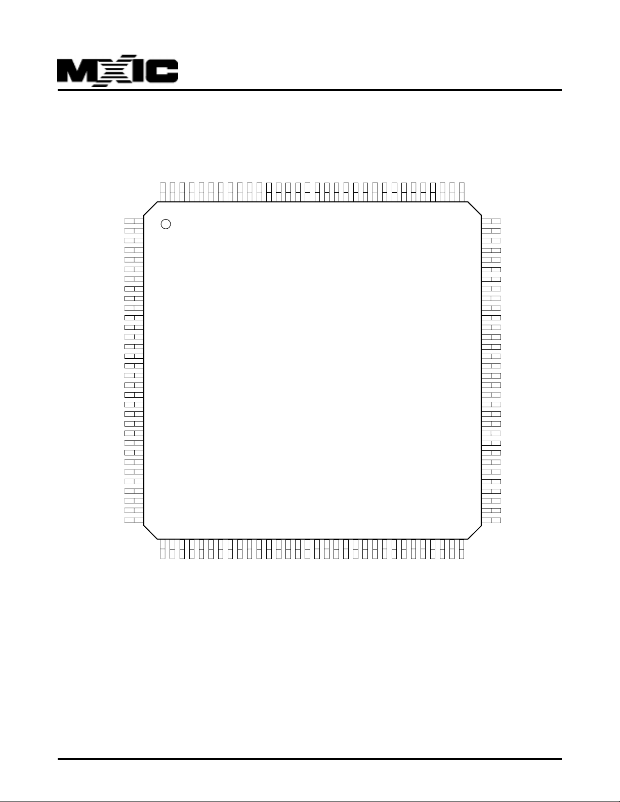
3. PIN CONFIGURATION
HD3
HD11
HD4
HD12
HD5
HD13
HD6
HD14
GNDP
IREQ#
INP ACK#
HD7
HD15
HCE1#
HCE2#
HA10
VCCP
HOE#
IOR#
HA9
GND
IOW#
HA8
VCC
HWE#
HA7
HA6
HA5
HRESET
HA4
MX9691L
WAIT
HA3
FA16
FA15
A14
A13
A12
LED#
GNDP
A11
A10
FA19
FRY/FBY#
INT1#
NMI#
HOLD#
VCCP
WRFLASH0#
WRFLASH1#
FA18
FA17
A15
GNDP
WP#
128
127
126
125
124
123
122
121
120
119
118
117
116
115
114
113
112
111
110
109
108
107
106
105
104
1
2
3
4
5
6
7
8
A9
A8
A7
A6
A5
A4
A3
A2
A1
A0
9
10
11
12
13
14
15
16
17
18
19
20
21
22
23
24
25
26
27
28
29
30
31
32
33343536373839404142434445464748495051525354555657585960616263
MX9691L
103
102
101
100
999897
96
95
94
93
92
91
90
89
88
87
86
85
84
83
82
81
80
79
78
77
76
75
74
73
72
71
70
69
68
67
66
65
64
HA2
REG#
HA1
SPKR
HA0
GNDP
STSCHG
HD0
HD8
HD1
HD9
HD2
HD10
IOIS16#
PWR_RST
TEST
VCCP
X1
X2
GNDP
ROMWR#
ROMCS#
SCTRL#
HLDA#
VCCX32
SWAIT#
NC
GNDX32
DCE#
PCE#
WR#
RD#
P/N:PM0546
D7D6D5D4D3
D2D1D0
GNDP
FCE7#
FCE2#
RDFLASH0#
VCCP
FCE1#
FCE0#
GND
3
FCE6#
FCE5#
FCE4#
FCE3#
VCC
RDFLASH1#
D8
D9
D10
D11
D12
GNDP
D13
D14
D15
SE#
REV. 1.1, JUL. 02, 1999
Page 4

MX9691L
4. PIN DESCRIPTION
Host Interface
Symbol No. Type Description
HA[10:0] 92,94, I Host address line 10-0.
96-97,99 (CMOS) These pins include internal pull-up resistors.
101-103,
106,109,
113
HD[15:0] 84-89, I/O Host data line 15-0.
116-117, (TTL) These pins include internal bus holder circuit that keep
121-128 previous state when tri-state.
HOE#,HWE# 104,111 I Host memory read/write/mode select :
(CMOS) Both pins include internal pull-up resistors that is default in
PCMCIA mode.
IOR#,IOW# 107,110 I Host I/O access.
(CMOS) Both pins include internal pull-up resistor.
HRESET/HRESET# 100 I The host reset signal, when active, initializes the control/
(CMOS) status registers and stops any command in process.
In PCMCIA mode, the signal is active high.
In True IDE mode, this signal is active low.
This signal include internal pull-down resistor.
WAIT/ IOCHRDY 98 O,OD WAIT or INPUT CHANNEL READY : In both PCMCIA and
(CMOS) True IDE modes, this signal holds host transfers until the
controller is ready to respond.
RDY/BSY#/ 119 O, Z READ Y/B USY or HOST INTERR UPT : In PCMCIA mode,
IREQ#/ (CMOS) this signal has two functions. In PCMCIA common memory
HOSTINT mode, this signal is ready/busy. It is asserted busy by the
reset logic, and can be deasserted by the DSP or
represents the ready/busy bit of ATA status register.
In PCMCIA I/O mode, this signal is IREQ#.
In True IDE mode, this active high signal is HOSTINT, which,
when enable, send an interrupt to the host.
P/N:PM0546
REV. 1.1, JUL. 02, 1999
4
Page 5

MX9691L
Symbol No. Type Description
WP/IOCS16# 83 O,OD WRITE PROTECT or 16-bit I/O TRANSFER :
(CMOS) In PCMCIA mode, this bit has two functions. In PCMCIA
common-memory mode,this signal indicates write protect.
In PCMCIA I/O mode, when IOIS16# is asserted low, it
indicates that a 16-bit data transfer is active on PCMCIA
bus.
In True IDE mode, the IOCS16# signal indicates that a
16-bit buffer transf er is activ e on the host b us .
This open drain signal is only driven on assertion(low).
REG#/DA CK# 95 I Attribute memory and I/O select :
(CMOS) In PCMCIA mode, this signal is used to select attribute
memory and I/O space. In T rue IDE mode, this signal is
used during DMA with the DREQ, IOR# and IOW# signals
to transfer data between the host and the MX9691L. This pin
includes an internal pull-up resistor.
HCE1#/ 115 I Card enable 1 or Chip select 0:In PCMCIA mode,this signal
CS1FX# (CMOS) is card enable 1. This signal can enable either even or odd
numbered-address bytes onto HD7:0. In True IDE mode, this
signal accesses the MX9691 command block registers. This
input is ignored during DMA data transfer, i.e. when the
DA CK# signal is low. This pin includes an internal pull-up
resistor.
HCE2#/ 114 I Card enable 2 or Chip select 1:
CS3FX# (CMOS) In PCMCIA mode,this signal is card enable 2. This signal
can enable odd numbered-address bytes onto HD15:8. In
True IDE mode, this signal accesses the MX9691L control
block registers. This pin includes an internal pull-up
resistor.
INPACK#/ DREQ 118 O Input Acknowledge or DMA request :In PCMCIA mode, this
(CMOS) signal is asserted when the MX9691 is configured to respond
to I/O card read cycles at all addresses. In T rue IDE mode,
this signal is DREQ and is issued during DMA transfers to
indicate that the MX9691L is ready for DMA transfer.
SPKR/DASP# 93 I/O Speaker or slave present : In PCMCIA mode, the
(CMOS) output-enable f or this signal is controlled b y the card
configuration registers. In T rue IDE mode, this signal is used
as the slave-present detector .
STSCHG/ 90 I/O Status change or pass diagnostics :In PCMCIA mode, this
PDIAG# (CMOS) signal is used to indicate changes in the RDY/BSY#,WP
signals in card configuration registers. In True IDE mode,
this active low signal is used between two embedded ATA
drive to indicate that the drive in slave mode has passed
diagnostics.
P/N:PM0546
REV. 1.1, JUL. 02, 1999
5
Page 6

MX9691L
External Memory Bus Interface
Symbol No. Type Description
D[15:0] 33-37,39-41, I/O DSP IO/RAM/ROM/FLASH memory array external data bus.
55-58,60-63 (CMOS) These pins include internal pull- up resistors.
A[15:0] 3-5,8-11, I/O In F ree-run mode, these signals are output that used as DSP
22-24,26-31 (CMOS) IO/RAM/ROM e xternal address. A14-A0 are used f or flash
memory array address also. In upgrade mode, these
address are used for ROM address that controlled b y
CYH,CYL registers. In ICE-deb ugging mode,these address
are input, asserted by DSP ICE(external MX93011 DSP).
And the internal DSP is disabled at this time.
These pins include internal pull-up resistors.
PCE# 67 I/O In Free-run mode, this signal is output that is used as
(TTL) external program chip enable. In upgrade mode , this signal
is drived to high. In ICE-deb ugging mode, this signal is
input, asserted by DSP ICE(external MX93011 DSP). And
the internal DSP is disabled at this time. This pin includes a
bus holder circuit.
DCE# 6 8 I/O In Free-run mode, this signal is output that is used as
(TTL) external data chip enable. In upg rade mode, this signal is
drived to high. In ICE-debugging mode , this signal is input,
asserted by DSP ICE(external MX93011 DSP). And the
internal DSP is disabled at this time. This pin includes a bus
holder circuit.
RD# 65 I/O In Free-run mode, this signal is output that is used as DSP
(TTL) IO/RAM/ROM external read. In upgr ade mode, this signal is
output and asserted when the data register is read in host
interface. In ICE-deb ugging mode , this signal is input, as
serted by DSP ICE(external MX93011 DSP). And the
internal DSP is disabled at this time.
This pin includes a bus holder circuit.
WR# 66 I/O In Free-run mode, this signal is output that is used as DSP
(TTL) IO/RAM/ROM external write. In upgrade mode , this signal is
drived to high. In ICE-debugging mode , this signal is input,
asserted by DSP ICE(external MX93011 DSP). And the
internal DSP is disabled at this time. This pin includes a bus
holder circuit.
NMI# 15 I Non maskable interrupt pin.
(CMOS) This pin includes an pull-up resistor .
INT1# 14 I/O In Free-run mode, this signal is input that is used as
(CMOS) interrupt pin. Interrupt will be internally asserted also when
data transfer done, or command end. In ICE-deb ugging
mode, this signal is output and asserted when data transfer
done, or command end. This pin includes an pull-up resistor .
P/N:PM0546
REV. 1.1, JUL. 02, 1999
6
Page 7

MX9691L
Symbol No. Type Description
HOLD# 16 I/O In Free-run mode, this signal is input that is used as holding
(CMOS) DSP clock down and release b us. Bus hold will be internally
asserted also when upgrade mode enable. In ICE-debu g
ging mode, this signal is output and asserted when upgrade
mode enable. This pin includes an pull-up resistor.
HLDA# 73 I/O In Free-run mode, this signal is output that is used as ack to
(CMOS) HOLD# signal. This signal will be internally sent to PCMCIA/
AT A interf ace also when upg rade mode enab le . In ICE-de
bugging mode, this signal is input and ack to HOLD# when
upgrade mode enable.
XF#/SCTRL# 74 O Sleep control, this pin can be directly asserted to low while
(CMOS) power do wn bit is set b y DSP. This pin is connected to
external RC circuit. Def ault inactiv e (Logic High).
In ICE-debugging mode, this signal is used to reset DSP.
Flash Memory Interface
Symbol No. Type Description
F A19/CLE 12 O In linear mode, this signal is used as flash memory chip high
(CMOS) address line 19. In series mode, this signal is used as flash
memory chip command latch enable.
F A18/ALE/ 20 I/O In linear mode, this signal is used as flash memory chip high
ICEMODE (CMOS) address line 18. In series mode, this signal is used as flash
memory chip address latch enable. This signal is also used
to select whether the MX9691 initializes in Free-run mode
or in ICE-debugging mode at power-on reset. If this pin go
high, then the MX9691L will switch to F ree-run mode at
power-on reset,and if this pin remains low , then the MX9691L
will initializes in ICE-debugging mode. This pin includes an
internal pull-up resistor.
ICE-debugging mode select :
ICEMODE=1 —> Free-run mode.
ICEMODE=0 —> ICE-debugging mode.
F A17/ER OM 21 I/O(CMOS) This signal is used as flash memory chip high address line
17. This signal is also used to select whether the firmware
store in linear type flash memory array or in separate
external ROM at power-on reset. If this pin go high, then the
firmware will be executed in linear type flash memory arra y,
and if this pin remains low , then the firmware will be executed
in separate external ROM.
Store firmware in external ROM or linear type Flash memory
array select:
EROM = 0 —> Store in External ROM.
EROM = 1 —> Store in flash memory array.
This pin includes an internal pull-up resistor.
P/N:PM0546
REV. 1.1, JUL. 02, 1999
7
Page 8

MX9691L
Symbol No. Type Description
F A[16:15]/ 1-2 I/O This signal is used as flash memory chip high address line
A TADET[1:0] (CMOS) 16-15. These signals are also used to select configuration in
T rue IDE mode at power-on reset. ATADET1 is connected to
DSP's IPT1. ATADET0 is connected to DSP's IPT0. VDD is
connected to IPT2.
Master/Slave selection in True IDE mode :
AT ADET1 AT ADET0 mode selected
1 1 one driv e
0 0 master of tw o drives
1 0 sla v e of tw o drives
This power-on configuration can be accessed from PCMCIA/
AT A port 601Ch bit3-2. These pins include internal pull-up
resistors.
RDFLASH1# 54 O Flash memory ouptut enable 1 for bank1:
(CMOS) This signal will be asserted by flash memory read operation
when flash memory read address latch, port 601Dh
bit 8= 1(i.e. FA23=1).
Note: Flash memory access window is mapped to 32KW
data and code space 8000h~ffffh.
RDFLASH0# 42 O Flash memory ouptut enable 0 for bank0:
(CMOS) This signal will be asserted by flash memory read operation
when flash memory read address latch, port 601Dh
bit 8 = 0(i.e. FA23=0).
WRFLASH1# 19 O Flash memory write enable 1 for bank1:
(CMOS) This signal will be asserted by flash memory write operation
when flash memory write address latch, port 601Fh
bit 8 = 1(i.e. FA23=1).
WRFLASH0# 18 O Flash memory write enable 0 for bank0:
(CMOS) This signal will be asserted by flash memory write operation
when flash memory write address latch, port 601Fh
bit 8 = 0(i.e. FA23=0).
P/N:PM0546
REV. 1.1, JUL. 02, 1999
8
Page 9

MX9691L
Symbol No. Type Description
FCE[7:0]# 43-44, O Flash memory chip enable 7-0 :
46-47 (CMOS) In linear mode, These signals are decoded from port 601Dh
49-52 bit 7-5 when flash memory read or port 601Fh bit 7-5 when
flash memory write.
Decoding combination :
bit7 bit6 bit5 FCE[7:0]#
0 0 0 11111110
0 0 1 11111011
0 1 0 11101111
0 1 1 10111111
1 0 0 11111101
1 0 1 11110111
1 1 0 11011111
1 1 1 01111111
In series mode, These are decoded from port 601Dh bit 7-5
only when port 601Eh bit 2 is set.
PWD0#/WP# 32 O In linear mode, this signal is used as deep power-down
(CMOS) control of flash memory chips of bank0. PWD0# is activ e
low and also locks out erase or progr am operation providing
data protection during power transitions. P o wer do wn pin
PWD0# will be active if FA23=1.
In series mode, this signal is used to protect the device from
inadvertent programming or erasing. WP# is activ e lo w.
PWD1#/SE# 64 O In linear mode, this signal is used as deep power-down
(CMOS) control of flash memory chips of bank1. PWD1# is activ e
low and also locks out erase or progr am operation providing
data protection during power transitions. P o wer do wn pin
PWD0# will be active if FA23=0. In series mode,this signal
is used to spare area control. SE# is active low.
FRY/FBY# 13 I Flash memory Ready/busy input:
(CMOS) This signal indicate the state of erase or program operation
in flash memory chips.This pin includes an internal pull-up
resistor.
P/N:PM0546
REV. 1.1, JUL. 02, 1999
9
Page 10

MX9691L
Control ROM interface
Symbol No. Type Description
ROMCS#/ 75 O ROM chip select/Flash memory data buffer enable :
FWIN# (CMOS) In Free-run mode, this signal is used as R OM chip enable if
firmware that stored in external ROM. In ICE-deb ugging
mode, this signal is used as flash memory data buffer (74640)
enable if firmware that stored in flash memory array.
ROMWR#/FDIR 76 O ROM write enable/Flash memory data buffer direction
(CMOS) control:
In Free-run mode, this signal is used as ROM write enable if
firmware that stored in external ROM. In ICE-deb ugging
mode, this signal is used as flash memory data buffer (74640)
direction control if firmware that stored in flash memory
array.
Miscellaneous
Symbol No. Type Description
X1 79 I Crystal input.
X2 78 O Crystal ouput.
SWAIT# 71 I(CMOS Sleep wait, this pin is connected to external RC circuit.
Schmitt)
N.C. 70 O No connect.
TEST 81 I This signal is used to select the main system clock, either
(CMOS) from external clock source if this signal is high or from
internal PLL circuit if this signal is low. This pin includes an
internal pull-up resistor.
PWR_RST# 82 I(CMOS Power on reset, CMOS Schmite-triggered:
Schmitt) The MX9691L include debouncing circuit to stabilize
internal DSP reset signal.
LED# 6 O LED output:
(CMOS) This signal is connected to external LED in debugging
system to indicate system status. The LED will be turn-on
during reset. The contorl firmware will turn off the LED after
H/W initialization and pass diagnostics. If system f ail, the
control firmware will flash the LED to indicate some error
occur. This signal will be high if port 601Ch bit0 set to 1 or
OPTR bit2 set to 1.
VCC 17,45,53, 5 or 3.3 volt Power pin
72,80,105,
112
GND 7,25,38, Ground pin
48,59,69,
77,91,108,
120
P/N:PM0546
REV. 1.1, JUL. 02, 1999
10
Page 11
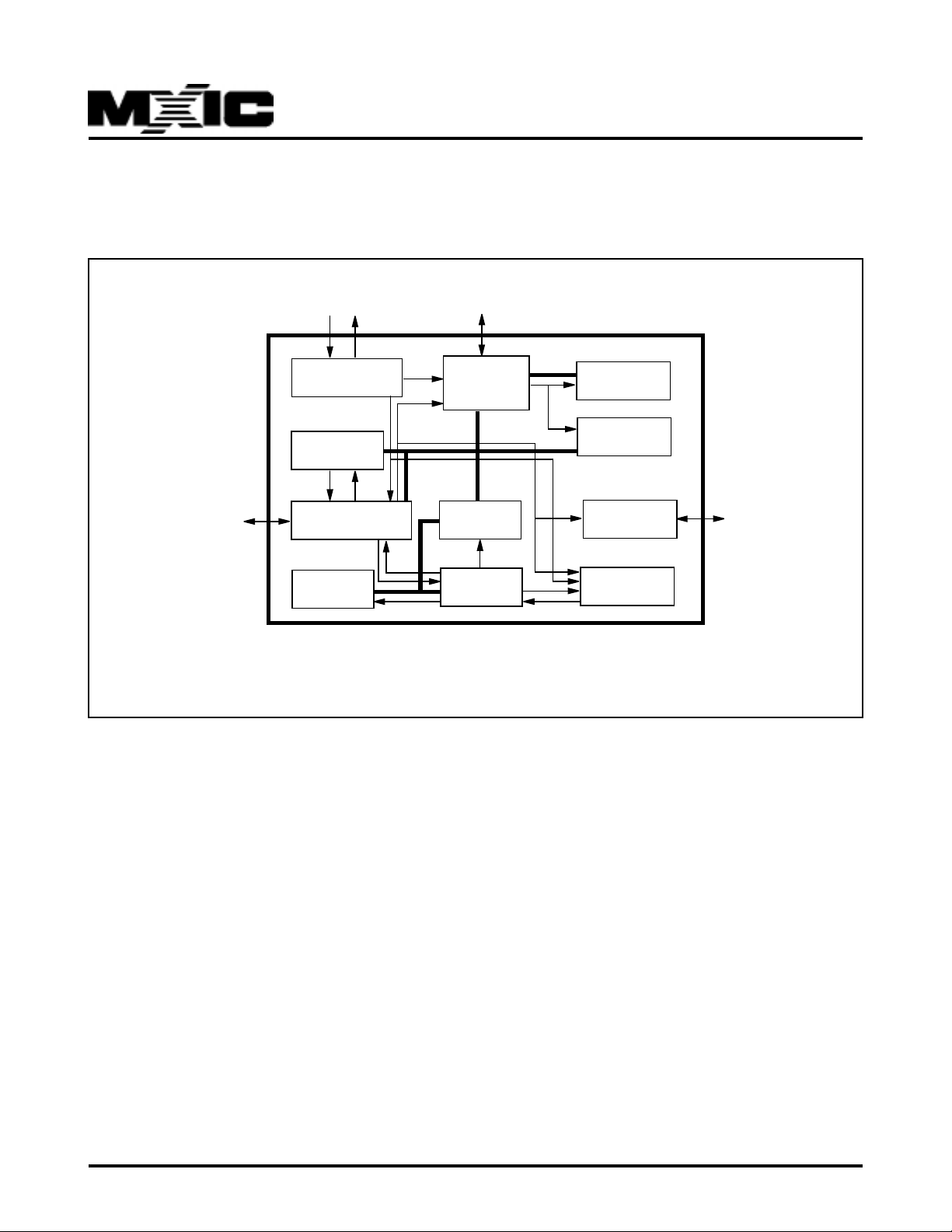
5. Functional and Operation Description
5-1. Block Dia gram
MX9691L
Host Interface
PCMCIA/ATA
Clock
Clock & Reset
Register Bank
PCMCIA/ATA
interface
256 Byte
CIS RAM
External Memory Bus
MX93011
DSP CORE
1KB Buffer
RAM
Buffer RAM
Control
4KB Internal
RAM
2KB Internal
RAM
Flash Memory
Control
ECC Control
Logic
MX9691L Signal Chip Solid State Disk Controller
Flash
Interface
P/N:PM0546
REV. 1.1, JUL. 02, 1999
11
Page 12
5-2. System Memory Map
Data Space :
Address Function & Usage
0000h~007fh Internal RAM (128W) to store control variables
0080h~07ffh Internal RAM(1920W) for flash memory algorithm usage
0800h~5fffh User define (22kW)
6000h~63ffh I/O range(1kW): ATA CTL. use I/O range (6000h~601fh)
6400h~6fffh User define (3kW)
7000h~73ffh User define (1kW)
7400h~77ffh Internal RAM (1kW) for expansion RAM or shadow R OM space
7800h~7fffh ROM Data space(2kW)
8000h~ffffh Flash memory access windows(32kW)
Program Space :
Address Function & Usage
0000h~77ffh ROM program space (32kW)
7800h~7fffh Unused
8000h~ffffh Flash memory access windows(32kW)
MX9691L
5-3. P o wer-on detection
* Store firmware in external ROM or Flash memory array
:
FA17/EROM = 0 —> Store in External ROM
FA17/EROM = 1 —> Store in flash memory array
* Master/Slave selection in True IDE mode :
FA16/ATADET1 FA15/ATADET0 mode selected
1 1 one drive
0 0 master of two drives
1 0 slave of two drives
Note : For some customers design the master/slave
selection is selected by only one jumper that may be
FA16 or FA15. It need to change firmware only.
* ICE debugging mode select :
FA18/ICEMDOE = 0 ---> ICE-debugging mode
FA18/ICEMODE = 1---> Free-run mode, DSP fetch
code from external memory bus and execute it.
* Flash memory data buffer control
ROMCS# is replaced by FWIN# if ICE-debugging
mode & firmware in linear type flash memory array.
ROMWR# is replaced by FDIR if ICE-debugging mode
& firmware in linear type flash memory array.
* PCMCIA mode or True IDE mode select
HOE# Mode
0 True IDE mode
1 PCMCIA mode
To enable True IDE mode this input should be grounded
by the host.
P/N:PM0546
REV. 1.1, JUL. 02, 1999
12
Page 13
MX9691L
5-4. Decoding Configuration of all registers in Host interface
* Common Momory Mode Decode
Register Address Register Read Enable Register Write Enable
CE1# CE2# REG# HA10 HA9:4 HA3:0 HOE# =0 HWE# = 0
0 0 1 0 xh 000xb Read Data Register HD[15:0] Write Data Register HD[15:0]
0 1 1 0 xh 0000b Read Data HD[7:0] Write Data HD[7:0]
Even & Odd byte Even & Odd byte
1 0 1 0 xh 0000b Error Status HD[15:8] Features HD[15:8]
0 1 1 0 xh 0001b Error Status HD[7:0] Features HD[7:0]
1 0 1 0 xh 0001b Error Status HD[15:8] Features HD[15:8]
0 0 1 0 xh 001xb Sector Count HD[7:0] Sector Count HD[7:0]
Sector Number HD[15:8] Sector Number HD[15:8]
0 1 1 0 xh 0010b Sector Count HD[7:0] Sector Count HD[7:0]
0 1 1 0 xh 0011b Sector Number HD[7:0] Sector Number HD[7:0]
1 0 1 0 xh 0011b Sector Number HD[15:8] Sector Number HD[15:8]
0 0 1 0 xh 010xb Cyl. Low HD[7:0] Cyl. Lo w HD[7:0]
Cly. High HD[15:8] Cly. High HD[15:8]
0 1 1 0 xh 0100b Cyl. Low HD[7:0] Cyl. Lo w HD[7:0]
0 1 1 0 xh 0101b Cly. High HD[7:0] Cly . High HD[7:0]
1 0 1 0 xh 0101b Cly. High HD[15:8] Cly. High HD[15:8]
0 0 1 0 xh 011xb Drive/Head HD[7:0] Drive/Head HD[7:0]
Ctl. Status HD[15:8] Command HD[15:8]
0 1 1 0 xh 0110b Drive/Head HD[7:0] Drive/Head HD[7:0]
0 1 1 0 xh 0111b Ctl. Status HD[7:0] Command HD[7:0]
1 0 1 0 xh 0111b Ctl. Status HD[15:8] Command HD[15:8]
0 0 1 0 xh 100xb Read Data Register HD[15:0] Write Data Register HD[15:0]
(Duplicate) (Duplicate)
0 1 1 0 xh 1000b Read Data HD[7:0] Write Data HD[7:0]
Even & Odd byte (Duplicate) Even & Odd byte (Duplicate)
1 0 1 0 xh 1001b Read Data HD[15:8] Write Data HD[15:8]
Odd byte (Duplicate) Odd byte (Duplicate)
0 1 1 0 xh 1001b Read Data HD[7:0] Write Data HD[7:0]
Odd byte (Duplicate) Odd byte (Duplicate)
0 0 1 0 xh 110xb Undefined HD[7:0] Undefined HD[7:0]
Error Status HD[15:8] Features HD[15:8]
(Duplicate) (Duplicate)
0 1 1 0 xh 1101b Error Status HD[7:0] Features HD[7:0]
(Duplicate) (Duplicate)
0 0 1 0 xh 111xb Alternate Ctl. Status HD[7:0] De vice Ctl. HD[7:0]
Drive/Head HD[15:8] Undefined HD[15:8]
0 1 1 0 xh 1110b Alternate Ctl. Status HD[7:0] Device Ctl. HD[7:0]
P/N:PM0546
REV. 1.1, JUL. 02, 1999
13
Page 14

MX9691L
Register Address Register Read Enable Register Write Enable
0 1 1 0 xh 1111b Drive/Head HD[7:0] Not Used
1 0 1 0 xh 1111b Drive/Head HD[15:8] Not Used
0 0 1 1 xh xxxxb Read Data Register HD[15:0] Write Data Register HD[15:0]
0 1 1 1 xh xxx0b Read Data HD[7:0] Write Data HD[7:0]
Even & Odd byte Even & Odd byte
0 1 1 1 xh xxx1b Read Data HD[7:0]Odd b yte Write Data HD[7:0]Odd byte
1 0 1 1 xh xxx0b Read Data HD[15:8] Odd b yte Write Data HD[15:8] Odd byte
1 0 1 1 xh xxx1b Read Data HD[15:8] Odd b yte Write Data HD[15:8] Odd byte
* Independent I/O Mode Decode
Register Address Register Read Enable Register Write Enable
CE1# CE2# REG# HA9:4 HA3:0 IOR# =0 IOW# = 0
0 0 0 xh 0000b Read Data Register HD[15:0] Write Data Register HD[15:0]
0 1 0 xh 0000b Read Data HD[7:0] Write Data HD[7:0]
Even & Odd byte Even & Odd byte
1 0 0 xh 0000b Error Status HD[15:8] Features HD[15:8]
0 1 0 xh 0001b Error Status HD[7:0] Features HD[7:0]
1 0 0 xh 0001b Error Status HD[15:8] Features HD[15:8]
0 1 0 xh 0010b Sector Count HD[7:0] Sector Count HD[7:0]
0 1 0 xh 0011b Sector Number HD[7:0] Sector Number HD[7:0]
1 0 0 xh 0011b Sector Number HD[15:8] Sector Number HD[15:8]
0 1 0 xh 0100b Cyl. Low HD[7:0] Cyl. Low HD[7:0]
0 1 0 xh 0101b Cly . High HD[7:0] Cly. High HD[7:0]
1 0 0 xh 0101b Cly . High HD[15:8] Cly . High HD[15:8]
0 1 0 xh 0110b Drive/Head HD[7:0] Drive/Head HD[7:0]
0 1 0 xh 0111b Ctl. Status HD[7:0] Command HD[7:0]
1 0 0 xh 0111b Ctl. Status HD[15:8] Command HD[15:8]
0 0 0 xh 1000b Read Data Register Write Data Register
HD[15:0](Duplicate) HD[15:0](Duplicate)
0 1 0 xh 1000b Read Data HD[7:0] Write Data HD[7:0]
Even & Odd byte (Duplicate) Even & Odd byte (Duplicate)
1 0 0 xh 1001b Read Data HD[15:8] Write Data HD[15:8]
Odd byte (Duplicate) Odd byte (Duplicate)
0 1 0 xh 1001b Read Data HD[7:0] Write Data HD[7:0]
Odd byte (Duplicate) Odd byte (Duplicate)
0 1 0 xh 1101b Error Status HD[7:0](Duplicate) Features HD[7:0](Duplicate)
0 1 0 xh 1110b Alternate Ctl. Status HD[7:0] Device Ctl. HD[7:0]
0 1 0 xh 1111b Drive/Head HD[7:0] Not Used
1 0 0 xh 1111b Drive/Head HD[15:8] Not Used
P/N:PM0546
REV. 1.1, JUL. 02, 1999
14
Page 15

MX9691L
* Primary A TA Mode Decode
Register Address Register Read Enable Register Write Enable
CE1# CE2# REG# HA9:0 IOR# =0 IOW# = 0
0 0 0 1F0h Read Data Register HD[15:0] Write Data Register HD[15:0]
0 1 0 1F0h Read Data HD[7:0]Even & Odd byte Write Data HD[7:0]Even & Odd byte
1 0 0 1F0h Error Status HD[15:8] Features HD[15:8]
0 1 0 1F1h Error Status HD[7:0] Features HD[7:0]
1 0 0 1F1h Error Status HD[15:8] Features HD[15:8]
0 1 0 1F2h Sector Count HD[7:0] Sector Count HD[7:0]
0 1 0 1F3h Sector Number HD[7:0] Sector Number HD[7:0]
1 0 0 1F3h Sector Number HD[15:8] Sector Number HD[15:8]
0 1 0 1F4h Cyl. Lo w HD[7:0] Cyl. Low HD[7:0]
0 1 0 1F5h Cly. High HD[7:0] Cly . High HD[7:0]
1 0 0 1F5h Cly. High HD[15:8] Cly . High HD[15:8]
0 1 0 1F6h Drive/Head HD[7:0] Drive/Head HD[7:0]
0 1 0 1F7h Ctl. Status HD[7:0] Command HD[7:0]
1 0 0 1F7h Ctl. Status HD[15:8] Command HD[15:8]
0 1 0 3F6h Alternate Ctl. Status HD[7:0] Device Ctl. HD[7:0]
0 1 0 3F7h Drive/Head HD[7:0] Not Used
1 0 0 3F7h Drive/Head HD[15:8] Not Used
* Secondary A TA Mode Decode
Register Address Register Read Enable Register Write Enable
CE1# CE2# REG# HA9:0 IOR# =0 IOW# = 0
0 0 0 170h Read Data Register HD[15:0] Write Data Register HD[15:0]
0 1 0 170h Read Data HD[7:0]Even & Odd byte Write Data HD[7:0]Even & Odd byte
1 0 0 170h Error Status HD[15:8] Features HD[15:8]
0 1 0 171h Error Status HD[7:0] Features HD[7:0]
1 0 0 171h Error Status HD[15:8] Features HD[15:8]
0 1 0 172h Sector Count HD[7:0] Sector Count HD[7:0]
0 1 0 173h Sector Number HD[7:0] Sector Number HD[7:0]
1 0 0 173h Sector Number HD[15:8] Sector Number HD[15:8]
0 1 0 174h Cyl. Low HD[7:0] Cyl. Low HD[7:0]
0 1 0 175h Cly. High HD[7:0] Cly. High HD[7:0]
1 0 0 175h Cly. High HD[15:8] Cly. High HD[15:8]
0 1 0 176h Drive/Head HD[7:0] Drive/Head HD[7:0]
0 1 0 177h Ctl. Status HD[7:0] Command HD[7:0]
1 0 0 177h Ctl. Status HD[15:8] Command HD[15:8]
0 1 0 376h Alternate Ctl. Status HD[7:0] Device Ctl. HD[7:0]
0 1 0 377h Drive/Head HD[7:0] Not Used
1 0 0 377h Drive/Head HD[15:8] Not Used
P/N:PM0546
REV. 1.1, JUL. 02, 1999
15
Page 16

MX9691L
5-5. A utomatic P o wer Sa ving Mode
There are four power saving modes defined in solid state
disk(SSD) system. These four power saving modes are
executed by firmware which use DSP's soft-hold and
power down function and addition logic circuit to implement it.
Active mode : In Active mode the SSD is capable of
ex ecution to file read and write operation.
Idle mode : In Idle mode the SSD polls the events that
include command_in or time_out events. If read/write
command is asserted then the SSD will enter the Active
mode.
Standby mode : The SSD will enter the Standby mode
after time_out(1.25ms) event occurs or standby command is asserted. The SSD controller MX9691L will enter soft_hold condition. The MX9619 will stop program
execution and shut off most circuit activities to sa ve many
Power Saving Flow
power comsumption. The MX9691L will automatically
wake up and enter the Active mode if any command is
asserted.
Sleep mode : The SSD will enter the Sleep mode after
sleep command is asserted. This is most power saving
mode. The SSD controller MX9691L will enter soft _hold
condition and stop main clock and then the all system
activities will stop. This mode can be waked up by H/W
reset, S/W reset or A TA command asserted. The H/W reset will reset all h/w circuits and the Host must reconfigure
the SSD before any command is assseted. The S/W reset will set the busy status until the SSD is ready for accepting command, the Host don't need any h/w
reinitialization. The duration of H/W and S/W reset must
keep enough for main cloc k stabilization.
The A TA command asserted to wake-up latency need the
external RC circuit delay for clock stabilization while the
Solid State Disk(SSD) had entered sleep mode.
H/W Reset
S/W Reset
Power_up
Reset
Initialize
Idle
Standby
Sleep
Command_in
Exit
Time-out1 or standby cmd
Command in
Time-out2 or Sleep cmd
Command in
Active
Wake-up latency
P/N:PM0546
REV. 1.1, JUL. 02, 1999
16
Page 17

MX9691L
5-6. Registers definition
* Registers List
Type of Register Location
PCMCIA/AT A Interface 6000h, 6001h, 6002h, 6003h, 6004h, 6005h, 6006h, 6007h, 600Bh, 6010h,
6011h, 6012h, 6013h, 6019h, 601Ah, 601Bh, 601Ch
PC INTERRUPT CONTROL 6009h, 600Ah
BUFFER MANAGER AND DMA 6008h, 6014h, 6015h, 6016h, 6017h, 6018h
ECC Control 600Ch, 600Dh, 600Eh, 600Fh
Flash Memory Interface 601Dh, 601Eh, 601Fh
* Register Description
Port 6000h :
Bit Function Description
AT CONTROL/STA TUS REGISTER
Default reset value : 01h
7 R/W: DRIVE READY (drive 0)
6 R/W: DRIVE SEEK COMPLETE (drive 0)
5 R/W: CORRECTED D ATA
4 R: ATA INT. ENABLE
3 R: AT SOFTWARE RESET
2 R/W: HOST INTERR UPT
1 R/W: ERROR BIT
0 R/W: BUSY BIT
Port 6001h :
Bit Function Description
Default reset value : 00h
7:0 R/W: ERROR REGISTER (map to command b loc k 1f1h)
Port 6002h :
Bit Function Description
Default reset value : 01h
7:0 R/W: SECT OR COUNT REGISTER (map to command b lock 1f2h)
Port 6003h :
Bit Function Description
Default reset value : 01h
7:0 R/W: SECT OR NUMBER REGISTER (map to command b loc k 1f3h)
P/N:PM0546
17
REV. 1.1, JUL. 02, 1999
Page 18

Port 6004h :
Bit Function Description
Default reset value : 00h
7:0 R/W: CYCLINDER LO W REGISTER (map to command b lock 1f4h)
Port 6005h :
Bit Function Description
Default reset value : 00h
7:0 R/W: CYCLINDER HIGH REGISTER (map to command b lock 1f5h)
Port 6006h :
Bit Function Description
Default reset value : A0h
7:0 R/W: DRIVE/HEAD REGISTER (map to command bloc k 1f6h)
Port 6007h :
Bit Function Description
Default reset value : 00h
7:0 R: COMMAND REGISTER (map to command b lock 1f7h)
MX9691L
Port 6008h :
Bit Function Description
BUFFER RAM SIZE CONTROL REGISTER
Default reset value : 40h
7 R/W: TEST MODE 1 f or HAP/DAP test
0 : DISABLE
1 : ENABLE
6 R/W: BIT WRITE GATE STATE OF DRIVE
0 : ENABLE
1 : DISABLE
5 R: PCMCIA or True IDE mode
0 : True IDE mode
1 : PCMCIA mode
4 R/W: Auto DAP increment
0 : Disable
1 : Enab le
3 R/W: Shadow ROM control
0 : Disable
1 : Enab le
2:0 R/W: BUFFER RAM SIZE CONTR OL
00x : 32KW
010 : 16KW
011 : 8KW
100 : 4KW
101 : 2KW
110 : 1KW
P/N:PM0546
REV. 1.1, JUL. 02, 1999
18
Page 19

111 : 512W
Port 6009h :
Bit Function Description
HOST INTERRUPT STATUS
Default reset v alue : 00h
7 R: Power-Down timer time-out detected
6 R: Card configur ation register write detected
5 R: CIS accessed detected
4 R: Hreset detected
3 R: PC SRST(or PCMCIA SRST) DETECTED
2 R: PC STATUS READ DETECTED
1 R: PC SELECTION
0 R: PC TRANSFER DONE
Port 600Ah :
Bit Function Description
HOST INTERRUPT ENABLE
Default reset v alue : 00h
MX9691L
7 R/W: P ow er-Down timer time-out detected enable .
6 R/W: Card configur ation register write detected enable
5 R/W: CIS accessed detected enab le
4 R/W: Hreset detected enab le
3 R/W: PC SRST(PCMCIA SRST) DETECTED ENABLE
2 R/W: PC STATUS READ DETECTED ENABLE
1 R/W: PC SELECTION ENABLE
0 R/W: PC TRANSFER DONE ENABLE
Port 600Bh :
Bit Function Description
Default reset value : 00h
7:0 R: Feature register (map to command b loc k 1f1h)
P/N:PM0546
REV. 1.1, JUL. 02, 1999
19
Page 20

Port 600Ch :
Bit Function Description
ECC CONTROL REGISTER
Default reset value : 00h
7 R/W: ECC FUNCTION SUSPEND
0 : NORMAL
1 : SUSPEND
6 R/W: CORRECTION SPEED SELECT
0 : FULL SPEED (Max. Clock frequency)
1 : HALF SPEED (1/2 Max. Clock frequency)
5 R/W: ENCODE/DECODE FUNCTION SELECTION
0 : ENCODE
1 : DECODE
4 R/W: RESET ECC CIRCUIT
0 : RESET
1 : NORMAL
3 R: UNCORRECTABLE ERROR FLAG
2 R: CORRECTABLE ERROR FLAG
1 R: CORRECTION DONE FLA G
0 R/W: START ECC CORRECT FUNCTION ENABLE/DISABLE
0 : DISABLE
1 : ENABLE
MX9691L
Port 600Dh :
Bit Function Description
Default reset value : 0000h
15:0 R/W : ECC 0 REGISTER
Port 600Eh :
Bit Function Description
Default reset value : 0000h
15:0 R/W : ECC 1 REGISTER
Port 600Fh :
Bit Function Description
Default reset value : 0000h
15:0 R/W : ECC 2 REGISTER
Port 6010h :
Bit Function Description
Default reset value : 00h
P/N:PM0546
REV. 1.1, JUL. 02, 1999
20
Page 21

7:0 R: Configuration Option register (map to attribute memory 200h)
Port 6011h :
Bit Function Description
Default reset v alue : 00h
7:0 R: Card Configuration and status register (map to attribute memory 202h)
Port 6012h :
Bit Function Description
Default reset value : 0Ch
7:0 R: Pin replacement register (map to attribute memory 204h)
Port 6013h :
Bit Function Description
Default reset value : 00h
7:0 R: Sock et and copy register (map to attribute memory 206h)
Port 6014h :
Bit Function Description
Default reset value : 0000h
15:0 R/W : HOST ADDRESS POINTER
MX9691L
Port 6015h :
Bit Function Description
Default reset value : 00ffh
15:0 R/W : AT STOP POINTER
Port 6016h :
Bit Function Description
Default reset value : 0000h
15:0 R/W : DISK ADDRESS POINTER
Port 6017h :
Bit Function Description
DMA CONTROL REGISTER
Default reset value : 08h
7 R/W: DRIVE READY (drive 1)
6 R/W: DRIVE SEEK COMPLETE (drive 1)
5 R/W: set BSY upon XFER done
0 : DISABLE
1 : ENABLE
4 R/W: ENABLE AUTO INTERRUPTS - AT ONLY
0 : DISABLE
P/N:PM0546
REV. 1.1, JUL. 02, 1999
21
Page 22

1 : ENABLE
Port6017h:
Bit Function Description
3 R/W: BUFFER RAM CHIP ENABLE
0 : ENABLE
1 : DISABLE
2 R/W: HOST BUS DIRECTION
0 : START BUFFER ---> AT BUS
1 : START AT BUS ---> BUFFER WHEN SET
1 R: A COMPLETION OF AT DMA XFER
0 R/W: START D ATA TRANSFER BETWEEN AT BUS AND BUFFER RAM
0 : DISABLE
1 : ENABLE
Port 6018h :
Bit Function Description
15:0 R/W : ACCESS POR T INTO BUFFER RAM
MX9691L
Port 6019h :
Bit Function Description
PCMCIA control register
7 R: True IDE mode
6 R: Common memory mode
5 R: I/O mode
4 R/W: host ready
3 R/W: no drive address
2 R/W: Internal registers write pulse width
0 : 2 system clock
1 : 1 system clock
1 R/W: Reserved.
P/N:PM0546
REV. 1.1, JUL. 02, 1999
22
Page 23

0 R/W: Reserved.
Port 601Ah :
Bit Function Description
Auxi_ctl_1 reg.
Default reset v alue : 00h
7 R/W : DASP
6 R/W : Host Interrupt le v el mode or pulse mode select
0: Le v el mode
1: Pulse mode
5 R/W : PDIAG
4 R/W : DASP output enable
3 R/W: write protect enable
0: Disab le
1: Enab le
2 R/W: PDIA G output enable
1 R/W: master/slav e mode enable
0: Disable
1: Enab le
0 R/W: master/salve of T rue IDE mode
0: master
1: slave
MX9691L
Port 601Bh :
Bit Function Description
Auxi_ctl_2 reg.
Default reset v alue : 00h
7:4 Reserved.
3 R/W: Reserved.
2 R/W: Deep po w er down control f or automatic w ak e-up function from sleep mode.
0 : Disab le
1 : Enab le
1 R/W: Reserved.
0 R/W: Disk interrupt polarity
0: Low active
P/N:PM0546
23
REV. 1.1, JUL. 02, 1999
Page 24

1: High activ e
Port 601Ch :
Bit Function Description
Auxi_ctl_3 reg.
Default reset value : 0000h
15 Reserved.
14 R/W : Test mode 2 for timer
0 : Normal mode
1 : T est mode enab le
13 R : DRQ
12 R : Time out status
1 : Time out event occurence
11 R/W: Timer enable/disable
0 : Disable
1 : Enab le
10:9 R/W: Po wer-do wn timer time-out select f or 25MHz main cloc k
00 : 16 x 1.28 = 20.48 sec.
01 : 8 x 1.28 = 10.24 sec.
10 : 4 x 1.28 = 5.12 sec.
11 : 2 x 1.28 = 2.56 sec.
8 R : ICE-debugging mode detected
0 : ICE-deb ugging mode
1 : Free-run mode.
7 R/W : Inverted data bus for access flash memory .
0 : In v erted.
1 : Non-in verted.
6 R: External ROM detect.
0: Firmware stored in external ROM.
1: Firmware stored in linear type flash memory array.
5:4 R/W: Shadow R OM space control
00 : 512 b ytes, Range: 7400h ~ 74ffh
01 : 1Kb ytes, Range: 7400h ~ 75ffh
10 : 1.5Kbytes , Range: 7400h ~ 76ffh
11 : 2Kb ytes, Range: 7400h ~ 77ffh
3:2 R : Master/Sla v e mode detect in T rue IDE mode
00 : Master of tw o drives
10 : Sla ve of two drives
11 : One drive
1 R/W: PIO/DMA mode select
0: PIO mode.
MX9691L
P/N:PM0546
REV. 1.1, JUL. 02, 1999
24
Page 25

MX9691L
1: DMA mode.
0 R/W: LED output
Port 601Dh :
Bit Function Description
Default reset value : 0000h
9:0 R/W : Flash memory Read address FA[24:15] latch in linear mode When data space 8000h ~ ffffh is
read, the output of the flash memory read address latch will be used.
The definitions for this register in series mode
Default reset value : 0000h
9 Reserved.
8 Bank select in capacity extension mode
0 : Bank0 selected.
1 : Bank1 selected.
7:5 R/W: FCE select for series mode
000: FCE0
001: FCE2
010: FCE4
011: FCE6
100: FCE1
101: FCE3
110: FCE5
111: FCE7
4 R/W: Command latch enab le (FA19/CLE)
0 : Disab le
1 : Enab le
3 R/W: Address latch enab le (FA18/ALE)
0 : Disab le
1 : Enab le
2:0 Reserved
Port 601Eh :
Bit Function Description
Flash memory control register
Default reset value : 08Ah
7 R/W: Flash memory deep power down control 0 in linear mode or Write protect in series mode
0 : Enab le
1 : Disable
6 R : Ready / Busy status
P/N:PM0546
25
REV. 1.1, JUL. 02, 1999
Page 26

MX9691L
0 : BUSY
1 : READY
Port 601Eh :
Bit Function Description
5:4 R/W: Flash memory type select
00 : Reserved.
01 : 16M flash memory /Bank 1 select in linear mode or capacity extension mode selected in series
mode.
10 : Reserved
11 : Reserved
3 R/W: Flash memory deep power down control 1 in linear mode or Spare area enab le in series mode.
0 : Enab le
1 : Disable
2 R/W: CE# enable f or series mode
0 : Disable
1 : Enab le
1 R/W: Series or linear mode select
0 : linear mode
1 : Series mode
0 R/W: Flash memory write pulse width control
0 : 1 system clock
1 : 2 system clock
Port 601Fh :
Bit Function Description
Default reset value : 0000h
9 R/W : Flash memory Write address FA[24:15] latch in linear mode
When data space 8000h ~ ffffh is write or program space 8000h ~ ffffh is read, the output of the flash
memory write address latch will be used.
The definitions for this register in series mode
Reserved.
8 Bank select in capacity extension mode
0 : Bank0 selected.
1 : Bank1 selected.
7:0 Reserved.
P/N:PM0546
REV. 1.1, JUL. 02, 1999
26
Page 27

6. ELECTRICAL SPECIFICATIONS
MX9691L
6-1. DC Characteristics 1 : Ta = 0 oC to 70 oC, VCC = 5V
Symbol Parameter Min Max Units Conditions
VCC Pow er Supply voltage 4.5 5.5 V
VIL1 Input Low voltage (TTL) 0.8 V VCC=5V
VIH1 Input High voltage (TTL) 2.0 V VCC=5V
VIL2 Input Low voltage (CMOS) 1.2 V VCC=5V
VIH2 Input High voltage (CMOS) 3.5 V VCC=5V
VOL Output Low voltage 0.4 V IOL=8mA
VOH Output High voltage 2.5 V IOH=-8mA
ICC1 Supply Current 1 40 m A f=25Mhz, Active mode , CL=0pf ,
ICC2 Supply Current 2 30 mA f = 25Mhz, Idle mode, CL = 0pf,
ICC3 Supply Currect 3 12 mA f = 25Mhz, Standby mode, CL = 0pf ,
ICC4 Supply Current 4 1 mA f = 0Mhz, Sleep mode, CL = 0pf,
IL Input Leakage ±1 0 uA 0< VIN < VCC
CIN Input Capacitance 14 pf VIN=0V
COUT Output Capacitance 16 pf VOUT=0V
±±
±10%
±±
VCC=5.5V olt, T emperature= 0oC
VCC=5.5V olt, T emperature= 0oC
VCC=5.5V olt, T emperature= 0oC
VCC=5.5V olt, T emperature= 0oC
Note : During transitions, inputs ma y undershoot to -2.0V for periods less than 20ns and overshoot to VCC + 2.0V for
periods less than 20ns.
P/N:PM0546
27
REV. 1.1, JUL. 02, 1999
Page 28

MX9691L
6-2. DC Characteristics 2 : Ta = 0 oC to 70 oC, VCC = 3.3V
Symbol Parameter Min Max Units Conditions
VCC Pow er Supply voltage 3.1 3.5 V
VIL1 Input Low voltage(TTL) 0.8 V VCC=3.3V
VIH1 Input High voltage(TTL) 2.0 V VCC=3.3V
VIL2 Input Low voltage(CMOS) 0.9 V VCC=3.3V
VIH2 Input High voltage(CMOS) 2.7 V VCC=3.3V
VOL Output Low voltage 0.4 V IOL=4mA
VOH Output High voltage 2.2 V IOH=-4mA
ICC1 Supply Current 1 20 mA f=16Mhz, Active mode, CL=0pf ,
ICC2 Supply Current 2 15 mA f = 16Mhz, Idle mode, CL = 0pf,
ICC3 Supply Currect 3 5 mA f = 16Mhz, Standby mode, CL = 0pf,
ICC4 Supply Current 4 0.5 mA f = 0Mhz, Sleep mode, CL = 0pf,
IL Input Leakage ±1 0 uA 0< VIN < VCC
CIN Input Capacitance 14 pf VIN=0V
COUT Output Capacitance 16 pf VOUT=0V
±±
±5%
±±
VCC=3.5V olt, T emperature= 0oC
CC=3.5V olt, T emperature= 0oC
VCC=3.5V olt, T emperature= 0oC
VCC=3.5V olt, T emperature= 0oC
Note : During transitions, inputs ma y undershoot to -2.0V for periods less than 20ns and overshoot to VCC + 2.0V f or
periods less than 20ns.
P/N:PM0546
REV. 1.1, JUL. 02, 1999
28
Page 29

MX9691L
6-3. A C Characteristics
Condition : Ta=0 oC to 70 oC, VCC = 5V±10% or VCC = 3.3V±5%
(1). DSP Interface Timing :
VCC = 5V±10%
Symbol Description Min. Typ. Max. Units
Tw In ICE mode, WR# pulse duration when the data are 4Tc
accessed by external DSP.
Trd In ICE mode, RD# to output delay when the data are 34 ns
accessed by external DSP.
Tcs Chip select access cycle 1.5Tc 4.5Tc ns
Taa Address access cycle 1.5Tc 4.5Tc ns
Trds Data setup time before RD# high 12 ns
Tdh Data hold time after RD# high 0 ns
VCC = 3.3V±5%
Symbol Description Min. Typ. Max. Units
Tw In ICE mode, WR# pulse duration when the data are 4Tc
accessed by external DSP.
Trd In ICE mode, RD# to output delay when the data are 34 ns
accessed by external DSP.
Tcs Chip select access cycle 1.5Tc 4.5Tc ns
Taa Address access cycle 1.5Tc 4.5Tc ns
Trds Data setup time before RD# high ns
Tdh Data hold time after RD# high ns
P/N:PM0546
REV. 1.1, JUL. 02, 1999
29
Page 30

A[15:0]
DCE#
MX9691L
WR#
D[15:0]
A[15:0]
DCE#
RD#
D[15:0]
DCE#/PCE#
Tw
Trd
Tcs
P/N:PM0546
A[15:0]
RD#
D[15:0]
30
Taa
Trds
Tdh
REV. 1.1, JUL. 02, 1999
Page 31

MX9691L
(2). P o wer Reset Timing
VCC = 5V±10% or VCC = 3.3V±5%
Symbol Description Min. Typ. Max. Units
Tw(rst) Reset low pulse width 3Tc ns
(3). Clock Timing
VCC = 5V±10%
Symbol Description Min. Typ. Max. Units
Tc(c) Clock cycle time 40 ns
Tlpd(c) Clock low pulse duration(Tc=40ns) 16 24 ns
Thpd(c) Clock high pulse duration(Tc=40ns) 16 24 ns
VCC = 3.3V±5%
Symbol Description Min. Typ. Max. Units
Tc(c) Clock cycle time 62.5 ns
Tlpd(c) Clock low pulse duration(Tc=62.5ns) 25 37.5 ns
Thpd(c) Clock high pulse duration(Tc=62.5ns) 25 37.5 ns
CLK IN
PWR RST#
TlpdThp
Tc
Tw(rst)
P/N:PM0546
REV. 1.1, JUL. 02, 1999
31
Page 32

MX9691L
(4). Interrupt Timing
VCC = 5V±10%
Symbol Description Min. Typ. Max. Units
Tw INT1# low pulse duration 1.5Tc ns
Tf INT1# fall time 10 ns
VCC = 3.3V±5%
Symbol Description Min. Typ. Max. Units
Tw INT1# low pulse duration 1.5Tc ns
Tf INT1# fall time ns
(5). HOLD# Timing
VCC = 5V±10% or VCC = 3.3V±5%
Symbol Description Min. Typ. Max. Units
Td(al-h) HLD A# lo w to address tri-state 0 ns
Td(hh-ha) HOLD# high to HLDA# high 0 0.5Tc 0.5Tc+10 ns
Ten(ah-a) Address driven after HLDA# high 0.5Tc-10 0.5Tc Tc ns
INT1
HOLD#
HLDA#
A[15:0]
Tf
Tw
Td(hh-ha)
Td(al-h)
Ten(ah-a)
P/N:PM0546
REV. 1.1, JUL. 02, 1999
32
Page 33

MX9691L
(6). PCMCIA Bus Timing 1: Common Memory and Attribute memory Access Timing
VCC = 5V±10%
Symbol Parameter Min (ns) Max (ns)
T1 Read cycle time 60
T2 Chip enable setup time before output enable 0
T3 Output data enable time from HOE# 31
T4 Chip disable hold time following output disable 1.5
T5 Output data disable time following HOE# 10.5
T6 Write cycle time 60
T7 Chip enable setup time before HWE# 0
T8 Write pulse width of HWE# 40
T9 Chip disable hold time following write disable 2
T10 Data setup time before HWE# 0
T11 Data hold time following HWE# 2.5
VCC = 3.3V± 5%
Symbol Parameter Min (ns) Max (ns)
T1 Read cycle time 90
T2 Chip enable setup time before output enable 0
T3 Output data enable time from HOE# 47
T4 Chip disable hold time following output disable 3
T5 Output data disable time following HOE# 17
T6 Write cycle time 90
T7 Chip enable setup time before HWE# 0
T8 Write pulse width of HWE# 60
T9 Chip disable hold time following write disable 2.5
T10 Data setup time before HWE# 0
T11 Data hold time following HWE# 3
P/N:PM0546
REV. 1.1, JUL. 02, 1999
33
Page 34

Common Memory and Attribute Memory Read Timing
T1
HA[10:0]
REG#
CE[2:1]#
MX9691L
T2
HOE#
HD[15:0]
T3
Common Memory and Attribute Memory WriteTiming
T6
HA[10:0]
REG#
CE[2:1]#
T7
HWE#
HD[15:0]
T8
T4
T5
T9
T11
P/N:PM0546
T10
REV. 1.1, JUL. 02, 1999
34
Page 35

MX9691L
(7). PCMCIA Bus Timing 2: I/O mode Access Timing
VCC = 5V±10%
Symbol Parameter Min (ns) Max (ns)
T1 Address hold time following IOR# 2
T2 REG# setup time before IOR# 0
T3 REG# hold time following IOR# 0
T4 CE# setup time before IOR# 0
T5 IOR# pulse width 60
T6 CE# hold time following IOR# 2
T7 Address setup time before IOR# 0
T8 INPA CK dela y from IOR# falling edge 10
T9 INPA CK delay from IOR# rising edge 10.5
T10 IOIS16 falling delay after Address changed 14
T11 Data delay after IOR# falling 32
T12 IOIS16 rising delay after Address changed 12.5
T13 Data hold time following IOR# 20
T14 Address hold time following IOW# 3
T15 REG# setup time before IOW# 0
T16 REG# hold time following IOW# 0
T17 CE# setup time before IOW# 0
T18 IOW# pulse with 60
T19 CE# hold time following IOW# 2
T20 Address setup time before IOW# 0
T21 IOIS16 rising delay after Address changed 10.5
T22 IOIS16 falling delay after Address changed 14
T23 Data setup time before IOW# 0
T24 Data hold time following IOW# 2.5
P/N:PM0546
REV. 1.1, JUL. 02, 1999
35
Page 36

MX9691L
VCC = 3.3V±5%
Symbol Parameter Min (ns) Max (ns)
T1 Address hold time following IOR# 2
T2 REG# setup time before IOR# 0
T3 REG# hold time following IOR# 0
T4 CE# setup time before IOR# 0
T5 IOR# pulse width 90
T6 CE# hold time following IOR# 2
T7 Address setup time before IOR# 0
T8 INPA CK dela y from IOR# falling edge 18
T9 INPA CK delay from IOR# rising edge 18
T10 IOIS16 falling delay after Address changed 23.5
T11 Data delay after IOR# falling 47
T12 IOIS16 rising delay after Address changed 20
T13 Data hold time following IOR# 31
T14 Address hold time following IOW# 4
T15 REG# setup time before IOW# 0
T16 REG# hold time following IOW# 0
T17 CE# setup time before IOW# 0
T18 IOW# pulse with 90
T19 CE# hold time following IOW# 2.5
T20 Address setup time before IOW# 0
T21 IOIS16 rising delay after Address changed 20
T22 IOIS16 falling delay after Address changed 23.5
T23 Data setup time before IOW# 0
T24 Data hold time following IOW# 3
P/N:PM0546
REV. 1.1, JUL. 02, 1999
36
Page 37

ID Read Timing
HA[10:0]
REG#
CE[2:1]#
IOR#
T2
T4
MX9691L
T1
T3
T6
T5
INPACK#
IOIS16#
HD[15:0]
I/O Write Timing
HA[10:0]
REG#
CE[2:1]#
IOW#
IOIS16#
T10
T7
T20
T15
T17
T8
T11
T9
T12
T13
T14
T16
T19
T18
T21
P/N:PM0546
HD[15:0]
T22
T23
T24
REV. 1.1, JUL. 02, 1999
37
Page 38

MX9691L
(8). Flash Memory Interface Timing
VCC = 5V±10%
Symbol Parameter Min Max Units
Tw(a-ce) FCE# fall time after DSP address decode when write 5.5 15 ns
Twas FCE# setup time before WRFLASH# falling edge 10 29.5 ns
Tw(wrflash) WRFLASH# low pulse duration 1Tc
Tr(a-ce) FCE# fall time after DSP address decode when read 5.5 15 ns
Tr(rd-oe) RDFLASH# fall time after RD# f alling edge 4.5 11.5 ns
VCC = 3.3V±5%
Symbol Parameter Min Max Units
Tw(a-ce) FCE# fall time after DSP address decode when write 8 24.5 ns
Twas FCE# setup time before WRFLASH# falling edge 14.5 49 ns
Tw(wrflash) WRFLASH# low pulse duration 1Tc
Tr(a-ce) FCE# fall time after DSP address decode when read 8 24.5 ns
Tr(rd-oe) RDFLASH# fall time after RD# f alling edge 6.5 20 ns
[* Note]: Theses timing are only for 1-system cloc k of flash memory write pulse is employed (601E[0]=0). If 2-system
clock of pulse width is selected (601E[0]=1), the minimum time of Tw(wrflash) is 2Tc.
*
*
ns
ns
Flash memory write timing
A[15:0]
FCE[7:0]
WR#
WRFLASH#
Flash memory Read timing
A[15:0]
FCE[7:0]
RD#
Tw(a-ce)
Twas
Tw(wrflash)
Tr(a-ce)
Tras
P/N:PM0546
RDFLASH#
REV. 1.1, JUL. 02, 1999
38
Page 39

6-4. Latchup Characteristics
Min. Max.
Input Voltage with respect to GND on all VCC pins -2.0V 12.0V
Input Voltage with respect to GND on all I/O pins -2.0V VCC+2.0V
Current -100mA +100mA
Includes all pins expect GND. Test conditions:VCC=5.0V, one pin at a time.
MX9691L
P/N:PM0546
REV. 1.1, JUL. 02, 1999
39
Page 40

MX9691L
REVISION HISTOR Y
Revision Destription Pa ge Date
1.1 Modify package type P1 JUL/02/1999
P/N:PM0546
REV. 1.1, JUL. 02, 1999
40
Page 41

MX9691L
MACRONIX INTERNATIONAL CO., LTD.
HEADQUARTERS:
TEL:+886-3-578-6688
FAX:+886-3-563-2888
EUROPE OFFICE:
TEL:+32-2-456-8020
FAX:+32-2-456-8021
JAPAN OFFICE:
TEL:+81-44-246-9100
FAX:+81-44-246-9105
SINGAPORE OFFICE:
TEL:+65-348-8385
FAX:+65-348-8096
TAIPEI OFFICE:
TEL:+886-2-509-3300
FAX:+886-2-509-2200
MACRONIX AMERICA, INC.
TEL:+1-408-453-8088
FAX:+1-408-453-8488
CHICAGO OFFICE:
TEL:+1-847-963-1900
FAX:+1-847-963-1909
http : //www.macronix.com
MACRONIX INTERNATIONAL CO., LTD. reserves the right to change product and specifications without notice.
41
 Loading...