

Page 1
MX9 3002
1 Ver 2.50 September 17, 1998
FEATURES
. Built-in two single +5V power supply PCM CODECs
. Support Digital Speakerphone application
. Support automatic power-down function
. Support 2.048 or 1.536 MHz master clock for 8KHz
Frame Sync.
. Support £g/A law and 16-bit format linear data
. Support switch paths for DAM (digital answering
machine) related applications
. Support two comparators for power-low and
battery- low detection
7. Support external L.P.F. for D/A output path
. Support external volume control
. On-chip differential line driver
. On-chip ALC (automatic level control)
. On-chip digital volume control
. On-chip differential 8Ω power amplifier
. On-chip programmable receive/transmit gain
control
. Easy interface to general purpose DSP
. Easy Read/Write of control registers by MCU
. Easy interface to FAX or Cordless Phone
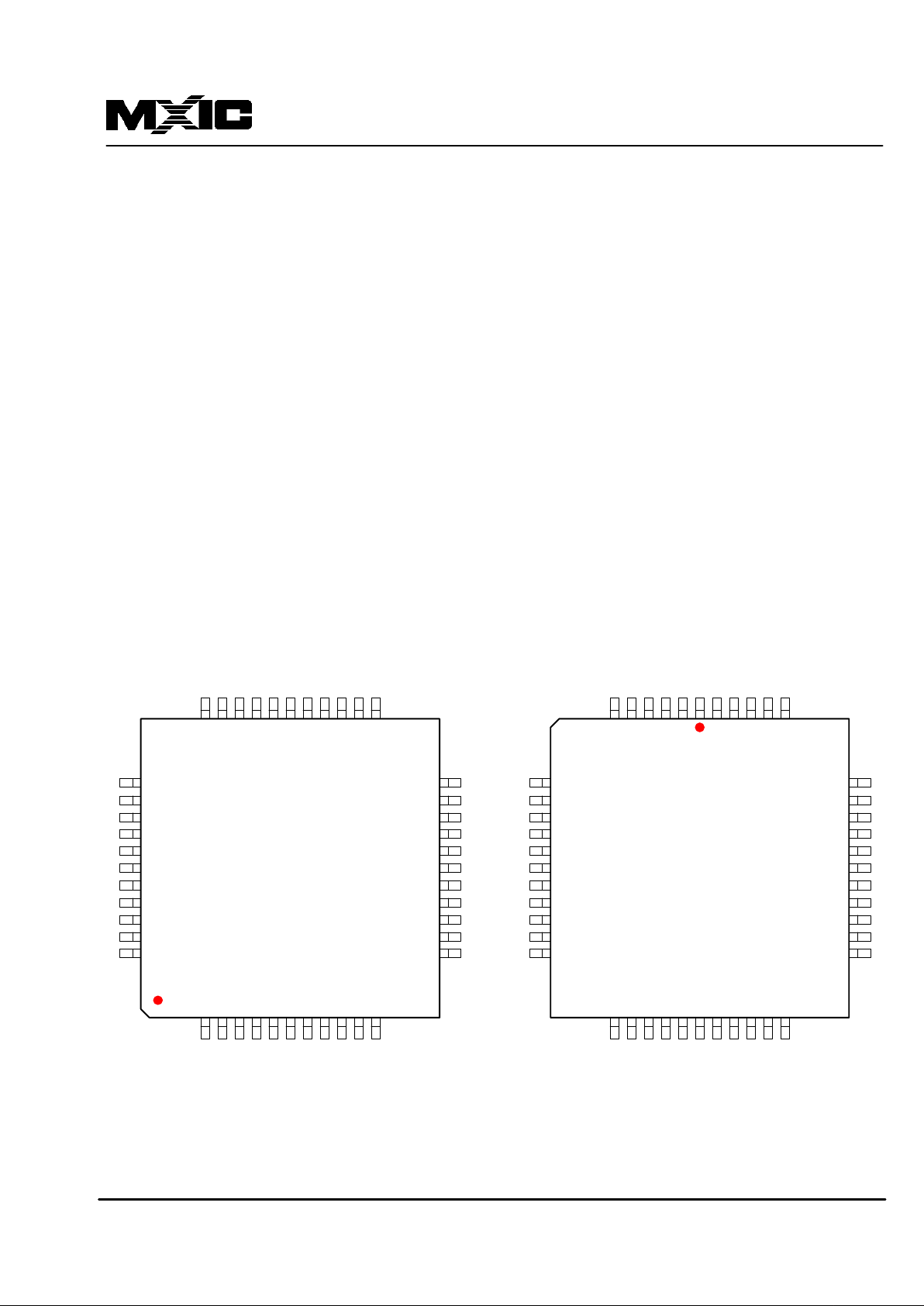
. 44-pin PQFP/PLCC package
PIN CONFIGURATION
44 PINS PQFP
1 2 3 4 5 6 7 8 9 101
1
12
13
14
16
17
18
19
20
21
22
232425262728293031323
3
34
35
37
38
39
40
41
42
43
44
15
36
44 PINS PLCC
181
9
272
8
29
30
31
33
35
36
37
38
39
404142434
4123456
8
10
11
13
14
15
16
17
32
9
7
12
2021222324252
6
34
DGND
VDD
MCLK
FS
DR1
DX1
SDATA
S
D
E
N
B
FILT
S
V
D
D
1
S
V
D
D
2
S
P
K
N
S
G
N
D
S
P
K
P
A
U
X
2
VRL
P
F
C
2
L
P
F
C
1
ALCC2
ALCC1
ALCRC
PGAC1
AUX1
LIN
VREF
AG
VBG
A
V
D
D
L
O
U
T
N
L
O
U
T
P
V
B
A
T
B
A
T
B
V
P
O
W
P
O
W
B
SCLK
MIC
C
P
P
V
D
D
A
G
N
D
PGND
DR2
DX2
V
C
O
M
P
DGND
VDD
MCLK
FS
DR1
DX1
SDATA
S
D
E
N
B
FILT
S
V
D
D
1
S
V
D
D
2
S
P
K
N
S
G
N
D
S
P
K
P
A
U
X
2
VRL
P
F
C
2
L
P
F
C
1
ALCC2
ALCC1
ALCRC
PGAC1
AUX1
LIN
VREF
AG
VBG
A
V
D
D
L
O
U
T
N
L
O
U
T
P
V
B
A
T
B
A
T
B
V
P
O
W
P
O
W
B
SCLK
MIC
C
P
P
V
D
D
A
G
N
D
P
G
A
C
2
PGND
DR2
DX2
V
C
O
M
P
P
G
A
C
2
Page 2

MX9 3002
2
PRODUCT OVERVIEW
The MX93002 PCM CODEC integrates key functions of the analog-front-end of DAM (with Digital Speakerphone)
related products into an integrated circuit. The MX93002 PCM CODEC is especially powerful when applied to some
DAM models which are intended to meet different countries' specifications in the same system hardware. User
can achieve this goal by simply setting control firmware. This benefit will help DAM system makers to save
developing time and R&D resources.
The MX93002 has two A/D, D/A converters so as to meet the requirement of the digital speakerphone application.
The on-chip digital filters, which are carried out with 16-bit and 2's complement format, are used to get required
frequency response of a PCM CODEC. The CODEC can support 8-bit u/A law and linear data format. For the latter,
it is 16-bit format with 14-bit resolution.
Before the A/D digitizing the voice-band analog signal into digital format, the analog signal can be processed by a
built-in Automatic Level Control (
ALC
) and PRE-Programmable Gain Amplifier (
PRE-PGA
). The
ALC
circuit
controls the signal level about 1.2Vpp and
AD1-PGA
can provide 0 ~ 18dB gain to get more larger signal. The
PRE-PGA
circuit is used to control the gain of different sources like
MIC, AUX1
or
LIN
input.
After the digital data is converted into analog signal by D/A converter, a fully differential line driver and speaker
driver are supported to drive the telephone line and 8Ω speaker directly without needing any external amplifiers.
Besides, the analog signal can be monitored by passing the on-chip volume control or external volume control.
The MX93002 supports many switches as well. User can program the control registers of the PCM CODEC to
accomplish all specific operations of DAM (with digital speakerphone function) related products.
In order to let MCU (Micro controller) easily Read/Write the control registers of the MX93002, the sampling clock of
the serial control data is clocked by external
SCLK
clock and synchronized by
SDENB
, where
SDENB
signal is
coming from the MCU output port by detecting one of the rising edge of external
SCLK
clock.
Page 3
MX9 3002
3
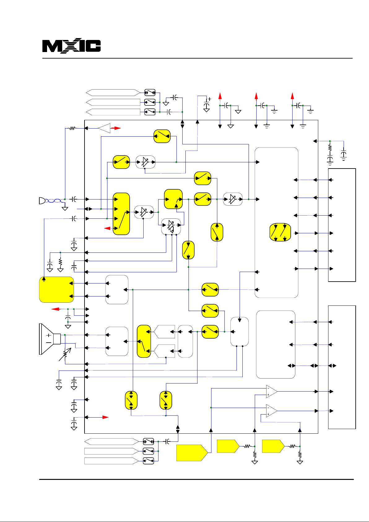
BLOCK DIAGRAM ( PQFP )
AIN1
2 PCM CODECS
FILT
POWB
BATB
VBATVPOW
4
6
22
R6
R7
AVDD
10
AVDD
AGND
SERIAL
CONTROL
UNIT
R4
R5
75
VBG
AG
13
AG
24
LPFC1
25
LPFC2
11
C5
C14C13
C16
C7
VREF
15
R2
14
C8
MIC
AG
17
16
ALCC2
ALCC1
21
19
20
18
+
R3
ALCRC
C9
C11
C10
FAX TXA
Corelessphone TXA
AUX-I/O
SWE
SWK
LOUTN
8
9
LIN
DRV
TELEPHONE
LINE
INTERFACE
LOUTP
SWF
VR
27
SPK
29
31
VR1
AOUT2
SWH
FAX RXA
Corelessphone RXA
AUX-I/O
AUX2
26
12
C15
43
C4
42
VDD
33
34
SDENB
SDATA
35
SCLK
uP
check
SYSTEM
Battery
uP
check
SYSTEM
Power
uP
TX / RX
Control
DATA
uP
Enable
SDATA
uP
Send
SCLK
C12
SVDD1
SVDD2
SGND
28
32
30
AVDD
MIC
A
c
a
b
AG
d
AUX1
LIN
SWA
PGAC1
SWD
b
A
SWC
a
SWI
L.P.F.
DGNDAGND
DGND
SWL
POW
BAT
SWM
ALC
PRE
PGA
AD1
PGA
C6
AD2
PGA
23
PGAC2
SWJ
AOUT1
AIN2
DSP
Receive
DATA1
DSP
Transmit
DATA1
DSP
Frame
Sync.
signal
DSP
Master
Clock
signal
DSP
Receive
DATA2
DSP
Transmit
DATA2
41
37
36
40
MCLK
FS
DR1
DX1
39
38
DR2
DX2
SWB
A
I
N
1
A
O
U
T
1
A
O
U
T
2
A
I
N
2
VCOMP
3
1
CP
C1
R1
C2
AC/DC
ADAPTOR
BATTERY
POWER
V reference
for POW and BAT
2 Comparators
VDD
44
C3
2
PVDD
DGND
DGND
PVDD
SWN
BUF
SWO
C17
SPKN
SPKP
SPK
DRV
ATT2
a
SWG
B
A
ATT1
D/A
PGA
Page 4
MX9 3002
4
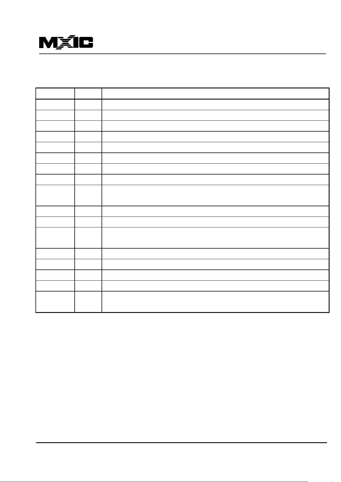
PIN DESCRIPTION
SYMBOL PIN
TYPE
PIN NBR.
PQFP
(PLCC)
DESCRIPTION
CP
I (D) 1 (18) the output of internal PLL charge pump circuits; see the end of page 21 about lock-
in
time spec.
PVDD
P (D) 2 (19) digital power supply; 5V power supply for internal PLL charge pump circuits
VCOMP
I (A) 3 (20) the reference voltage for
POW
and
BAT
comparators use
POWB
O (A) 4 (21) the output of
POW
comparator; active low
VPOW
I (A) 5 (22) the Non-inverting input of
POW
comparator; the voltage is divided from system DC
power for comparison with
VCOMP
; with 7V Surge Protect
BATB
O (A) 6 (23) the output of
BAT
comparator; active low
VBAT
I (A) 7 (24) the Non-inverting input of
BAT
comparator; the voltage is divided from battery
power for compare with
VCOMP
; with 7V surge protect
LOUTP
O (A) 8 (25) the Non-inverting output of
LIN-DRV
with PGA; PGA from 0 to 22.5dB; 1.5dB/step
LOUTN
O (A) 9 (26) the Inverting output of
LIN-DRV
with PGA; PGA from 0 to 22.5dB; 1.5dB/step
AVDD
P (A) 10 (27) analog power supply; 5V power supply for all internal analog circuits
AGND
P (A) 11 (28) analog power ground
VBG
O (A) 12 (29) band-gap reference; nominal 1.25VW and should not be used to sink or source
current
AG
O (A) 13 (30) internal analog signal ground; nominal 2.25VW and should not be used to sink or
source current
VREF
O (A) 14 (31) voltage reference; nominal 2.25VW and can sink 450uA
MIC
I (A) 15 (32) microphone input with
PRE-PGA
; PGA from -15 to 21dB;see
NOTE 1
LIN
I (A) 16 (33) telephone line signal input with
PRE-PGA
; PGA from -15 to 21dB; see
NOTE 1
AUX1
I/O (A) 17 (34) auxiliary signal input with
PRE-PGA
; PGA from -15 to 21dB; see
NOTE 1
PGAC1
O (A) 18 (35) programmable gain amplifier (
PRE-PGA
) compensative capacitor
ALCRC
O (A) 19 (36) automatic level control (
ALC
) time constant; see
FIG. 5
ALCC1
O (A) 20 (37) automatic level control (
ALC
) DC blocking capacitor output
ALCC2
O (A) 21 (38) automatic level control (
ALC
) DC blocking capacitor input
FILT
I/O (A) 22 (39) 1. anti-aliasing filter; 2. as an I/O port for
AIN
(A/D input)
PGAC2
O ( A ) 23 (40) Programmable Gain Amplifier Offset Capacitor
Page 5
MX9 3002
5
SYMBOL PIN
TYPE
PIN NBR.
PQFP
(PLCC)
DESCRIPTION
LPFC1
O (A) 24 (41) the option of the external passive
L.P.F.
(Low Pass Filter); if the pin is NC then will
by-pass L.P.F, where L.P.F. 3dB point : fc = 1/2£k∗ 3KΩ (±10%)∗ C
LPFC1
)
LPFC2
O (A) 25 (42) the option of the external passive
L.P.F.
(Low Pass Filter); if the pin is NC then will
by-pass L.P.F, where L.P.F. 3dB point : fc = 1/2£k∗ 3KΩ (±10%)∗ C
LPFC2
)
AUX2
I/O (A) 26 (43) as an I/O port for
SWK
and
SWH
VR
O (A) 27 (44) external speaker volume control; use a 10KΩ variable resistor
SVDD1
P (A) 28 (1) analog power supply; 5V power for
SPK-DRV
SPKP
O (A) 29 (2) the Non-inverting output of
SPK-DRV
with
DA-PGA, ATT1
and
ATT2
; PGA from 0
to 9dB; Attenuator 1 & 2 from 0 to -45dB; see
NOTE. 3
SGND
P (A) 30 (3) analog power ground for
SPK-DRV
SPKN
O (A) 31 (4) the Inverting output of
SPK-DRV
with
DA-PGA, ATT1
and
ATT2
; PGA from 0 to
9dB; Attenuator 1 & 2 from 0 to -45dB; see
NOTE 3
SVDD2
P (A) 32 (5) analog power ground for
SPK-DRV
SDENB
I (D) 33 (6) the enable signal for serial control data; active low; for starting to Receive/Transmit
serial control data (A2~A0,D7~D0)
SDATA
I/O (D) 34 (7) Bi-directional serial control data port; it is an interface for Microprocessor to
Transmit/Receive serial control data
SCLK
I (D) 35 (8) serial control data clock; the clock source of serial control data; from
microprocessor
DX1
O (D) 36 (9) transmit serial data
DR1
I (D) 37 (10) receive serial data
DX2
O (D) 38 (11) transmit serial data
DR2
I (D) 39 (12) receive serial data
FS
I (D) 40 (13) frame sync. input; 8KHz frame sync. Clock for the Transmit/Receive serial data
MCLK
I (D) 41 (14) master clock input, if MCLK is continuously high or low then the MX93002 will get
into power down mode automatically
VDD
P (D) 42 (15) digital power supply; 5V power supply for all internal digital logic
DGND
P (D) 43 (16) digital power ground
PGND
P (D) 44 (17) digital power ground; for internal PLL charge pump circuits
@ PIN TYPE : “I” : Input Port; “O” : Output Port; “I/O” : Bi-direction Port; “P” : Power
“(D)” : Digital Pin; “(A)” : Analog Pin
Page 6
MX9 3002
6
BASIC COMPONENTS REQUIRED
REFERANCE PART DESCRIPTION
*R1
68KΩ the resistor for internal PLL charge pump circuits
R2
2KΩ current limit resistor; to limit MIC bias current, please follow MIC specification
R3
560KΩ
ALC
release time constant; see
FIG. 10
R4, R5
to scale down DC power supply (
VPOW
) for reference to
VCOMP
to check power low
R6, R7
to scale down battery power (
VBAT
) for reference to
VCOMP
to check battery low
*C1
100pF the capacitor for internal PLL charge pump circuits
*C2
6pF the capacitor for internal PLL charge pump circuits
C8, C17
0.1uF DC blocking capacitor (0.1~10uF)
C11
0.22uF DC blocking capacitor (0.1~10uF); H.P.F.
3dB point : fc ¡Ü 1/2£k∗ 4.4KΩ ∗ C6 (0.22uF) = 164Hz
C6
10uF DC offset canceling compensative capacitor (4.7~10uF, the larger the better)
C9
0.1uF DC offset canceling compensative capacitor (0.1~1uF, the larger the better)
C3, C4, C5,
C12, C16
0.1uF De-couple capacitor (0.1~10uF)
C15
0.1uF De-couple capacitor (0.01~10uF); see
FUNCTIONAL DESCRIPTION
C10
10uF
ALC
attack time constant; see
FIG. 9
*C7
5000pF anti-aliasing capacitor
C13, C14
passive
L.P.F.
; 3dB point : fc ¡Ü 1/2£k∗ 3KΩ ∗ C13 (where C13 = C14)
*VR1
10KΩ to attenuate the input signal from
SWH
or
SWF
, if use digital volume control, then do
not need a resistor between VR and
SPKP
@ where : " * " mark shows the requirement of the component can not be changed.
Page 7
MX9 3002
7
FUNCTIONAL DESCRIPTION
. Clock Rate (REG4 bit(2))
. The clock rate (
MCLK
) must be set before user uses the function of the MX93002;
. Programmable clock rate :
1. 2.048MHz (Frame Sync. 8KHz);
2. 1.536MHz (Frame Sync. 8KHz);
. Data Format (REG4 bit(1,0))
. The data format must be set before user uses the function of the MX93002;
. Programmable Data Format
1. 16-bit linear data format. It can have 14-bit resolution and higher linearity than u/a-law format has;
2. 8-bit u-law data format;
3. 8-bit a-law data format;
. PCM CODEC
. The block includes
A/D
&
D/A
converters and all digital filters;
1.
A/D
&
D/A
Converters
A/D
Channel :
A. Input Range : 0 ~ 3Vpp (3Vpp as A/D 0dB full swing (0dBFS));
B. Digital Filters : For the purpose of out-of-band noise filtering, IIR digital filters are implemented on the
same chip ( >26dB / 60Hz; <1dB / 300Hz ~ 3.4KHz; >14dB / 3.6KHz ~ 4.6KHz; >32dB / >4.6KHz );
D/A
Channel :
A. Output swing : 0 ~ 3Vpp (3Vpp as D/A 0dB full swing (0dBFS));
B. Digital Filters :
a. G.711 specification;
b. The digital input applied to D/A converter can not be a DC signal other than idle (bits all zero), as
limit cycles in the embodiment method at a level of -70dBm will present at the analog output.
. Power Down Mode
. The MX93002 will recover from power-down mode when MCLK keeps a consistent clock (1.536 or 2.048MHz);
. Support system power (Adapter and Battery) detection. The function will work well even under 3V power supply;
. Support automatic power-down control when
MCLK
keeps high or low;
. Support 4 power-down modes for special applications:
MODE
FUNCTION
REG 6 (7,6)
(SLEEPA,SLEEP) = ( 0,0 )
REG 6 (7,6)
(SLEEPA,SLEEP) = ( 0,1 )
REG 6 (7,6)
(SLEEPA,SLEEP) = ( 1,0 )
REG 6 (7,6)
(SLEEPA,SLEEP) = ( 1,1 )
VBG
reference on off off on
POW
&
BAT
on off on on
all analog blocks off off off on
A/D and D/A off off off off
Table 1
Page 8
MX9 3002
8
. 3-Channel Input (MIC,AUX1,LIN) with PRE-PGA (Pre-Programmable Gain Control)
. Input Range : 0 ~ AVDD-2Vpp;
.
PRE-PGA
gain step from 21dB to -15dB (21, 18, 15, 12, 9, 7.5, 6, 4.5, 3, 0, -3, -6, -9, -12, -15dB);
. Driving Capacity : more than 400uA at
FILT
and
AUX2
output;
. Input Impedance : more than 25KΩ;
. THD : less than 70dB at
FILT
output;
. There is just one path which can be selected at the same time;
. The gain setting of the path will be mapped to the
PRE-PGA
when user changes the path of Input.
. ALC (Automatic Level Control)
. Input Range : 0 ~ 1.2Vpp (Loop Gain : 40dB);
. Output Characteristic : see
FIG. 5
~
FIG. 7
;
. Loop Gain : 42dB max (with external RC time constant);
. Driving Capacity : more than 400uA at
FILT
and
AUX2
output;
. THD : less than 40dB at
FILT
output (Loop Gain : 40dB).
. AD1 PGA
. Input Range : 0 ~ AVDD-2Vpp;
.
AD1-PGA
can support gain step from 0dB to 18dB (0, 4, 8, 18dB);
. AD2 PGA
. Input Range : 0 ~ AVDD-2Vpp;
.
AD2-PGA
can support gain step from -6dB to 39dB (-6, -3, 0, 3, 6, 9, 12, 15, 18, 21, 24, 27, 30, 33, 36, 39dB);
. FILT as I/O Port
. Input Range : 0 ~ AVDD-2Vpp;
. Input Impedance : more than 1KΩ;
. Output Impedance : less than 1KΩ;
. Load Capacitance : 5000pF;
. AUX1 & AUX2 as I/O Port
. Input Range : 0 ~ AVDD-2Vpp;
. Input Impedance : more than 15KΩ;
. Output Impedance : less than 15KΩ;
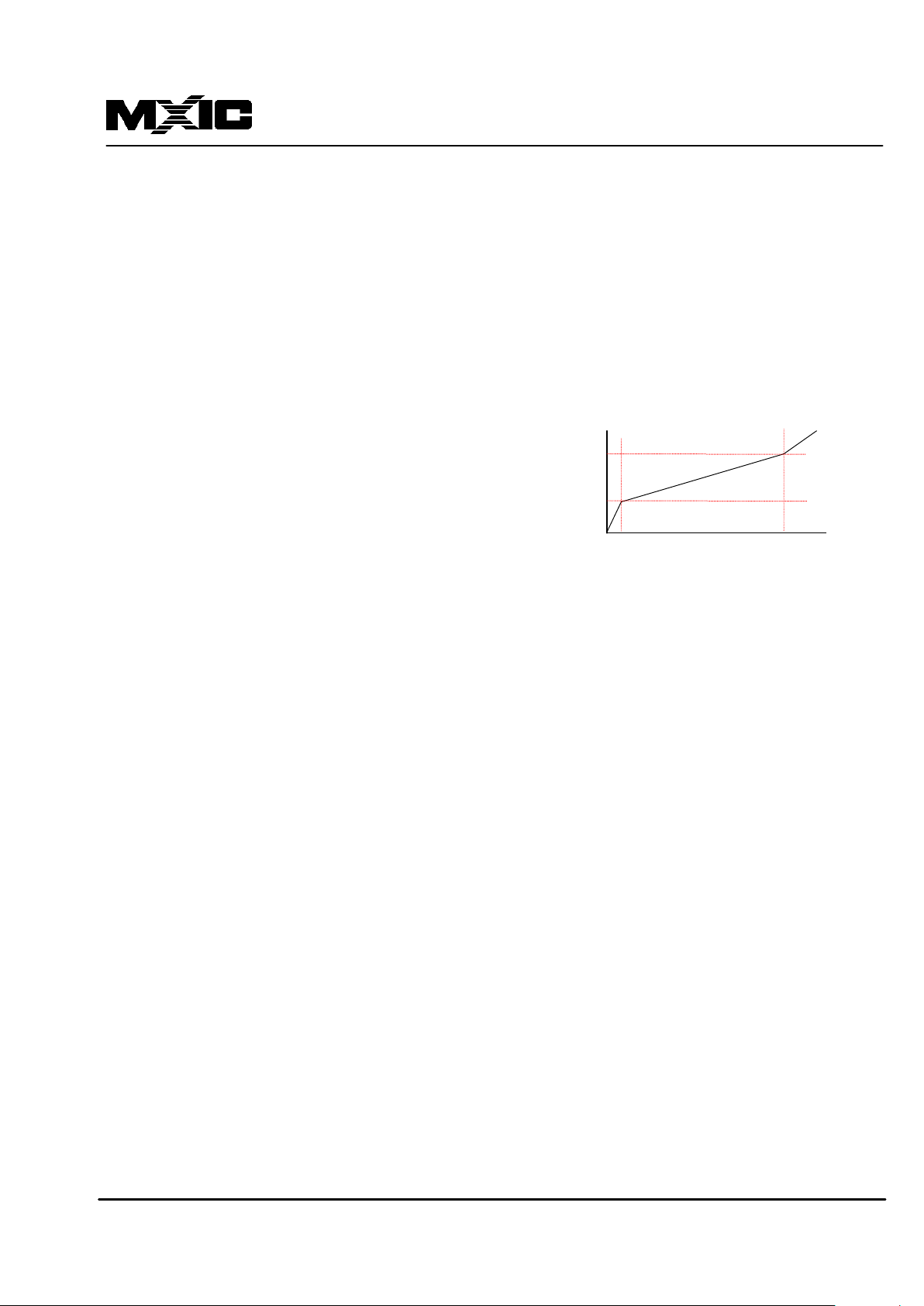
. External passive L.P.F. (Low Pass Filter)
. External capacitors (
LPFC1
and
LPFC2
) can be changed to attenuate high frequency noise at
SPKP
and
SPKN
output;
. When external capacitors (
LPFC1
and
LPFC2
) are NC (no connection), then passive
L.P.F.
will be by-passed;
. Output of the Line Driver (
LOUTP
and
LOUTN
) can be chosen to pass or by-pass the
L.P.F.
;
.
LPFC1/LPFC2
can be a D/A output pin and output impedance is around 3KΩ/6KΩ;
3000mVpp
VOUT ( mVpp )
1000mVpp
10mVpp 1200mVpp
VIN ( mVpp )
Page 9

MX9 3002
9
. Line Driver (
LIN-DRV
)
. Not only support the programmable gain from 0 to 22.5dB, but also fully differentially drive 6Vpp over 600Ω;
. If switches
SWE, SWJ, SWK
and
SWL
are opened, then the line driver will be muted to -70dB and power-down
automatically;
1. output swing : Single Ended (only use
LOUTP
or
LOUTN
) : 0 ~ 3Vpp (over 600Ω load, at LIN-DRV = 0dB);
Fully differential (use
LOUTP + LOUTN
) : 0 ~ 6Vpp (over 600Ω load, at LIN-DRV = 0dB);
2.
LIN-DRV
gain step from 0dB to 22.5dB (1.5dB/step);
3. THD : less than 70dB at 6Vpp output over 600Ω load;
. D/A PGA
. Input Range : 0 ~ AVDD-2Vpp;
.
DA-PGA
can support gain step from 0dB to 6dB (2dB/step);
. Attenuator (
ATT1
&
ATT2
)
. Speaker output signal can be attenuated either by internal register or external resistor;
. If switches
SWF
and
SWH
are opened, then attenuator will be muted to -70dB automatically;
1.
ATT1
(internal register) : 16 steps programmable, from -45dB to 0dB (-45, -39, -33, -27, -24, -21, -18, -15,
-12, -9, -7.5, -6, -4.5, -3, -1.5, 0dB);
2.
ATT2
(external variable resistor) : from -45 ~ 0dB (determined by external 10KΩ potentiometer);
3. THD : less than 70dB;
4. input range for
AUX2
: 0 ~ AVDD-2Vpp;
5. input impedance for
AUX2
: more than 15KΩ;
. Speaker Driver (SPK-DRV)
. If switches
SWF
and
SWH
are opened, then
SPK-DRV
will be power-down automatically;
1. Maximum output swing : 6Vpp with 8Ω load at fully differential output (
SPKP + SPKN
);
2. THD : less than 60dB (at 6Vpp/8Ω load);
. Voltage Reference (VREF & VAG)
. Two 2.25VW voltage references are on-chip generated, where
VREF
is for external circuit use and
VAG
is for
internal circuit use;
.
VREF
can be used to bias the microphone, the level shift circuit or other applications;
1.
VREF
driving capacity : more than 400uA;
2. User can use the
VREF
to provide DC bias to external components;
. Bandgap Reference (VBG)
. A bandgap circuit generates a voltage source (
VBG
) which is around 1.2VW. It is with low temperature
coefficient and good power supply rejection;
. If user changes VBG bypass capacitor (C15) then the MX93002 warm-up time will be changed; see
The Timing
Diagram of CODEC Function;
Page 10

MX9 3002
10
. Serial Control Interface
. Use
SCLK
for synchronization with
SDATA
to read/write the internal control registers;
. All registers will keep original setting when the MX93002 returns from power-down or sleep mode;
1. When
SDENB
(serial data enable) signal active low, the MX93002 starts to receive serial control data
(
SDATA
);
2. Set
SDENB
from low to high when transmitting
SDATA
is complete;
3.
SDATA
format : 3 addresses from A2 to A0, 8 data from D7 to D0 (A2 is MSB and D0 is LSB);
. Two Comparators for System Applications (RING and CPC)
. To detect Ring and CPC (Calling Party Control) or other applications;
1. input range : 0 ~ AVDD-2Vpp (with 7V surge protection);
2. input impedance : more than 10^12Ω ;
3. input offset voltage : less than 10mV;
4. output impedance : less than 10KΩ;
5. slew rate : 3V/us max.;
. Switches
. There are three registers (REG0, REG3 and REG6) which are used to control all of the switches so that user
can direct many different signal paths, for examples:
1. Record signal from
MIC
and play signal to
SPKP/N
or play signal to
LOUTP/N
:
A. Record signal from
MIC
or Record signal from
LIN
:
a. System initialization [set
MIC
gain (REG2 bit(3~0)), set
LIN
gain (REG1 bit(7~4), set
ALC
gain
0/6dB (REG5 bit(1)) and set
A/D-PGA
gain (REG6 bit(1,0))]
b. Record signal from
MIC
: set REG0 = 0X0048
MIC
⇒
SWA
⇒
PRE-PGA ⇒ SWC (ALC
on) ⇒
SWD
⇒
AD1-PGA
⇒
PCM CODEC AIN1
c. Record signal from
LIN
: set REG0 = 0X00C8
LIN
⇒
SWA
⇒
PRE-PGA
⇒
SWC (ALC
on) ⇒
SWD
⇒
AD1-PGA
⇒
PCM CODEC AIN1
B. Play signal to
SPKP/N
or play signal to
LOUTP/N
:
a. System initialization [fix the value of
L.P.F.
, set (REG6 bit(5)), set
D/A-PGA
gain (REG6 bit(3,2), set
ATT1
gain (REG3 bit(3~0)) and
LIN-DRV
gain (REG1 bit(3~0))]
b. Play signal to
SPKP/N
(use digital volume control) : set REG 0 = 0X0003
PCM CODEC AOUT1
⇒
L.P.F.
⇒
SWF
⇒
DA-PGA ⇒ SWG (ATT1
) ⇒
SPK-DRV
⇒
SPKP/N
c. Play signal to
LOUTP/N
: set REG 0 = 0X0004
i.
PCM CODEC AOUT1
⇒
L.P.F.
⇒
SWL ⇒ LIN-DRV
⇒
LOUTP/N
ii.
PCM CODEC AOUT2
⇒
SWE
⇒
LIN-DRV
⇒
LOUTP/N
d. Play signal to
SPKP/N
(use digital volume control) and
LOUTP/N
: set REG 0 = 0X0007
i.
PCM CODEC AOUT1
⇒
L.P.F. ⇒ SWF
⇒
DA-PGA
⇒
SWG (ATT1
) ⇒
SPK-DRV
⇒
SPKP/N
PCM CODEC AOUT2
⇒
SWE
⇒
LIN-DRV
⇒
LOUTP/N
ii.
PCM CODEC AOUT1
⇒
L.P.F. ⇒ SWF
⇒
DA-PGA
⇒
SWG (ATT1
) ⇒
SPK-DRV
⇒
SPKP/N
⇒
SWL
⇒
LIN-DRV
⇒
LOUTP/N
Page 11
MX9 3002
11
2. Room Monitoring:
A. System initialization [set
MIC
gain (REG2 bit(3~0)), set
ALC
gain 0/+6dB (REG5 bit(1)), set
LIN-DRV
gain (REG1 bit(3~0)), set REG3 bit(6,5) and set REG6 bit(1,0)]
B. Switches path:
a. Remote Monitoring:
MIC
⇒
SWA
⇒
PRE-PGA
⇒
SWC (ALC
on) ⇒
SWJ
⇒
LIN-DRV
⇒
LOUTP/N
b. Local Detecting DTMF:
LIN
⇒
SWI
⇒
AD1-PGA
⇒
PCM CODEC AIN1
3. Digital Speakerphone:
A. System Initialization [set
MIC
gain (REG2 bit(3~0)), set
AD1-PGA
gain (REG6 bit(1,0)), fix the value of
L.P.F.
, set
DA-PGA
gain (REG6 bit(3,2)), set
ATT1
gain (REG3 bit(3~0)), set
LIN
gain (REG1 bit(7~4)), set
SWM
REG4 bit(4), set
LIN-DRV
gain (REG1 bit(3~0))]
B. Switches path : set REG0 = 0X00AF
a. CODEC 1 : Record signal from
MIC
and Play signal to
SPKP/N
(use digital volume control)
MIC
⇒
SWA
⇒
PRE-PGA
⇒
SWC (ALC
off) ⇒
SWD
⇒
AD1-PGA
⇒
PCM CODEC AIN1
PCM CODEC AOUT1
⇒
L.P.F.
⇒
SWF ⇒ SWG (ATT1
) ⇒
SPK-DRV
⇒
SPKP/N
b. CODEC 2 : Record signal from
LIN
and Play signal to
LOUTP/N
LIN
⇒
SWM
⇒
AD2-PGA
⇒
PCM CODEC AIN2
PCM CODEC AOUT2
⇒
SWE
⇒
LIN-DRV
⇒
LOUTP/N
. Power Consumption (with 600Ω line load and 8Ω speaker load)
Max. Power
Consumption
Operation
LIN-DRV
Dis/Enable
SPK-DRV
Dis/Enable
Analog
circuits
Digital
circuits
Unit
Stand-by Disable Disable 27 8 mA
Operating
Disable
Enable
Disable
Enable
Disable
Disable
Enable
Enable
27
31
240
250
8
8
8
8
mA
Power-down Disable Disable 460 335 uA
Power-down with SLEEP = 1 Disable Disable 20 400 uA
@ Test condition : 1. at
LIN-DRV
(with 600Ω load) /
SPK-DRV
(with 8Ω load) full swing output
2. see
LIN-DRV
and
SPK-DRV
Descriptions
3. at the case of Temperature from -2¢J to 72¢J and Voltage from 4.4V to 5.6V
Page 12

MX9 3002
12
CONTROL REGISTERS DEFINITION
REGISTER 0
ADDRESS BIT A2 A1 A0
DATA
0 0 0
DATA BIT D7 D6 D5 D4 D3 D2 D1 D0
POWER-ON
0 0 0 0 0 0 0 0
DESCRIPTION SWA SWB SWC SWD SWE SWF SWG
(
SWA
) D(7,6) = (1,1) : path of
SWA
is "c ⇒ A",
PRE-PGA
setting follows
LIN
GAIN SETTING
= (1,0) : path of
SWA
is "b ⇒ A",
PRE-PGA
setting follows
AUX1
GAIN SETTING
= (0,1) : path of
SWA
is "a ⇒ A",
PRE-PGA
setting follows
MIC
GAIN SETTING
= (0,0) : path of
SWA
is "d ⇒ A", (GROUNDING to AG)
(
SWB
) D(5) = (1) : path of
SWB
is "CLOSE", D(5) = (0) : path of
SWB
is "OPEN"
(
SWC
) D(4) = (1) : path of
SWC
is "b ⇒ A", D(4) = (0) : path of
SWC
is "a ⇒ A"
(
SWD
) D(3) = (1) : path of
SWD
is "CLOSE", D(3) = (0) : path of
SWD
is "OPEN"
(
SWE
) D(2) = (1) : path of
SWE
is "CLOSE", D(2) = (0) : path of
SWE
is "OPEN"; see
NOTE 4
(
SWF
) D(1) = (1) : path of
SWF
is "CLOSE " , D(1) = (0) : path of
SWF
is " OPEN "
(
SWG
) D(0) = (1) : path of
SWG
is "a ⇒ A",
ATTENUATOR 1 (ATT1)
= (0) : path of
SWG
is "a ⇒ B",
ATTENUATOR 2 (ATT2)
REGISTER 1
ADDRESS BIT A2 A1 A0
DATA
0 0 1
DATA BIT D7 D6 D5 D4 D3 D2 D1 D0
POWER-ON
0 0 0 0 0 0 0 0
DESCRIPTION LIN
GAIN SETTING (
PRE-PGA
)
LIN-DRV
GAIN SETTING
(
LIN
GAIN SETTING ) D(7~4) = (F) ~ (0) : 21dB ~ -15dB; see
NOTE 1
(
LIN-DRV
GAIN SETTING ) D(3~0) = (F) ~ (0) : 22.5dB ~ 0dB 1.5dB/step; see
NOTE 2
REGISTER 2
ADDRESS BIT A2 A1 A0
DATA
0 1 0
DATA BIT D7 D6 D5 D4 D3 D2 D1 D0
POWER-ON
0 0 0 0 0 0 0 0
DESCRIPTION AUX1
GAIN SETTING (
PRE-PGA
)
MIC
GAIN SETTING (
PRE-PGA
)
(
AUX1
GAIN SETTING ) D(7~4) = (F) ~ (0) : 21dB ~ -15dB; see
NOTE 1
(
MIC
GAIN SETTING ) D(3~0) = (F) ~ (0) : 21dB ~ -15dB; see
NOTE 1
Page 13

MX9 3002
13
REGISTER 3
ADDRESS BIT A2 A1 A0
DATA
0 1 1
DATA BIT D7 D6 D5 D4 D3 D2 D1 D0
POWER-ON
0 0 0 0 1 1 1 1
DESCRIPTION SWH SWI SWJ SWK ATT1
GAIN SETTING
(
SWH
) D(7) = (1) : path of
SWH
is "CLOSE", D(7) = (0) : path of
SWH
is "OPEN”
(
SWI
) D(6) = (1) : path of
SWI
is "CLOSE", D(6) = (0) : path of
SWI
is "OPEN"
(
SWJ
) D(5) = (1) : path of
SWJ
is "CLOSE", D(5) = (0) : path of
SWJ
is "OPEN"
(
SWK
) D(4) = (1) : path of
SWK
is "CLOSE", D(4) = (0) : path of
SWK
is "OPEN"
(
ATT1
GAIN SETTING ) D(3~0) = (F)~(0) : - 45dB ~ 0dB; see
NOTE 3
REGISTER 4
ADDRESS BIT A2 A1 A0
DATA
1 0 0
DATA BIT D7 D6 D5 D4 D3 D2 D1 D0
POWER_ON
0 1 0 1 1 0 0 0
DESCRIPTION AD2-PGA
GAIN SETTING
SWM
RATE DATA FORMAT
(
AD2-PGA
GAIN SETTING ) D(7~4) = (0) ~ (F) : -6dB ~ 39dB; see
NOTE 3
(
SWM
) D(3) = (1) : path of
SWM
is "CLOSE", D(3) = (0) : path of
SWM
is "OPEN"
( RATE ) D(2) = (1) : master clock (
MCLK
) use 1.536MHz, D(2) = (0) : master clock (
MCLK
) use 2.048MHz
( DATA FORMAT ) D(1,0) = (1,1),(1,0) : Linear Coder/Decoder (16-bit format)
= (0,1) : a-Law Coder/Decoder (8-bit format)
= (0,0) : u-LAW Coder/Decoder (8-bit format)
@ Linear 16-bit format : 14-bit resolution with 2 LSB = 0
SIGN \ SCALE MIN MAX
POSITIVE
0000 0000 0000 0000 0111 1111 1111 1100
NEGATIVE
1111 1111 1111 1100 1000 0000 0000 0000
REGISTER 5
ADDRESS BIT A2 A1 A0
DATA
1 0 1
DATA BIT D7 D6 D5 D4 D3 D2 D1 D0
POWER_ON
0 0 0 0 0 0 0 0
DESCRIPTION
ALC1 SPKHI ADA AIADID DAYT ADYT ALC0 TDSPCK
D ( 5 ~ 2 and 0 ) : reserved
( SPKHI ) D(6) = (0) :
SPKP/N
can drive 8Ω load when
SPK-DRV
turns on
D(6) = (1) :
SPKP/N
appears high impedance (10KΩ) and
SPK-DRV
will keep a quiescent current when
Page 14

MX9 3002
14
SPK-DRV
turns on
( ALC1 , ALC0 ) D(7,1) = (0,0) :
ALC
open loop gain is 38dB
= (0,1) :
ALC
open loop gain is 42dB
= (1,0) : reserved
= (1,1) : external
ALC
option (
PRE-PGA
Output :
ALCC1, SWC
path “a” Input :
ALCC2
)
REGISTER 6
ADDRESS BIT A2 A1 A0
DATA
1 1 0
DATA BIT D7 D6 D5 D4 D3 D2 D1 D0
POWER_ON
0 0 0 0 0 0 0 0
DESCRIPTION
SLEEPA SLEEP
SWL
SPK-
MUTE
SPK-DRV
GAIN
SETTING
AD1-PGA
GAIN
SETTING
( SLEEPA , SLEEP ) D(7,6) = (0,0) : when the MX93002 gets into power down mode, all the blocks of the MX93002
will be disabled except the
VBG
reference and 2 comparators (
POW, BAT
)
D(7,6) = (0,1) : when the MX93002 gets into power down mode, all the blocks of the MX93002
will be disabled
D(7,6) = (1,0) : when the MX93002 gets into power down mode, all the blocks of the MX93002
will be disabled except 2 comparators (
POW, BAT
)
D(7,6) = (1,1) : when the MX93002 gets into power down mode, all the analog blocks of the
MX93002 will be still functional and can be programmed by control registers
(
SWL
) D(5) = (1) : path of
SWL
is "CLOSE", D(5) = (0) : path of
SWL
is "OPEN”; see
NOTE 7
( SPK-MUTE ) D(4) = 1 : force
SPK-DRV
mute to -70dB, D(4) = 0 : force
SPK-DRV
un-mute
(
SPK-DRV
GAIN SETTING ) D(3,2) = (0,0) ~ (1,1) : 0dB ~ 8dB; 2dB/step; see
NOTE 5
(
AD1-PGA
GAIN SETTING ) D(1,0) = (0,0) ~ (1,1) : 0dB ~ 18dB; see
NOTE 2
REGISTER 7
ADDRESS BIT A2 A1 A0
DATA
1 1 1
DATA BIT D7 D6 D5 D4 D3 D2 D1 D0
POWER_ON
0 0 0 0 0 0 0 0
DESCRIPTIN SWO SWN
READ REGISTER ADDRESS
(
SWO
) D(5) = (1) : path of
SWO
is "CLOSE", D(5) = (0) : path of
SWO
is "OPEN”
(
SWN
) D(4) = (1) : path of
SWN
is "CLOSE", D(5) = (0) : path of
SWN
is "OPEN”; see
NOTE 7
( READ ) D(3) = 1 : read data from Register 0 ~ 7, D(3) = 0 : write data to Register 0 ~ 7
( REGISTER ADDRESS ) D(2~0) : When READ = 1, then
a. READ will be cleared automatically;
b. if next uP
SDENB
signal active low, the content of REGISTER ADDRESS will be dumped out through
CODEC
SDATA
interface;
Page 15

MX9 3002
15
SPECIFICATIONS
Absolute Maximum Rating
PARAMETER MIN TYP MAX UNITS
AVDD to AGND
VDD to DGND
Voltage at any Digital Input or Output
Current at any Digital Input or Output
Operating Ambient Temperature Range
Storage Temperature Range
Lead Temperature ( Soldering, 10 seconds )
-0.3
-0.3
DGND-0.3
0
-65
6.0
6.0
VDD+0.3
8
70
150
V
V
V
mA
¢J
¢J
Power Supply
PARAMETER MIN TYP MAX UNITS
Power Supply Voltage :
Digital and Analog
Power Supply Current :
Stand-by :
Digital
Analog
Operating :
Digital
Analog ( see Page 11)
Power-Down :
Digital
Analog ( at REG4 bit 6 SLEEP = 0 )
Analog ( at REG4 bit 6 SLEEP = 1 )
4.5 5.0 5.5
8
27
8
255
400
460
20
V
mA
mA
mA
mA
uA
uA
uA
Electrical Characteristics
(
BOLD
characters are guaranteed for AVDD = VDD = 5V ±5%, temperature =
0 ~ 70¢J. Typical specified at AVDD = VDD = 5V, temperature = 25¢J. “*” mark : guaranteed by
design )
Digital Interface
PARAMETER MIN TYP MAX UNITS
High Level Input Voltage ( VIH )
Low Level Input Voltage ( VIL )
High Level Output Voltage ( VOH )
Low Level Output Voltage ( VOL )
Input Low Current ( IIL )
2.2
2.4
-10
±2
0.6
0.4
10
V
V
V
V
uA
Page 16

MX9 3002
16
Input High Current ( IIH )
-10 10
uA
Analog Input Ports
PARAMETER MIN TYP MAX UNITS
MIC / LIN / AUX1 :
Input Voltage
* Input Capacitance
* Input Impedance 20
3.0
15
Vpp
pF
KΩ
Analog Output Ports
PARAMETER MIN TYP MAX UNITS
Line Driver :
Gain Range
Step Size
Step Variation
Fully Differential (LOUTP+LOUTN) Full Swing / with 600Ω load
Single Ended (LOUTP) Full Swing / with 600Ω load
* External Load Capacitance
* Output Impedance
0
±1.5
±10
6.0
3.0
600
22.5
200
dB
dB
%
Vpp
Vpp
pF
Ω
Speaker Driver :
Fully Differential (SPKP+SPKN) Full Swing / with 8Ω load
Single Ended (SPKP) Full Swing / with 8Ω load
* External Load Capacitance
* Output Impedance
the Quiescent current (when REG5 bit(6) SPKHI = 1)
6.0
3.0
100
8
4
Vpp
Vpp
pF
Ω
mA
Analog I/O Ports
PARAMETER MIN TYP MAX UNITS
FILT :
as Input Port :
* Input Capacitance
* Input Impedance
as Output Port :
* External Load Capacitance
* Output Impedance
5000
1
5000
1
pF
KΩ
pF
KΩ
AUX2 :
as Input Port :
* Input Capacitance
* Input Impedance
as Output Port :
* External Load Capacitance
15
15
15
pF
KΩ
pF
Page 17

MX9 3002
17
* Output Impedance 15 KΩ
Gain Variation
PARAMETER MIN TYP MAX UNITS
PRE-PGA :
Gain Range
Step Size
Step Variation
-15
±1.5, ±3
±10
22.5 dB
dB
%
AD1-PGA :
Gain Range
Step Size
Step Variation
0
±4, ±10
±10
18 dB
dB
%
AD2-PGA :
Gain Range
Step Size
Step Variation
-6
±3
±10
39 dB
dB
%
DA-PGA :
Gain Range
Step Size
Step Variation
0
±2
±10
6 dB
dB
%
Attenuator
PARAMETER MIN TYP MAX UNITS
Attenuator 1 ( Digital Volume ) :
Gain Range
Step Size
Step Variation
* Mute Attenuation
-45
-57
±6, ±3, ±1.5
±10
0 dB
dB
%
dB
Attenuator 2 ( External Volume ) :
Gain Range
the Requirement of External Resistor ( from SPKP to VR )
* Mute Attenuation
-45
-57
10
0 dB
KΩ
dB
Bandgap ( VBG pin )
PARAMETER MIN TYP MAX UNITS
Output Voltage
* Output Current
1.16 1.2
Hi-z
1.24 V
Voltage Reference ( VREF pin )
PARAMETER MIN TYP MAX UNITS
Page 18

MX9 3002
18
Output Voltage
* Output Current
2.0 2.25
450
2.5 V
uA
Two Operational Amplifier / Comparators ( RING, CPC )
PARAMETER MIN TYP MAX UNITS
* Input Offset Voltage
* Input Voltage
* Input Impedance
* Output Impedance
* Open Loop Gain
* Unit Band Gain Width
* Slew Rate
* Input Comm. Mode Range
10^12
10
3.5
10
7
78
2
3
mV
V
Ω
KΩ
dB
MHz
V / us
V
Two Comparators ( POW, BAT )
PARAMETER MIN TYP MAX UNITS
Input Voltage (VCOMP, VPOW, VBAT)
* Hysteresis
* Output Impedance of POWB and BATB pins 10
15
AVDD V
mV
KΩ
Page 19

MX9 3002
19
TIMING DESCRIPTION
TIMING DESCRIPTION MIN TYP MAX UNIT
1/Tmck
frequency of master clock (from Vmckh1 to next Vmckh1) at RATE = 0
1.638 2.048 2.560
MHz
Trmck
rise time of master clock
50
ns
Tfmck
fall time of master clock
50
ns
Tfs
from Vmckh1 to Vfsh1
0
ns
Tfsh
holding time for frame sync. From Vfsh1 to Vfsh2
MCLK
ns
Tdxs
setting time for CODEC transmit data from Vmckh1(n) to DX(n) data ready
110
ns
Tdrh1
holding time for CODEC received data from DR(n) data ready to Vmckh2(n)
0
ns
Tdrh2
holding time for CODEC received data from Vmckl(n) to DR(n) ending
150
ns
Tupen1
from Vsclkh1 to Venl
40 SCLK
ns
Tupen2
from Vsclkh1 to Venh
40 SCLK
ns
Tups1
setting time for uP transmitting SDATA from Vupenl to uP SDATA(n) ready
( @ where Tupen1+Tups1 must < SCLK )
40 SLCK
ns
Tups2
setting time for uP transmitting SDATA from Vsclkh1(n+1) to uP
SDATA(n+1) ready
40 SCLK
ns
Tuph
holding time for uP transmitting SDATA from Vsclkh1(n+1) to uP SDATA(n)
ending
40 Tups2
ns
Tcdrd
from Vsclkh1(n+1) to CODEC reading SDATA(n)
20
ns
Tupo2i
from Vupenl to uP changing its SDATA interface to input port
40 FS
ns
Tcdi2o
from Vsclkh1 to CODEC changing its SDATA interface to output port
20
ns
Tcds1
setting time for CODEC transmitting SDATA from Vcdi2o to SDATA(n)
ready
20
ns
Tcds2
setting time for CODEC transmitting SDATA from Vsclkh1(n+2) to
SDATA(n+1) ready
20
ns
Tcdh
holding time for CODEC transmitting SDATA from SDATA(n) ready to
Vsclkh1(n+2)
SCLK
ns
Tcdo2i
from Venh to CODEC changing its SDATA interface to input port
20
ns
Tuprd
from Vsclkh1(n+1) to uP reading SDATA(n)
40 SCLK
ns
Tupi2o
from Vsclkh1 to uP changing its SDATA interface to output port
40 FS
ns
Vmckh1
logic high when CODEC MCLK rising
Vmckh2
logic high when CODEC MCLK falling
Vmckl
logic low when CODEC MCLK falling
Vfsh1
logic high when CODEC FS rising
Vsclkh1
logic high when SCLK rising
Vcdi2o
CODEC changes its SDATA interface to output port
Venh
logic high when uP SDENB rising
Venl
logic low when uP SDENB falling
Page 20

MX9 3002
20
TIMING DIAGRAM
Master Clock, Frame Sync. & Data Timing Diagram
1 2 3 4
6
7 8
Tfs
Tfsh
Tdxs
Tdxs
MCLK
FS
DX
1 2
1
2
9
1
0
1
1
1
2
1
3
1
4
1
5
1
6
1 2
3 4
5 6 7 8
1
2
3 4 5
6
7
8
9
10
11
12 13 14 15
16
MCLK
FS
u/a-law
DR / DX
Linear
DR / DX
DR
1
2
Tdrh2
Tdrh1
MSB
LSB
LSBMSB
Vmckh1
Vmckh2
Vmckl
Vfsh1
Vfsh2
Vmckh1
(n)
(n+1)
(n) (n+1)
(n) (n+1)
5
L
u-law : H , a-law : L
Control Registers R/W Timing Diagram
SCLK
SDENB
1
2
3 4
5
6
7
A2 A1 A0 D7 D6
D5
D4 D3
D2 D0
8 9
1
0
1
1
1
2
1
3
Vsclkh1
uP SDATA
interface
Tupen1
Tcds1
uP read SDATA
Tuprd
CODEC SDATA
interface
Tupen2
CODEC WRITE SDATA
Tcdo2i
Tupi2o
Tcdi2o
Tupo2i
Vcdi2o
Tcdh
n+2
n+1
n+1
SCLK
SDENB
1
2
3 4
5
6
7 8 9
1
0
1
1
1
2
1
3
Vsclkh1
uP SDATA
interface
Tupen1
Tups1
CODEC read SDATA
CODEC SDATA
interface
Tupen2
CODEC READ SDATA
Tcdrd
Tups2
Venl
Venh
Tuph
Tuph
n+1
n+2
D1
A2 A1
A0 D7 D6 D5
D4 D3 D2 D0D1
Tcds2
n
n
n
n+1n
Page 21

MX9 3002
21
The Timing Diagram of CODEC Function
(SLEEPA,SLEEP) = (0,0) or (1,1)
tA tB tC tD tE tF tG tJ
VBG
MCLK
POW, BAT
2 OPs
VAG
tK
VDD
AVDD
tH
@ Analog Paths : Analog I/O, Switches, PGA and Attenuator
Analog Paths
Register
R/W
A/D and D/A
CP
tL tMt I
Analog Paths
power-down
MCLK keeps Hi or Lo
@ : Stable
(SLEEPA,SLEEP)
= (0,0)
(SLEEPA,SLEEP)
= (1,1)
~ 1.2V
(SLEEPA,SLEEP) = (0,1) or (1,0)
ta tb tc td te tf tg tj
VBG
MCLK
POW, BAT
2 OPs
VAG
tk
VDD
AVDD
th
@ Analog Paths : Analog I/O, Switches, PGA and Attenuator
Analog Paths
Register
R/W
A/D and D/A
CP
tl tmti
power-down
MCLK keeps Hi or Lo
@ : Stable
(SLEEPA,SLEEP)
= (0,1)
(SLEEPA,SLEEP)
= (1,0)
POW, BAT
2 OPs
tn
~ 1.2V
~ 3.4V
Page 22

MX9 3002
22
The Timing Description of CODEC Function
TIMING DESCRIPTION MIN TYP MAX UNIT
tA, ta
VDD
/
AVDD
¡Ü 3.0VDC
tC MCLK
started
tC ⇒ tG
tc ⇒ tg
MCLK
keeps
tG, tg
Power-down started (
MCLK
keeps High or Low )
tJ, tl
Power-down ended (
MCLK
started )
tF ⇒ t I MCLK
keeps High or Low
tA ⇒ tB
ta ⇒ tb
the charge time of
VBG
( where
VBG
bypass cap. = 0.1uF ) 140 190 290 ms
tC ⇒ tD
tJ ⇒ tK
tc ⇒ td
tk ⇒ tl
the charge time of internal clock detector circuit 20 us
tD ⇒ tE
tK ⇒ tL
td ⇒ te
tl ⇒ tm
the lock-in time of PLL ( C1=100pF, C2=6pF, R1=68KΩ ) 50 110 160 us
tD ⇒ tF
tK ⇒ tM
td ⇒ tf
the charge time of
VAG
( where
VAG
bypass cap. = 0.1uF ) 1.5 2 2.5 ms
tG ⇒ tH
tg ⇒ th
the discharge time of internal clock detector circuit 50 us
tH ⇒ tI
th ⇒ tj
the discharge time of
VAG
( where
VAG
bypass cap. = 0.1uF ) 0.3 0.5 0.7 ms
th ⇒ ti
the delay time of
VBG
disable ( where
VBG
bypass cap. = 0.1uF ) 6 10 15 ms
tl ⇒ tn
the re-charge time of
VBG
( where
VBG
bypass cap. = 0.1uF )
the re-charge time of
VAG
( where
VAG
bypass cap. = 0.1uF )
400 500 700 ms
@ when change
VBG
bypass capacitor (C15) :
i. from 0.1uF to 1uF : (
tA ⇒ tB
)’ ¡Ü 10 ∗ (
tA ⇒ tB
)
ii. from 0.1uF to 0.01uF : (
tA ⇒ tB
)’ ¡Ü 1/10 ∗ (
tA ⇒ tB
)
Page 23

MX9 3002
23
A/D Path Characteristics
( 0dBFS : reference to Fin = 1.02KHz and A/D Input is Full Swing )
PARAMETER MIN TYP MAX UNITS
Dynamic Range ( at -51dBFS )
THD+N ( at Vin = -6dBFS )
Interchannel Isolation of LIN/MIC/AUX1 ( at Vin = 0dBFS )
Gain Variation ( at Vin = -6dBFS )
Max. Overload Level
Frequency Response ( Measure Respone from 60Hz to
4000Hz, see FIG. 3 ) :
60Hz
150Hz
200Hz
300 ~ 3200Hz
3400Hz
3600Hz
3800Hz
4000Hz
4500Hz and Up
77
-56
-0.3
3.0
-25
-0.8
-1.60
-10.3
-69.5
76
3.25
-7
-3
-4.5
-45
0.3
3.50
-28
-8
-4
+0.8
-1.85
-10.7
dB
dB
dB
FS
dB
FS
Vpp
dB
dB
dB
dB
dB
dB
dB
dB
dB
D/A Path Characteristics
( 0dBFS : reference to Fout = 1.02KHz and D/A Output is Full Swing )
PARAMETER MIN TYP MAX UNITS
Dynamic Range ( at -51dBFS )
THD+N ( at Vin = -6dBFS )
Gain Variation ( at Vin = -6dBFS )
Out of Band Energy ( with 1.02KHz Image ) :
3.8KHz ~ 20KHz
Output Level ( at AUX2 )
Frequency Response ( Measure Respone from 60Hz to
3800Hz, see FIG. 4 ) :
60Hz ~ 300Hz
300Hz ~ 2800Hz
3000Hz
3200Hz
3400Hz
3600Hz
3800Hz
77
-47
-46
- 0.6
± 0.1
3.0
-0.1
-1.1
-2.1
-3.7
-6.3
-10
+ 0.1
dB
dB
dB
FS
dB
FS
Vpp
dB
dB
dB
dB
dB
dB
dB
Page 24

MX9 3002
24
Noise
( Test Condition : 1. A/D 1 or 2 Input Signal is 1.02KHz/0dB (Full Swing)
2. D/A 1 or 2 Output Signal is 1.02KHz/0dB (Full Swing ) )
PARAMETER MIN TYP MAX UNITS
Idle-Channel Noise
( Input Grounded and Measurement Bandwidth from 0 to
4000Hz ) :
A/D Path
D/A Path
VDD Power Supply Rejection
(A/D & D/A Input Grounded and VDD = 5.0VDC+100mVrms) :
A/D Channel : (Test Condition 1)
Fin = 0 ~ 4KHz
Fin = 4 ~ 25KHz
Fin = 25 ~ 50KHz
D/A Channel : (Test Condition 2)
Fin = 0 ~ 4KHz
Fin = 4 ~ 25KHz
Fin = 25 ~ 50KHz
AVDD Power Supply Rejection
(A/D & D/A Input Grounded and AVDD = 5.0VDC+100mVrms) :
A/D Channel : (Test Condition 1)
Fin = 0 ~ 4KHz
Fin = 4 ~ 25KHz
Fin = 25 ~ 50KHz
D/A Channel : (Test Condition 2)
Fin = 0 ~ 4KHz
Fin = 4 ~ 25KHz
Fin = 25 ~ 50KHz
Crosstalk :
A/D 1 to A/D 2 (Test Condition 1)
A/D 1 to D/A 1 (Test Condition 1)
A/D 1 to D/A 2 (Test Condition 1)
A/D 2 to A/D 1 (Test Condition 1)
A/D 2 to D/A 1 (Test Condition 1)
A/D 2 to D/A 2 (Test Condition 1)
D/A 1 to A/D 1 (Test Condition 2)
D/A 1 to A/D 2 (Test Condition 2)
D/A 1 to D/A 2 (Test Condition 2)
D/A 2 to A/D 1 (Test Condition 2)
D/A 2 to A/D 2 (Test Condition 2)
D/A 2 to D/A 1 (Test Condition 2)
-71
-76
-77
-86
-54
-80
-82
-65
-80
-95
-72
-85
-87
-41
-53
-60
-92
-79
-86
-86
-100
-94
-86
-99
-94
-86
dB
dB
dB
dB
dB
dB
dB
dB
dB
dB
dB
dB
dB
dB
dB
dB
dB
dB
dB
dB
dB
dB
dB
dB
dB
dB
Page 25

MX9 3002
25
FIG. 1
-80 -70 -60 -50 -40 -30 -20 -10 0
0
10
20
30
40
50
60
70
MX93002 AD1 & AD2 Linear Format SNDR Characteristic
Vin(dB)
N
DR(dB)
FIG. 2
-80 -70 -60 -50 -40 -30 -20 -10 0
0
10
20
30
40
50
60
70
MX93002 DA1 & DA2 Linear Format SNDR Characteristic
Vin(dB)
N
DR(dB)
Page 26

MX9 3002
26
FIG. 3
0 500 1000 1500 2000 2500 3000 3500 4000
-30
-25
-20
-15
-10
-5
0
MX93002 AD1 & AD2 Frequence Response
Frequence(Hz)
dB
( 1.02KHz as 0dB reference )
FIG. 4
0 500 1000 1500 2000 2500 3000 3500 4000
-12
-10
-8
-6
-4
-2
0
2
MX93002 DA1 & DA2 Frequence Response
Frequence(Hz)
dB
( 1.02KHz as 0dB reference )
Page 27

MX9 3002
27
FIG. 5
0 500 1000 1500 2000 2500 3000
0
500
1000
1500
2000
2500
3000
3500
MX93002 ALC (R/C=560K/10uF) Characteristic
VIN(mVpp)/1.02KHz
VO
UT(mVpp)
42.4dB
40dB
38.4dB
34.1dB
31dB
PATH : MIC => PRE-PGA(0dB) => ALC => AD1-PGA(0dB) => AD1
FIG. 6
0 500 1000 1500 2000 2500 3000
0
5
10
15
20
25
30
35
40
MX93002 ALC (R/C=560K/10uF) Characteristic
VIN(mVpp)/1.02KHz
GA
IN (dB)
42.4dB
40dB
38.4dB
34.1dB
31dB
PATH : MIC => PRE-PGA(0dB) => ALC => AD1-PGA(0dB) => AD1
Page 28

MX9 3002
28
FIG. 7
0 500 1000 1500 2000 2500 3000
0
10
20
30
40
50
60
MX93002 ALC (R/C=560K/10uF) Characteristic
VIN(mVpp)/1.02KHz
SN
DR(dB)
42.4dB
40dB
38.4dB
34.1dB
31dB
PATH : MIC => PRE-PGA(0dB) => ALC => AD1-PGA(0dB) => AD1
FIG. 8
0 200 400 600 800 1000 1200
30
32
34
36
38
40
42
44
MX93002 ALC (C=10uF) Gain VS Resistor
Resistor (K Ohms)
Ga
in (dB)
42.4dB
40dB
38.4dB
34.1dB
31dB
Page 29

MX9 3002
29
FIG. 9
10
0
10
2
10
10
1
10
2
10
MX93002 ALC Attack Time Characteristic
Capacitor(uF)
tt
ack Time(ms)
Path : DA1 => LPFC1 => MIC => ALC(40dB Gain) => AD1
+18dB(3 => 23.8mVpp
)
+24dB(3 => 47.5mVpp)
+30dB(3 => 94.9mVpp)
+36dB(3 => 189mVpp)
+42dB(3 => 378mVpp)
Test Signal = 20*log ( V2 / V1)
V1 V2
FIG. 10
10
2
10
3
10
1
10210
3
MX93002 ALC Release Time Characteristic
Resistor(K ohms
)
e
lease Time(ms)
Path : DA1 => LPFC1 => MIC => ALC(40dB Gain) => AD1
-18dB(23.8 => 3mVpp)
-24dB(47.5 => 3mVpp)
-30dB(94.9 => 3mVpp)
-36dB(189 => 3mVpp)
-42dB(378 => 3mVpp)
Test Signal = 20*log ( V2 / V1)
V1 V2
Page 30

MX9 3002
30
FIG. 11
10
-1100101
10
-2
10
-1
10
0
10
1
MX93002 SPK-DRV Total Harmonic Distortion
Vin(Vpp)
TH
D(%)
PATH : AUX2 => SWH => SWG => SPKP/N
Vout (SPKP/N) = 2*Vin (AUX2)
( AVDD = VDD = 5VDC, RL = 8.2Ω )
FIG. 12
10
-1100101
10
-3
10
-2
10
-1
10
0
10
1
(AVDD = VDD = 5VDC , RL = 600 Ω)
Vin(Vpp
)
TH
D(%)
PATH : AUX2 => SWK => LOUTP/N
Vout (LOUTP/N) = 2*Vin (AUX2)
MX93002 LIN-DRV Total Harmonic Distortion
Page 31

MX9 3002
31
NOTE 1
:
PRE-PGA
gain step; from -15dB to 22dB
1111 1110 1101 1100 1011 1010 1001 1000
21dB 18dB 15dB 12dB 9dB 7.5dB 6dB 4.5dB
0111 0110 0101 0100 0011 0010 0001 0000
3.0dB 1.5dB 0dB -3dB -6dB -9dB -12dB -15dB
NOTE 2
:
AD1-PGA
gain step; from 0dB to 18dB
00 01 10 11
0dB 4dB 8dB 18dB
NOTE 3
:
AD2-PGA
gain step; from -6dB to 39dB; 3dB/step
1111 1110 1101 1100 1011 1010 1001 1000
39dB 36dB 33dB 30dB 27dB 24dB 21dB 18dB
0111 0110 0101 0100 0011 0010 0001 0000
15dB 12dB 9dB 6dB 3dB 0dB -3dB -6dB
NOTE 4
:
LIN-DRV
gain step; from 0dB to 22.5dB; 1.5dB/step
1111 1110 1101 1100 1011 1010 1001 1000
22.5dB 21dB 19.5dB 18dB 16.5dB 15dB 13.5dB 12dB
0111 0110 0101 0100 0011 0010 0001 0000
10.5dB 9dB 7.5dB 6dB 4.5dB 3dB 1.5dB 0dB
NOTE 5
:
SPK-DRV
gain step; from 0dB to 6dB; 2dB/step
00 01 10 11
0dB 2dB 4dB 6dB
NOTE 6
:
ATT1
(Attenuator 1) gain step; from 0dB to -45dB
1111 1110 1101 1100 1011 1010 1001 1000
-45 dB -39 dB -33 dB -27 dB -24 dB -21 dB -18 dB -15 dB
0111 0110 0101 0100 0011 0010 0001 0000
-12 dB -9 dB -7.5 dB -6 dB -4.5 dB -3 dB -1.5 dB 0 dB
NOTE 7
: 1.
SWE, SWJ
and
SWL
can not be turned on at the same time;
2.
SWJ
and
SWN
can not be turned on at the same time;
3. If
SWE, SWJ
or
SWL
is turned on, then
SWK
will be taken as an output port;
4. If
SWK
is taken as an input port,
SWK, SWE, SWJ
and
SWL
cannot be turned on at the same time;
Page 32

MX9 3002
32
Physical Dimensions
44-PIN PQFP
Item Millimeters Inches
A 13.20 ± 0.20 0.5196 ± 0.008
B 10.00 ± 0.05 0.3937 ± 0.002
C 10.00 ± 0.05 0.3937 ± 0.002
D 13.20 ± 0.20 0.5196 ± 0.008
E 8.00 [ REF ] 0.3149
F 1.00 [ REF ] 0.0393 [ REF ]
G 1.00 [ REF ] 0.0393 [ REF ]
H .30 [ TYP. ] 0.0118 [ TYP. ]
I .80 [ TYP. ] 0.0314 [ TYP. ]
J 1.6 ± .1 [ TYP. ] 0.06629 ± 0.004
K 0.80 ± .1 [ TYP. ] 0.0314 ± 0.004
L 0.15 [ TYP. ] 0.006 [ TYP. ]
M 0.120 MAX. 0.0040 MAX.
N 2.55 MAX. 0.100 MAX.
O 0.25 ± 0.1 0.0100 ± 0.004
P 2.55 MAX. 0.100 MAX.
NOTE :
Each lead centerline is located within .25mm [ .01 inch ] of its true
position [ TP ] at a maximum material condition .
44-PIN PLCC
Item Millimeters Inches
A 17.53 ± 0.12 0.690 ± 0.005
B 16.59 ± 0.12 0.653 ± 0.005
C 16.59 ± 0.12 0.653 ± 0.005
D 17.53 ± 0.12 0.690 ± 0.005
E 1.95 0.077
F 4.70 MAX. 0.185 MAX.
G 2.25 ± 0.25 0.100 ± 0.010
H 0.51 MIN. 0.020 MIN.
I 1.27 [ TYP. ] 0.050 [ TYP. ]
J 0.71 ± 0.1 0.028 ± 0.004
K 0.46 ± 0.10 0.018 ± 0.004
L 15.50 ± 0.51 0.610 ± 0.020
M 0.63 R 0.025 R
N 0.25 [ TYP. ] 0.010 [ TYP. ]
NOTE :
Each lead centerline is located within .25mm [ .01 inch ] of its true
position [ TP ] at a maximum material condition .
A
O
111
44 12
23
34 22
33
E C D
B
F
G H I
J
K
P
L
M
N
A
6
H
N
2818
17
29
40
7 39
C D
B
G
J
I
E
L
M
F
13 33
1 44
K
Page 33

MX9 3002
33
Ordering Information
M
ACRONIX INTERNATIONAL CO
., LTD.
No. 3 Creation Road III, Science-Based Industrial Park, Hsin Chu, Taiwan, R.O.C.
TEL : (03)578-8888
FAX : (03)578-8887
Taipei Office :
12F, No. 4, Sec.32 3, Min-Chuan E. Rd., Taipei, Taiwan, R.O.C.
TEL : (02)2509-3300
FAX : (02)2509-2200
M
ACRONIX INC
.
1348 Ridder Park Drive, San Jose, CA95131 U.S.A.
TEL : (408)453-8088
FAX : (408)453-8488
M
ACRONIX JAPAN
NKF Bld. 8F, 1-2 Higashida-cho, Kawasaki-ku, Kawasaki-shi, Kanagawa 210, Japan
TEL : (044)246-9100
FAX : (044)246-9105
MX
93 F C002
Commercial 0 ~ 70
¢J
Package Type
F : PQFP
Q : PLCC
Family Prefix
MXIC Company Prefix Product Number
Page 34

MX9 3002
34
ECN (Engineering Change Notice)
February 17, 1998 Ver 2.1
1. Change the diagram of the MX93002 about
SPK-DRV
(page 3)
Ver 2.0 :
ATT1/ATT2
⇒
SPK-DRV
( with 0, 3, 6, 9dB gain )
Ver 2.1 :
D/A-PGA
( with 0, 2, 4, 6dB gain ) ⇒
ATT1/ATT2
⇒
SPK-DRV
2. Change NOTE 5 and “page-9 line 13”
DA-PGA
gain from 0, 3, 6, 9dB to 0, 2, 4, 6dB
3. Change the figure of
AD1/AD2
and
DA1/DA2
frequency response (
FIG. 3/FIG. 4)
4. Change the font size of
FIG.1
to
FIG. 12
5. Change page-22 line 10 form “
FIG. 2
” to “
FIG. 3
” and page-22 line 35 form “
FIG. 3
” to “
FIG. 4
”
6. Change the specification of DA path characteristic (page 23)
Ver 2.0
PARAMETER MIN TYP MAX UNITS
60Hz ~ 300Hz
300Hz ~ 3400Hz
3400Hz ~ 3600Hz
3600Hz ~ 3800Hz
-0.26
±0.2
0.8
-12.4
0.8
dB
dB
dB
dB
Ver 2.1
PARAMETER MIN TYP MAX UNITS
60Hz ~ 300Hz
300Hz ~ 2800Hz
3000Hz
3200Hz
3400Hz
3600Hz
3800Hz
- 0.6
-0.1
-1.1
-2.1
-3.7
-6.3
-10
+ 0.1
dB
dB
dB
dB
dB
dB
dB
March 17, 1998 Ver 2.2 ------ Modify the description of “The Timing Diagram of CODEC Function”
1. Change page-21 about more detailed description of register R/W.
2. Change page-20 “Master Clock, Frame Sync. & Data Timing Diagram”
June 8, 1998 Ver 2.3 ------ Modify the bypass and timing description of “CP” pin and FUNCTION DESCRIPTION
1. Change page-6 BASIC COMPONENTS REQUIRED about the value of CP
2. Change page-21 “The Timing Description of CODEC Function” of VAG; from “1.8ms” to “0.5ms, 1.8ms and
2.2ms” and add “ @ the lock-in time of PLL : MAX ⇒ 5.5ms; MIN ⇒ 1.5ms” to the end of page
3. Add “PIN DESCRIPTION” about CP in page-4, see the end of page-21 about the lock-in time of PLL
4. In Page 7, the power-down mode description is modified as follows,
“. The MX93002 will recover from power-down mode when MCLK keeps a consistent clock (1.536 or 2.048MHz)”
June 25, 1998 Ver 2.4
1. Change the value of CP in Page-6.
2. Correct typing error from C14 to C17 in Page-3 (Block Diagram) and Page-6 (Basic Component Required).
3. Correct typing error from “2 address” to “3 addresses” in Page-10.
4. Correct readings of item-L, O, P of 44-QFP package dimension description in Page-31.
5. More detail descriptions about
The Timing Diagram/Description of CODEC Function
in Page-21 and Page-22.
Page 35

MX9 3002
35
6. More detail description for Fig-9 and Fig-10 in Page-29.
September 16, 1998 Ver 2.5
1. Revise Power Consumption Specification in Page-11;
2. Revise Power Supply Specification in Page-15;
3. Revise Analog Output Ports Specification in Page-16;
4. Revise Gain Variation and Attenuator Specifications in Page-17;
5. Change the description: “… If switches
SWF
and
SWH
are opened, then attenuator will be muted to -70dB
automatically; …” to “… If switches
SWF
and
SWH
are opened, then attenuator will be muted to -57dB
automatically; …” in Page-9;
6. Change the description: “ … ( SPK-MUTE ) D(4) = 1 : force
SPK-DRV
mute to -70dB, D(4) = 0 : force
SPK-DRV
un-mute …” to “… ( SPK-MUTE ) D(4) = 1 : force
SPK-DRV
mute to -57dB, D(4) = 0 : force
SPK-DRV
un-mute …” in
Page-14;
7. Revise A/D Path Characteristics in Page-23;
8. Revise D/A Path Characteristics in Page-23;
9. Revise Noise Characteristics in Page-24;
 Loading...