

Page 1
DATA BULLETIN
MX909A
GMSK MODEM DATA PUMP
1998 MX-COM, Inc. www.mxcom.com Tel: 800 638 5577 336 744 5050 Fax: 336 744 5054 Doc. # 20480134.003
4800 Bethania Station Road, Winston-Salem, NC 27105-1201 USA All trademarks and service marks are held by their respective companies.
PRELIMINARY INFORMATION
GMSK Modulation
Flexible Operating Modes
RX or TX up to 19.2k bits/sec
Host C Interface
Full Data Packet Framing
Low Power 3.3V/5.0V Operation
Mobitex Compatible
24-Pin Small Form Package Option
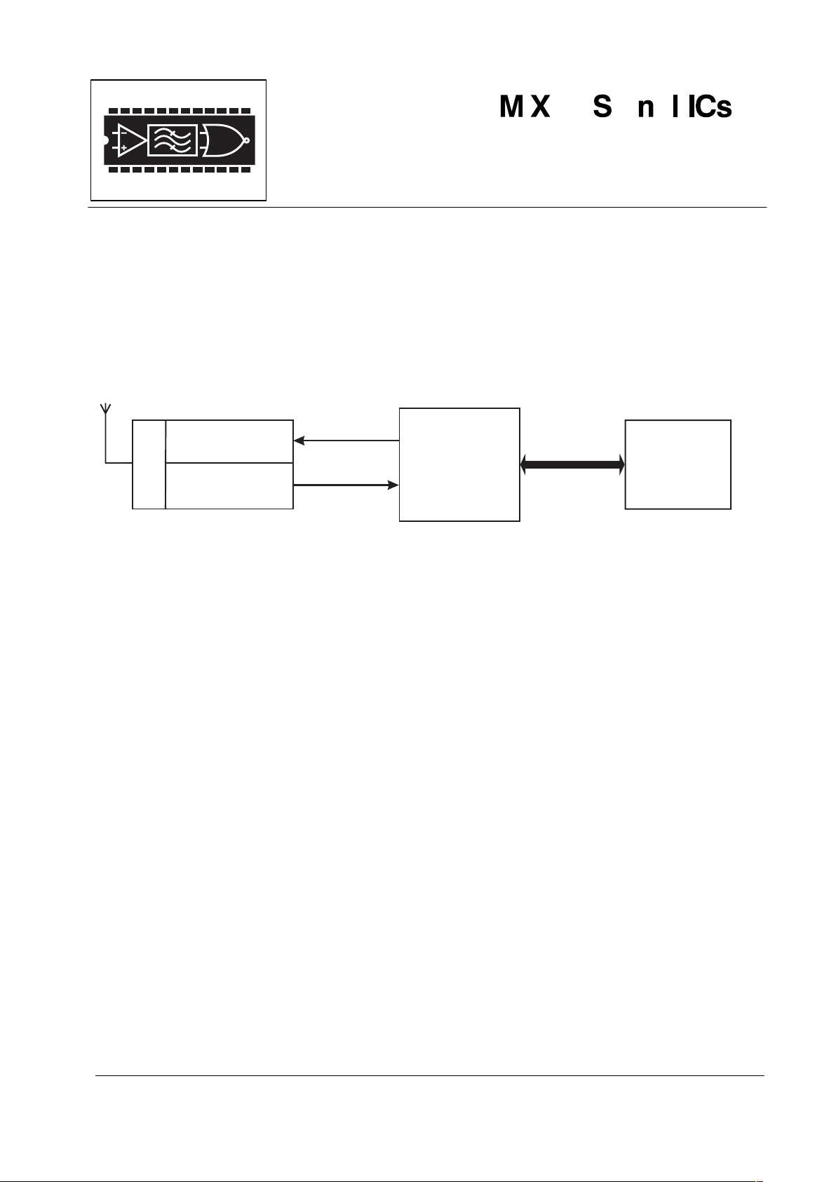
MODEM
DAT A
PUMP
MX909A
ANALOG TX
DATA AND
CONTROL BUS
ANALOG RX
RF
RADIO
DISCRIMINAT OR
MODULATOR
SYSTEM
APPLICATION
PROCESSING
HOST Cµ
The MX909A is a low power CMOS device containing all of the baseband signal processing and Medium
Access Control (MAC) protocol functions required for a high performance GMSK Wireless Packet Data
Modem. The MX909A interfaces with a host C and radio modulation/demodulation circuits to deliver reliable
two-way transfer of application data over a wireless link.
The MX909A assembles application data received from the host C, adds forward error correction (FEC), and
error detection (CRC) codes, time-spreads this data by interleaving (burst-error protection) and scrambles
(randomizes) the bit pattern. After automatically adding bit and frame sync codewords, the data packet is
converted into analog GMSK signals for modulating into the radio transmitter.
In the receive mode, the MX909A performs the reverse function using the analog signals from the receivers
discriminator. After error correction and removal of the packet overhead, the recovered application data is
supplied to the host C. Any CRC detected residual uncorrected errors in the data will be flagged. Readout
of the SNR value during receipt of a packet is also provided.
The MX909A uses data block sizes and FEC/CRC algorithms compatible with the Mobitex Wide Area
Network over-air standard. The format used is suitable for other private applications where the high-speed
transfer of data over narrow-band wireless links is required. The MX909A is programmable to operate at
standard bit-rates from a wide choice of XTAL/CLOCK frequencies.
The MX909A may be used with a 3.0V to 5.5V power supply and is available in the following packages:
24-pin SSOP (MX909ADS), 24-pin SOIC (MX909ADW), 24-pin PLCC (MX909ALH), and
24-pin PDIP (MX909AP).
Page 2

GMSK Modem Data Pump 2 MX909A PRELIMINARY INFORMATION
1998 MX-COM, Inc. www.mxcom.com Tel: 800 638 5577 336 744 5050 Fax: 336 744 5054 Doc. # 20480134.003
4800 Bethania Station Road, Winston-Salem, NC 27105-1201 USA All trademarks and service marks are held by their respective companies.
CONTENTS
Section Page
1 Block Diagram................................................................................................................3
2 Signal List.......................................................................................................................4
3 External Components....................................................................................................5
4 General Description.......................................................................................................6
4.1 Description of Data Blocks................................................................................................ 6
4.2 Modem - µC Interaction.................................................................................................... 9
4.3 Data Formats.................................................................................................................... 9
4.4 The Programmer's View................................................................................................. 11
4.5 CRC, FEC, Interleaving and Scrambling Information..................................................... 22
5 Application ...................................................................................................................25
5.1 Transmit Frame Example ............................................................................................... 25
5.2 Receive Frame Example ................................................................................................ 27
5.3 Clock Extraction and Level Measurement Systems ....................................................... 29
5.4 AC Coupling ................................................................................................................... 30
5.5 Radio Performance......................................................................................................... 32
6 Performance Specification..........................................................................................33
6.1 Electrical Performance ................................................................................................... 33
6.2 Packaging....................................................................................................................... 37
MXCOM, Inc. Reserves the right to change specifications at any time and without notice.
Page 3
GMSK Modem Data Pump 3 MX909A PRELIMINARY INFORMATION
1998 MX-COM, Inc. www.mxcom.com Tel: 800 638 5577 336 744 5050 Fax: 336 744 5054 Doc. # 20480134.003
4800 Bethania Station Road, Winston-Salem, NC 27105-1201 USA All trademarks and service marks are held by their respective companies.
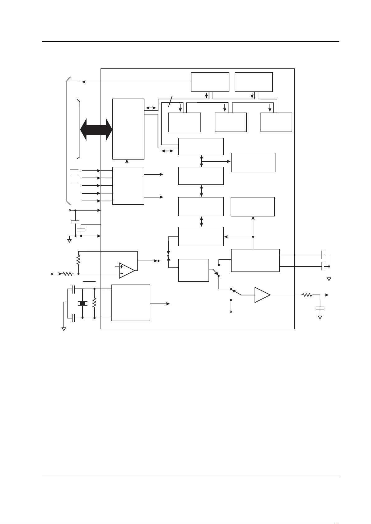
1 Block Diagram
V
SS
V
BIAS
XTAL /
CLOCK
TXOUT
RXIN
Rx Input Amp
Tx Output Buffer
DOC1
DOC2
D0
D1
D2
D3
D4
D5
D6
D7
A0
A1
8
Tx
Tx Bits
Rx Bits
Tx
Rx
Tx
Rx
Rx
V
BIAS
µCONTROLLER
INTERFACE
DATA
BUS
BUFFERS
ADDRESS
AND
R/W
DECODE
CRC
GENERATOR/
CHECKER
FRAME
SYNC DETECT
Rx LEVEL/CLOCK
EXTRACTION
FEC
GENERATOR/
CHECKER
INTERLEAVE/
DE-INTERLEAVE
SCRAMBLE/
DE-SCRAMBLE
CONTROL
REGISTER
MODE
REGISTER
COMMAND
REGISTER
DA T A
BUFFER
STA TUS
REGISTER
DATA
QUALITY
REGISTER
LOW PASS
FIL TER
CLOCK
OSCILLATOR
AND
DIVIDERS
RXAMPOUT
V
DD
XTAL
WR
RD
CS
IRQ
V
DD
V
BIAS
Figure 1: Block Diagram
Page 4

GMSK Modem Data Pump 4 MX909A PRELIMINARY INFORMATION
1998 MX-COM, Inc. www.mxcom.com Tel: 800 638 5577 336 744 5050 Fax: 336 744 5054 Doc. # 20480134.003
4800 Bethania Station Road, Winston-Salem, NC 27105-1201 USA All trademarks and service marks are held by their respective companies.
2 Signal List
Pin No Signal Type Description
1
IRQ
output
This pin is a ‘wire-ORable' output for connection to the host C's Interrupt
Request input. When active, this output has a low impedance pull down
to V
SS
. It has a high impedance when inactive.
2D7BUS
3D6BUS
4 D5 BUS Pins 2-9 (D7 - D0) are 8-bit, bi-directional, 3-state
5D4BUS
C interface data lines
6D3BUS
7D2BUS
8D1BUS
9D0BUS
10
RD
input Read. An active low logic level input used to control the reading of data
from the modem into the host C.
11
WR
input Write. An active low logic level input used to control the writing of data
into the modem from the host C.
12
V
SS
power Negative supply. (ground).
13
CS
input Chip Select. An active low logic level input to the modem. It is used to
enable a data read or write operation.
14 A0 input Logic level modem register select input.
15 A1 input Logic level modem register select input.
16
XTAL
output Output of the on-chip oscillator.
17 XTAL/CLOCK input Input to the on-chip oscillator, for an external CLOCK or XTAL circuit.
18 DOC 2 output Connects to the Rx level measurement circuitry. Should be capacitive
coupled to V
SS
.
19 DOC 1 output Connects to the Rx level measurement circuitry. Should be capacitive
coupled to V
SS.
20 TXOUT output Tx output signal from the modem.
21
V
BIAS
output
A bias line for the internal circuitry, held at V
DD
/2. This pin must be
bypassed to V
SS
by a capacitor mounted close to the device pins.
22 RXIN input Input to the Rx input amplifier.
23 RXAMPOUT output The output of the Rx input amplifier.
24
V
DD
power Positive supply. Voltage levels are dependent upon this supply. This pin
should be bypassed to V
SS
by a capacitor mounted close to the device
pins.
Page 5
GMSK Modem Data Pump 5 MX909A PRELIMINARY INFORMATION
1998 MX-COM, Inc. www.mxcom.com Tel: 800 638 5577 336 744 5050 Fax: 336 744 5054 Doc. # 20480134.003
4800 Bethania Station Road, Winston-Salem, NC 27105-1201 USA All trademarks and service marks are held by their respective companies.
3 External Components
DOC1
DOC2
V
DD
V
DD
V
SS
V
BIAS
RXIN
GMSKIN
GMSKOUT
RXAMPOUT
R2
R4
R1
µCONTROLLER INTERFACE
MX909A
TXOUT
C7
C5
C3
C4
R3
X1
C6
C1
C2
D7
D6
D5
D4
D3
D2
D1
D0
A0
A1
A1
A0
XTAL/CLOCK
XTAL/CLOCK
1
2
3
4
5
6
8
9
10
11
12
13
14
7
24
23
22
21
20
19
18
17
17
16
16
15
IRQ
XT AL
XT AL
RD
WR
CS
CS
Figure 2: Recommended External Components
Component Notes Value Tolerance
R1 1
20%
R2
100k
10%
R3
1M
20%
R4 2
5%
C1 0.1 µF
20%
C2 0.1 µF
20%
C3 3
20%
C4 3
20%
C5 2
10%
C6 4
20%
C7 4
20%
X1 3
Recommended External Component Notes:
1. See section 4.1.10.
2. See section 4.1.12.
3. See section 4.4.3.
4. C6 and C7 values should satisfy the following formula:
C (Farads) = 120 x 10-6 / Data Rate (bits/second)
Data Rate (kbits/sec) 4.0 4.8 8.0 9.6 16.0 19.2
C6 / C7 (uF) 0.03 0.022 0.015 0.012 0.0068 0.0068
Page 6
GMSK Modem Data Pump 6 MX909A PRELIMINARY INFORMATION
1998 MX-COM, Inc. www.mxcom.com Tel: 800 638 5577 336 744 5050 Fax: 336 744 5054 Doc. # 20480134.003
4800 Bethania Station Road, Winston-Salem, NC 27105-1201 USA All trademarks and service marks are held by their respective companies.
4 General Description
This product has been designed to be compliant with the appropriate sections of the “MobitexTM Interface
Specification”.
4.1 Description of Data Blocks
4.1.1 Data Bus Buffers
8 bi-directional, 3-state logic level buffers between the modem’s internal registers and the host C’s data bus
lines.
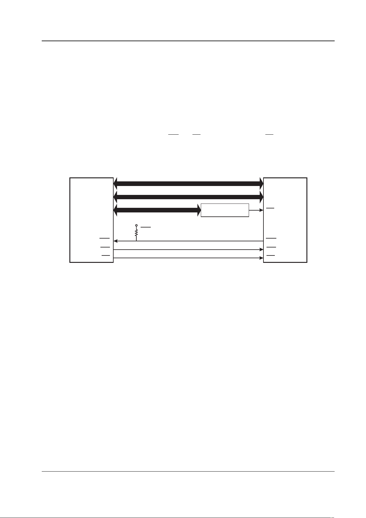
4.1.2 Address and R/W Decode
This block controls the transfer of data bytes between the C and the modem’s internal registers, according to
the state of the Write and Read Enable inputs (
WR and RD ), the Chip Select input CS), and the Register
Address inputs A0 and A1.
The Data Bus Buffers, Address, and R/W Decode blocks provide a byte-wide parallel C interface, which can
be memory mapped, as shown in Figure 3.
Address Bus
µC
MODEM
WR
RD
CS
RD
Address Decode
Circuit
Data Bus
IRQ
V
DD
D0:7
A0:1
WR
IRQ pull up
resistor
D0:7
IRQ
A2:7
A0:1
Figure 3: Typical Modem C Connections
4.1.3 Status and Data Quality Registers
8-bit registers which the µC can read to determine the status of the modem and the received data quality.
4.1.4 Command, Mode and Control Registers
The values written by the µC to these 8-bit registers control the operation of the modem.
4.1.5 Data Buffer
An 18-byte buffer used to hold receive or transmit data to or from the µC.
4.1.6 CRC Generator/Checker
A circuit which generates (in transmit mode) or checks (in receive mode) the Cyclic Redundancy Checksum
bits, which are included in transmitted Mobitex data blocks so the receive modem can detect transmission
errors.
4.1.7 FEC Generator/Checker
In transmit mode this circuit calculates and adds the Forward Error Correction (4 bits) to each byte presented
to it. In receive mode the FEC information is used to correct most transmission errors that have occurred in a
Mobitex Data Block or in the Frame Head control bytes.
4.1.8 Interleave / De-interleave Buffer
This circuit interleaves data bits within a data block before transmission and de-interleaves the received data
block so the FEC system is best able to handle short noise bursts or signal fades.
4.1.9 Frame Sync Detect
This circuit, (only active in receive mode), is used to look for the user specified 16-bit Frame Synchronization
pattern which is transmitted to mark the start of every frame.
Page 7

GMSK Modem Data Pump 7 MX909A PRELIMINARY INFORMATION
1998 MX-COM, Inc. www.mxcom.com Tel: 800 638 5577 336 744 5050 Fax: 336 744 5054 Doc. # 20480134.003
4800 Bethania Station Road, Winston-Salem, NC 27105-1201 USA All trademarks and service marks are held by their respective companies.
4.1.10 Rx Input Amp
This amplifier allows the received signal input to the modem to be set to the optimum level by suitable
selection of the external components R1 and R2. The value of R1 should be calculated to give (0.2 x V
DD)VP-
P
at the RXAMPOUT pin for a received '...11110000...' sequence.
A capacitor may be fitted if AC coupling of the received signal is desired (see section 5.4), otherwise the DC
level of the received signal should be adjusted so that the signal at the modem's RXAMPOUT pin is centered
around V
BIAS
(VDD/2).
4.1.11 Tx/Rx Low Pass Filter
This filter, which is used in both transmit and receive modes, is a low pass transitional Gaussian filter having a
loss of 3dB at 0.3 times the selected bit rate (BT = 0.3). See Figure 4.
In transmit mode, the bits are passed through this filter to eliminate the high frequency components which
would otherwise cause interference into adjacent radio channels.
In receive mode this filter is used with an increased BT factor (0.56) to reject HF noise, so the signal is
suitable for extraction of the received data.
4.1.12 Tx Output Buffer
This is a unity gain amplifier used in transmit mode to buffer the output of the Tx low pass filter. In receive
mode, the input of this buffer is connected to V
BIAS
. When changing from Rx to Tx mode the input to this
buffer will be connected to V
BIAS
for 2 bit periods to prevent unwanted signals, from the low pass filter, at the
output. When the modem is set to powersave mode, the buffer is turned off and the TXOUT pin connected to
V
BIAS
via a high value resistance. When exiting from power save mode the Tx output is only reconnected to
the buffer after 2 bit periods, to prevent unwanted signals, from the low pass filter, at the output.
Note: The RC low pass filter formed by the external components R4 and C5 between the Tx Output Buffer
and the input to the radio's frequency modulator forms an important part of the transmit signal filtering.
These components may form part of any DC level-shifting and gain adjustment circuitry. The ground
connection to the capacitor C5 should be positioned to give maximum attenuation of high frequency
noise into the modulator. R4 and C5 should be chosen so that the product of the resistance of R4 and
capacitance of C5 is 0.34/bit rate (bit rate in bits per second). R4 should be not less than 47k and the
value used for the external capacitor should take into account parasitic capacitance.
Suitable values being:
R4 C5
8000 bits/sec 100k
430pF
4800 bits/sec
100k
710pF
The signal at the TXOUT pin is centered around V
BIAS
and is approx. (0.2 x VDD)V
P-P
, going positive for a
logic '1' and negative for a logic '0', if the modem is not inverting the Tx data.
A capacitor may be fitted if AC coupling of the input to the frequency modulator is desired, see section 5.4.
The 'eye' diagram of the transmitted signal (after the external R4/C5 network) is shown in Figure 5.
Page 8

GMSK Modem Data Pump 8 MX909A PRELIMINARY INFORMATION
1998 MX-COM, Inc. www.mxcom.com Tel: 800 638 5577 336 744 5050 Fax: 336 744 5054 Doc. # 20480134.003
4800 Bethania Station Road, Winston-Salem, NC 27105-1201 USA All trademarks and service marks are held by their respective companies.
-80
-70
-60
-50
-40
-30
-20
-10
0
0 0.2 0.4 0.6 0.8 1 1.2 1.4 1.6 1.8 2
GAIN (dB)
FREQUENCY
DA T A RATE
Figure 4: Typical Tx Filter Frequency Response (after the external RC Filter)
012
Figure 5: Transmitted Eye Signal Diagram (after the external RC Filter)
4.1.13 Rx Level/Clock Extraction
These circuits, which operate only in receive mode, extract a bit rate clock from the received signal and
measure the received signal amplitude and DC offset. This information is then used to extract the received
bits and also to provide an input to the received Data Quality measuring circuit. The external capacitors C6
and C7 form part of the received signal level measuring circuit.
Page 9

GMSK Modem Data Pump 9 MX909A PRELIMINARY INFORMATION
1998 MX-COM, Inc. www.mxcom.com Tel: 800 638 5577 336 744 5050 Fax: 336 744 5054 Doc. # 20480134.003
4800 Bethania Station Road, Winston-Salem, NC 27105-1201 USA All trademarks and service marks are held by their respective companies.
4.1.14 Clock Oscillator and Dividers
This circuit derives the transmit bit rate (and the nominal receive bit rate) by frequency division of a reference
frequency which may be generated by the on-chip Xtal oscillator or applied from an external source.
Note: If the on-chip Xtal oscillator is to be used, then external components X1, C3, C4 and R3 are required.
If an external clock source is to be used, then the external clock source should be connected to the
XTAL/CLOCK input pin, the
XTALpin should be left unconnected, and X1, C3, C4, and R3 not fitted.
4.1.15 Scramble/De-scramble
This block may be used to scramble/de-scramble the transmitted/received data blocks. It does this by
modulating the data with a 511-bit pseudorandom sequence, as described in section 4.5.4, smoothes the
transmitted spectrum, especially when repetitive sequences are to be transmitted.
4.2 Modem - µC Interaction
In general, data is transmitted over air in the form of messages, or 'Frames', consisting of a 'Frame Head'
optionally followed by one or more formatted data blocks. The Frame Head includes a Frame
Synchronization pattern designed to allow the receiving modem to identify the start of a frame. The following
data blocks are constructed from the 'raw' data using a combination of CRC (Cyclic Redundancy Checksum)
generation, Forward Error Correction coding, Interleaving and Scrambling. Details of the message formats
handled by this modem are given in section 4.3.
To reduce the processing load on the host µC, this modem has been designed to perform as much as
possible of the computationally intensive work involved in Frame formatting / de-formatting and (when in
receive mode) in searching for and synchronizing onto the Frame Head. In normal operation the modem will
only require servicing by the µC once per received or transmitted data block.
Thus, to transmit a block, the host µC has only to load the unformatted (raw) binary data into the modem's
data buffer then instruct the modem to format and transmit that data. The modem will then calculate and add
the CRC bits as required, encode the result with Forward Error Correction coding, interleave then scramble
the bits before transmission.
In receive mode, the modem can be instructed to assemble a block's worth of received bits, de-scramble and
de-interleave the bits, check and correct them (using the FEC coding) and check the resulting CRC before
placing the received binary data into the Data Buffer for the µC to read.
The modem can also handle the transmission and reception of unformatted data, to allow the transmission of
special Bit and Frame Synchronization sequences or test patterns.
4.3 Data Formats
4.3.1 General Purpose Formats
In a proprietary system the user may employ the data elements provided by this device to construct a custom,
over-air data structure.
For example, 16 bits of bit sync + 2 bytes of frame sync + 4 bytes of receiver and sender address + n data
blocks would be: transmitted as:
TQB (bit and frame sync) + TQB (addresses) + (n x TDB) + TSB
received as:
SFS + RSB + RSB + RSB + RSB + (n x RDB)
Note: It is important to have established frame Synchronization before receiving data to enable the receiving
device to decode synchronously. The user may add, by way of algorithms performed on the controlling
device, additional data correction with the bytes in the data block task.
4.3.2 Mobitex Frame Structure
The Mobitex format for transmitted data is in the form of a Frame Head immediately followed by a number of
Data Blocks (0 to 32).
The Frame Head consists of 7 bytes:
2 bytes of bit sync:
1100110011001100 from base,
0011001100110011 from mobile
bits are transmitted from left to right
Page 10

GMSK Modem Data Pump 10 MX909A PRELIMINARY INFORMATION
1998 MX-COM, Inc. www.mxcom.com Tel: 800 638 5577 336 744 5050 Fax: 336 744 5054 Doc. # 20480134.003
4800 Bethania Station Road, Winston-Salem, NC 27105-1201 USA All trademarks and service marks are held by their respective companies.
Mobitex Frame Structure cont...
2 bytes of frame sync:
System specific.
2 bytes of control data.
1 byte of FEC code, 4 bits for each of the control bytes:
bits 7-4 (leftmost) operate on the first control byte.
bits 3-0 (rightmost) operate on the second control byte.
Each byte in the Frame Head is transmitted bit 7 (MSB) first to bit 0 (LSB) last.
The Data Block consists of:
18 bytes of data.
2 bytes of CRC calculated from the 18 data bytes.
4 bits of FEC code for each of the data and CRC bytes
The resulting 240 bits are interleaved and scrambled before transmission.
The over air signal is composed of Frame Sync and Bit Sync patterns, Control bytes, and Data Blocks as
shown in Figure 6.
The binary data transferred between the modem and the host µC is shown in the Frame Head and Data Block
of Figure 6 as shaded areas.
INTERLEAVING / DE-INTERLEAVING
SCRAMBLE / DESCRAMBLE
7654321
0
CRC (2 bytes)
loaded first
loaded last
4
5
6
7
8
9
0
1
2
3
18
19
14
15
16
17
10
11
12
13
FEC
LSB
MSB
321076543210
Frame H ead
MSB LSB
FEC2FEC1
Byte
loaded first
loaded last
1
2
4
3
5
6
Data Block
DB 0
DB n
DB 1
DB 2 DB 3 DB 4
FRAME
SYNC
16
16
8
FRAME HEAD
16
BITS
CTRL
BYTES
BIT
SYNC
FEC
DATA
BLOCKS
DAT A BLOCKS (0 to 32)
FRAME
OVER - AIR
SIGNAL
0
Byte
Data
(18 bytes)
Bit Sync 1
Bit Sync 2
Frame Sync 1
Frame Sync 2
Control Byte 1
Control Byte 2
Figure 6: Mobitex Over Air Signal Format
Page 11
GMSK Modem Data Pump 11 MX909A PRELIMINARY INFORMATION
1998 MX-COM, Inc. www.mxcom.com Tel: 800 638 5577 336 744 5050 Fax: 336 744 5054 Doc. # 20480134.003
4800 Bethania Station Road, Winston-Salem, NC 27105-1201 USA All trademarks and service marks are held by their respective companies.
4.4 The Programmer's View
The modem appears to the programmer as 4 write only 8-bit registers shadowed by 3 read only registers,
individual registers being selected by the A0 and A1 chip inputs:
A1 A0 Write to Modem Read from Modem
0 0 Data Buffer Data Buffer
0 1 Command Register Status Register
1 0 Control Register Data Quality Register
1 1 Mode Register not used
4.4.1 Data Buffer
This is an 18-byte read/write buffer which is used to transfer data (as opposed to command, status, mode,
data quality and control information) between the modem and the host µC.
It appears to the µC as a single 8-bit register; the modem ensuring that sequential µC reads or writes to the
buffer are routed to the correct locations within the buffer.
The µC should only access this buffer when the Status Register BFREE (Buffer Free) bit is '1'.
The buffer should only be written to while in Tx mode and read from while in Rx mode (except when loading
Frame Sync detection bytes while in Rx mode).
4.4.2 Command Register
Writing to this register tells the modem to perform a specific action or actions, depending on the setting of the
TASK, AQLEV and AQBC bits.
76543210
Command Register
AQBC AQLEV
Reserved
set to '0 0 0'
TASK
When there is no action to perform and not 'powersaved', the modem will be in an 'idle' state. If the modem is
in transmit mode the input to the Tx filter will be connected to V
BIAS
. In receive mode the modem will
continue to measure the received data quality and extract bits from the received signal, supplying them to the
de-interleave buffer, otherwise the received data is ignored.
4.4.2.1 Command Register B7: AQBC - Acquire Bit Clock
This bit has no effect in transmit mode.
In receive mode, when a byte with AQBC bit set to '1' is written to the Command Register, and TASK is not
set to RESET, it initiates an automatic sequence designed to achieve bit timing Synchronization with the
received signal as quickly as possible. This involves setting the Phase Locked Loop of the received bit timing
extraction circuits to its widest bandwidth, then gradually reducing the bandwidth as timing Synchronization is
achieved, until the 'normal' value set by the PLLBW bits of the Control Register is reached.
Setting this bit to '0' (or changing it from '1' to '0') has no effect, however note that the acquisition sequence
will be re-started every time that a byte written to the Command Register has the AQBC bit set to '1'.
The AQBC bit will normally be set up to 12 bits before an SFS (Search for Frame Sync) or SFH (Search for
Frame Head) task, however it may also be used independently to re-establish clock Synchronization quickly
after a long fade. Alternatively, an SFS or SFH task may be written to the Command Register with the AQBC
bit '0' if it is known that clock Synchronization does not need to be re-established. More details of the bit clock
acquisition sequence are given in section 5.3.
4.4.2.2 Command Register B6: AQLEV - Acquire Receive Signal Levels
This bit has no effect in transmit mode.
In receive mode, when a byte with AQLEV bit set to '1' is written to the Command Register and TASK is not
set to RESET, it initiates an automatic sequence designed to measure the amplitude and DC offset of the
received signal as rapidly as possible. This sequence involves setting the measurement circuits to respond
quickly at first, then
Page 12

GMSK Modem Data Pump 12 MX909A PRELIMINARY INFORMATION
1998 MX-COM, Inc. www.mxcom.com Tel: 800 638 5577 336 744 5050 Fax: 336 744 5054 Doc. # 20480134.003
4800 Bethania Station Road, Winston-Salem, NC 27105-1201 USA All trademarks and service marks are held by their respective companies.
Command Register B6: AQLEV - Acquire Receive Signal Levels (cont...)
gradually increasing their response time, thereby improving the measurement accuracy, until the 'normal'
value set by the LEVRES bits of the Control Register is reached.
Setting this bit to '0' (or changing it from '1' to '0') has no effect, however the acquisition sequence will be re-
started every time a byte written to the Command Register has the AQLEV bit set to '1'.
The AQLEV bit will normally be set up to 12 bits before an SFS (Search for Frame Sync) or SFH (Search for
Frame Head) task is initiated, however it may also be used independently to re-establish signal levels quickly
after a long fade. Alternatively, an SFS or SFH task may be written to the Command Register with the
AQLEV bit at '0' if it is known that there is no need to re-establish the received signal levels. Further
information of the level measurement acquisition sequence is provided in section 5.3.
The error rate is highest immediately after an AQBC and AQLEV sequence is triggered and rapidly reduces to
its static value soon after. These erroneous bits could incorrectly trigger the frame sync detection circuits. It
is suggested that an SFH or SFS task be set 12 bits after setting either of the AQLEV or AQBC sequences.
4.4.2.3 Command Register B5, B4, B3
These bits should be set to '0'.
4.4.2.4 Command Register B2, B1, B0: TASK - Task
Operations such as transmitting a data block are treated by the modem as 'tasks' and are initiated when the
µC writes a byte to the Command Register with the TASK bits set to anything other than the 'NULL' code.
The µC should not write a task (other than NULL or RESET) to the Command Register or write to or read
from the Data Buffer when the BFREE (Buffer Free) bit of the Status Register is '0'.
Different tasks apply in receive and transmit modes.
When the modem is in transmit mode, all tasks other than NULL, RESET and TSO instruct the modem to
transmit data from the Data Buffer, formatting it as required. For these tasks the µC should wait until the
BFREE (Buffer Free) bit of the Status Register is '1', before writing the data to the Data Buffer, then it should
write the desired task to the Command Register. If more than 1 byte needs to be written to the Data Buffer,
byte number 0 of the block should be written first.
Once the byte containing the desired task has been written to the Command Register, the modem will:
Set the BFREE (Buffer Free) bit of the Status Register to '0'.
Take the data from the Data Buffer as quickly as it can - transferring it to the Interleave Buffer for
eventual transmission. This operation will start immediately if the modem is 'idle' (i.e. not transmitting
data from a previous task), otherwise it will be delayed until there is sufficient room in the Interleave
Buffer.
Once all of the data has been transferred from the Data Buffer the modem will set the BFREE and
IRQ bits of the Status Register to '1', (causing the chip
IRQ
output to go low if the IRQEN bit of the
Mode Register has been set to '1') to tell the µC that it may write new data and the next task to the
modem.
In this way the µC can write a task and the associated data to the modem while the modem is still transmitting
the data from the previous task. See Figure 7.
When the modem is in receive mode, the µC should wait until the BFREE bit of the Status Register is '1', then
write the desired task to the Command Register.
Once the byte containing the desired task has been written to the Command Register, the modem will:
Set the BFREE bit of the Status Register to '0'.
Wait until enough received bits are in the De-interleave Buffer.
Decode them as needed, and transfer any resulting data to the Data Buffer
Then the modem will set the BFREE and IRQ bits of the Status Register to '1', (causing the
IRQ
output to go low if the IRQEN bit of the Mode Register has been set to '1') to tell the µC that it may
read from the Data Buffer and write the next task to the modem. If more than 1 byte is contained in
the Data Buffer, byte number '0' of the data will be read first.
In this way the µC can read data and write a new task to the modem while the received bits needed for this
new task are being stored in the De-interleave Buffer. See Figure 8.
The above is not true for loading the Frame Sync detection bytes (LFSB): the bytes to be compared with the
incoming data must be loaded prior to the task bits being written.
Detailed timings for the various tasks are given in Figure 9 and Figure 10.
Page 13

GMSK Modem Data Pump 13 MX909A PRELIMINARY INFORMATION
1998 MX-COM, Inc. www.mxcom.com Tel: 800 638 5577 336 744 5050 Fax: 336 744 5054 Doc. # 20480134.003
4800 Bethania Station Road, Winston-Salem, NC 27105-1201 USA All trademarks and service marks are held by their respective companies.
TXOUT Signal
from Task 1 fromTask 2
Task 1 data Task 2 data
Data from C to Data Bufferµ
Task and/or Commands from C
to Command Register
µ
Status Register IRQ Bit
Status Register BFREE Bit
IRQ Output (IRQEN = '1')
Figure 7: Transmit Process
RXIN Signa l
forTask 1 forTask 2
IRQ Output (IRQEN = '1')
Status Register IRQ Bit
Status Register BFREE Bit
T ask 1 T ask 2
T ask 1 data
Data from Data Buffer to Cµ
T ask from C
to Command Register
µ
Figure 8: Receive Process
Mobitex Modem Tasks
B2 B1 B0 Receive Mode Transmit Mode
0 0 0 NULL NULL
0 0 1 SFH Search for Frame Head T7H Transmit 7 byte Frame Head
0 1 0 R3H Read 3 byte Frame Head Reserved
0 1 1 RDB Read Data Block TDB Transmit Data Block
1 0 0 SFS Search for Frame Sync TQB Transmit 4 Bytes
1 0 1 RSB Read Single Byte TSB Transmit Single Byte
1 1 0 LFSB Load Frame Sync Bytes TSO Transmit Scrambler Output
1 1 1 RESET Cancel any current action RESET Cancel any current action
4.4.2.5 NULL - No effect
This task is provided so that a AQBC or AQLEV command can be initiated without loading a new task.
Page 14

GMSK Modem Data Pump 14 MX909A PRELIMINARY INFORMATION
1998 MX-COM, Inc. www.mxcom.com Tel: 800 638 5577 336 744 5050 Fax: 336 744 5054 Doc. # 20480134.003
4800 Bethania Station Road, Winston-Salem, NC 27105-1201 USA All trademarks and service marks are held by their respective companies.
4.4.2.6 SFH - Search for Frame Head
Causes the modem to search the received signal for a Frame Head. The Frame Head will consist of a 16-bit
Frame Sync followed by control data (see Figure 6). The search will continue until a Frame Head has been
found, or until the RESET task is loaded.
The search is carried out by first attempting to match the incoming bits against the previously programmed
(task LFSB) 16-bit Frame Sync pattern (allowing up to any one bit (of 16) in error). When a match has been
found, the modem will read the next 3 received bytes as Frame Head bytes, these bytes will be checked, and
corrected if necessary, using the FEC bits. The two Frame Head Data bytes are then placed into the Data
Buffer.
The BFREE and IRQ bits of the Status Register will then be set to a logic '1' to indicate that the µC may read
the 2 Frame Head Data bytes from the Data Buffer and write the next task to the Command Register. If the
FEC indicates uncorrectable errors the modem will set the CRCFEC bit in the Status Register to a logic '1'.
The
MO BA/ bit (Mobile or Base) in the Status Register will be set according to the polarity of the 3 bits
preceding the Frame Sync pattern.
4.4.2.7 R3H - Read 3-byte Frame Head
This task, which would normally follow an SFS task, will place the next 3 bytes directly into the Data Buffer. It
also causes the modem to check the 3 bytes as Frame Head control data bytes and will set the CRCFEC bit
to a logic '1' only if the FEC bits indicate uncorrectable errors.
Note: This task will not correct any errors and, due to the Mobitex FEC specification, will not detect all
possible uncorrectable error patterns. The BFREE and IRQ bits of the Status Register will be set to '1'
when the task is complete to indicate that the µC may read the data from the Data Buffer and write the
next task to the modem's Command Register.
The CRCFEC bit in the Status Register will be set according to the validity of the received FEC bits.
4.4.2.8 RDB - Read Data Block
This task causes the modem to read the next 240 bits as a Mobitex Data Block.
It will de-scramble and de-interleave the bits, FEC correct and CRC check the resulting 18 data bytes and
place them into the Data Buffer, setting the BFREE and IRQ bits of the Status Register to '1' when the task is
complete to indicate that the µC may read the data from the Data Buffer and write the next task to the
modem's Command Register. The CRCFEC bit will be set according to the outcome of the CRC check.
Note: In receive mode the CRC checksum circuits are initialized on completion of any task other than NULL.
4.4.2.9 SFS - Search for Frame Sync
This task, which is intended for special test and channel monitoring purposes, performs the first part only of a
SFH task. It causes the modem to search the received signal for a 16-bit sequence which matches the
Frame Synchronization pattern with up to any 1 bit in error.
When a match is found the modem will set the BFREE and IRQ bits of the Status Register to '1' and update
the
MO BA/
bit. The µC may then write the next task to the Command Register.
4.4.2.10 RSB - Read Single Byte
This task causes the modem to read the next 8 bits and translate them directly (without de-interleaving or
FEC) to an 8-bit byte which is placed into the Data Buffer (B7 will represent the earliest bit received). The
BFREE and IRQ bits of the Status Register will then be set to '1' to indicate that the µC may read the data
byte from the Data Buffer and write the next task to the Command Register.
This task is intended for special tests and channel monitoring - perhaps preceded by an SFS task.
4.4.2.11 LFSB - Load Frame Sync Bytes
This task takes 2 bytes from the Data Buffer and updates the Frame Sync detect bytes. The MSB of byte '0'
is compared to the first bit of a received Frame Sync pattern and the LSB of byte '1' is compared to the last bit
of a received Frame Sync pattern. This task does not enable Frame Sync detection.
Unlike other Rx tasks, the data buffer must be loaded before the task is issued and the task must only be
issued 'between' received messages, i.e. before the first task for receiving a message and after the last data
is read out of the data buffer.
Once the modem has read the Frame Sync bytes from the Data Buffer, the BFREE and IRQ bits of the Status
Register will be set to '1', indicating to the µC that it may write the next task to the modem.
Page 15

GMSK Modem Data Pump 15 MX909A PRELIMINARY INFORMATION
1998 MX-COM, Inc. www.mxcom.com Tel: 800 638 5577 336 744 5050 Fax: 336 744 5054 Doc. # 20480134.003
4800 Bethania Station Road, Winston-Salem, NC 27105-1201 USA All trademarks and service marks are held by their respective companies.
4.4.2.12 T7H - Transmit 7-byte Frame Head
This task takes 6 bytes of data from the Data Buffer, calculates and appends 8 bits of FEC from bytes '4' and
'5' then transmits the result as a complete Mobitex Frame Head.
Bytes '0' and '1' form the bit sync pattern, bytes '2' and '3' form the frame sync pattern and bytes '4' and '5' are
the frame head control bytes. Bit 7 of byte '0' of the Data Buffer is sent first, bit 0 of the FEC byte last.
Once the modem has read the data bytes from the Data Buffer, the BFREE and IRQ bits of the Status
Register will be set to '1', indicating to the µC that it may write the next task and its data to the modem.
4.4.2.13 TQB - Transmit 4 Bytes
This task takes 4 bytes of data from the Data Buffer and transmits them, bit 7 first.
Once the modem has read the data bytes from the Data Buffer, the BFREE and IRQ bits of the Status
Register will be set to '1', indicating to the µC that it may write the next task and its data to the modem.
4.4.2.14 TDB - Transmit Data Block
This task takes 18 bytes of data from the Data Buffer, calculates and applies a 16-bit CRC and forms the FEC
for the 18 data bytes and the CRC. This data is then interleaved and passed through the scrambler, if
enabled, before being transmitted as a Mobitex Data Block.
Once the modem has read the data bytes from the Data Buffer, the BFREE and IRQ bits of the Status
Register will be set to '1', indicating to the µC that it may write the next task and its data to the modem.
Note: In transmit mode the CRC checksum circuit is initialized on completion of any task other than NULL.
4.4.2.15 TSB - Transmit Single Byte
This task takes a byte from the Data Buffer and transmits the 8 bits, bit 7 first.
Once the modem has read the data byte from the Data Buffer, the BFREE and IRQ bits of the Status Register
will be set to '1', indicating to the µC that it may write the next task and its data to the modem.
4.4.2.16 TSO - Transmit Scrambler Output
This task, intended for channel set-up, enables the scrambler and transmits its output.
When the modem has started the task, the Status Register bits will not be changed and an IRQ will not be
raised. The µC may write the next task and its data to the modem at any time and the scrambler output will
stop when the new task has produced its first data.
4.4.2.17 RESET - Stop any current action
This task takes effect immediately, and terminates any current action (task, AQBC or AQLEV) the modem
may be performing and sets the BFREE bit of the Status Register to '1', without setting the IRQ bit. It should
be used when V
DD
is applied to set the modem into a known state.
Note: Due to delays in the internal switched capacitor filter, it will take approximately 3 bit times for any
change to become apparent at the TXOUT pin.
4.4.2.18 Task Timings
The device should not be given a new task for at least 2 bit times after the following:
Changing from powersave state to normal operation.
Changing the
Tx Rx/ bit.
Resetting or after power is applied to the device.
This is to ensure that the internal operation of the device is initialized correctly for the new task.
Note: This only applies to the Command Register, other registers may be accessed as normal.
Page 16

GMSK Modem Data Pump 16 MX909A PRELIMINARY INFORMATION
1998 MX-COM, Inc. www.mxcom.com Tel: 800 638 5577 336 744 5050 Fax: 336 744 5054 Doc. # 20480134.003
4800 Bethania Station Road, Winston-Salem, NC 27105-1201 USA All trademarks and service marks are held by their respective companies.
Ref. Figure 9 and Figure 10 Task Typical (bit-times)
t
1
Time from writing first task (modem in 'idle' state) to
application of first transmit bit to Tx Low Pass filter
Any 1
t
2
Time from application of first bit of task to TX Low
Pass Filter until BFREE goes to a logic 1
T7H
TQB
TDB
TSB
36
24
20
1
t
3
Time to transmit all bits of task T7H
TQB
TDB
TSB
56
32
240
8
t
4
Max time allowed from BFREE going to a logic 1 for
next task (and data) to be written to the modem
T7H
TQB
TDB
TSB
18
6
218
6
t
5
Time to receive all bits of task SFH
R3H
RDB
RSB
56
24
240
8
t
6
Maximum time between first bit of task entering
de-interleave circuit and task being written to modem
SFH
R3H
RDB
RSB
14
18
218
6
t
7
Time from last bit of task entering de-interleave
circuit to BFREE going to a logic '1'
Any 1
from Task 2
from Task 3
from Task 1
t
1
t
2
Task to Command Register
Data to Data B u ffer
t
3
t
4
ModemTx Output
12
1 2
Bits toTx Low p as s F ilte r
3
IBEMPTY Bit
BFREE Bit
3
t
2
t
2
t
3
t
3
t
4
t
4
Figure 9: Transmit Mode Timing Diagram
Page 17

GMSK Modem Data Pump 17 MX909A PRELIMINARY INFORMATION
1998 MX-COM, Inc. www.mxcom.com Tel: 800 638 5577 336 744 5050 Fax: 336 744 5054 Doc. # 20480134.003
4800 Bethania Station Road, Winston-Salem, NC 27105-1201 USA All trademarks and service marks are held by their respective companies.
forTask 2 for Task 3forTask 1
Task to Command Register
Data from Data Buffer
Modem Rx Input
12
1
2
Bits to De-Interleave Circuit
3
BFREE Bit
3
t
5
t
6
t
7
t
5
t5t
5
t
6
t
6
t
7
t
7
Figure 10: Receive Mode Timing Diagram
4.4.2.19 Tx/Rx Low Pass Filter Delay
The previous task timing figures are based on the signal at the input to the Tx Low Pass filter (in transmit
mode) or the input to the de-interleave buffer (in receive mode). There is an additional delay of about 2 bit
times in both transmit and receive modes due to the Tx/Rx Low Pass filter, as illustrated in Figure 11.
Tx bit to Low Pass Filter
Tx bit afterTx RC N etwork / Rx bit from FM Disc rimin a to r
Bit from Rx Extraction Circuit
Bit times
Figure 11: Low Pass Filter Delay
4.4.3 Control Register
This 8-bit write only register controls the modem's bit rate, the response times of the receive clock extraction
and signal level measurement circuits and the internal analog filters.
76543210
Control Register
CKDIV
HI/LO
DARA
LEVRES PLLBW
Page 18

GMSK Modem Data Pump 18 MX909A PRELIMINARY INFORMATION
1998 MX-COM, Inc. www.mxcom.com Tel: 800 638 5577 336 744 5050 Fax: 336 744 5054 Doc. # 20480134.003
4800 Bethania Station Road, Winston-Salem, NC 27105-1201 USA All trademarks and service marks are held by their respective companies.
4.4.3.1 Control Register B7, B6: CKDIV - Clock Division Ratio and B5:
HI/LO
- Xtal Range Selection
These bits control a frequency divider driven from the clock signal present at the
XTAL pin, which determines
the nominal bit rate. The table below shows how bit rates of 4000/8000/16000 or 4800/9600/19200 bits/sec
may be obtained from common Xtal frequencies:
B5 XTAL / CLOCK Frequency (MHz)
1 8.192 9.8304 4.096
(12.288/3)
4.9152 2.048
(6.144/3)
2.4576
(12.288/5)
0 4.096
(12.288/3)
4.9152 2.048
(6.144/3)
2.4576
(12.288/5)
1.024 1.2288
B7 B6
Division Ratio:
XTAL Frequency
Data Rate
Data Rates (bits per second)
0 0 256 128 16000 19200 8000 96000
0 1 512 256 16000 19200 8000 9600 4000 4800
1 0 1024 512 8000 9600 4000 4800
1 1 2048 1024 4000 4800
Note: Device operation is not guaranteed below 4000 or above 19200 bits/sec.
The values used for C3 and C4 should be suitable for the frequency of the crystal X1. As a guide; C3 = C4 =
33pF for X1 < 5MHz, and C3 = C4 = 18pF for X1 > 5MHz.
4.4.3.2 Control Register B4: DARA - Data Rate
This bit operates in both transmit and receive modes, optimizing the modem's internal signal filtering
according to the relevant bit rate.
If the bit rate used is above 10k bits/sec then this bit should be set to '1' , if not, then it should be set to '0'.
4.4.3.3 Control Register B3, B2: LEVRES - Level Measurement Response Time
These two bits have no effect in transmit mode.
In receive mode, they set the 'normal' response time of the Rx signal amplitude and DC offset measuring
circuits. This setting will be temporarily overridden by the automatic sequencing of an AQLEV command.
B3 B2
0 0 Hold Keep current values of amplitude and offset
0 1 Peak Averaging Track input signal using bit peak averaging
1 0 Peak Detect Track input signal using peak detect
1 1 Lossy Peak Detect Track input signal using lossy peak detection
For Mobitex systems, and most general purpose applications using the modem, these bits should normally
be set to 'Peak Averaging', except when the µC detects a receive signal fade, when 'Hold' should be selected.
The 'Lossy Peak Detect' setting is intended for systems where the µC cannot detect signal fades or the start
of a received message, as it allows the modem to respond quickly to fresh messages and recover rapidly
after a fade without µC intervention - although at the cost of reduced Bit Error Rate versus Signal to Noise
performance.
Note: Since the measured levels are stored on the external capacitors C6 and C7, they will decay gradually
towards V
BIAS
when the 'Hold' setting is chosen, the discharge time-constant being approximately 2000
bit times. Further information of the level measurement system is provided in section 5.3.
4.4.3.4 Control Register B1, B0: PLLBW
These two bits have no effect in transmit mode.
In receive mode, they set the 'normal' bandwidth of the Rx clock extraction Phase Locked Loop circuit. This
setting will be temporarily overridden by the automatic sequencing of an AQBC command.
Page 19

GMSK Modem Data Pump 19 MX909A PRELIMINARY INFORMATION
1998 MX-COM, Inc. www.mxcom.com Tel: 800 638 5577 336 744 5050 Fax: 336 744 5054 Doc. # 20480134.003
4800 Bethania Station Road, Winston-Salem, NC 27105-1201 USA All trademarks and service marks are held by their respective companies.
B1 B0 PLL Bandwidth Suggested use
0 0 Hold Signal fades
0 1 Narrow ± 20ppm or better Xtals
1 0 Medium Wide tolerance Xtals or long preamble acquisition
1 1 Wide Quick acquisition
The 'hold' setting is intended for use during signal fades, otherwise the minimum bandwidth consistent with
the transmit and receive modem bit rate tolerances should be chosen.
The wide and medium bandwidth settings are intended for systems where the µC cannot detect signal fades
or the start of a received message, as they allow the modem to respond rapidly to fresh messages and
recover rapidly after a fade without µC intervention - although at the cost of reduced Bit Error Rate versus
Signal to Noise performance.
Note: Further information of the clock extraction system is provided in section 5.3.
4.4.4 Mode Register
The contents of this 8-bit write only register control the basic operating modes of the modem:
76543210
Mode Register
IRQEN SCREN DQEN
INVBIT Reserved
set to '0 0'
Tx/Rx
PSAVE
4.4.4.1 Mode Register B7: IRQEN-
IRQ
Output Enable
When this bit is set to '1', the
IRQ
chip output pin is pulled low (to VSS) whenever the IRQ bit of the Status
Register is a '1'.
4.4.4.2 Mode Register B6: INVBIT - Invert Bits
This bit controls inversion of transmitted and received bit voltages. When set to '1' all data is inverted in the
Tx and Rx data paths so a transmitted '1' is a voltage below V
BIAS
at the TXOUT pin and a received '0' is a
voltage above V
BIAS
at the RXIN pin. Data will be inverted immediately after this bit is set to '1'.
4.4.4.3 Mode Register B5:
TX/RX - Tx/Rx Mode
Setting this bit to '1' puts the modem into Transmit mode, clearing it to '0' puts the modem into Receive mode.
When changing from Rx to Tx there must be a 2-bit pause before setting a new task to allow the filter to
stabilize. (See also PSAVE bit).
Note: Changing between receive and transmit modes will cancel any current task
4.4.4.4 Mode Register B4: SCREN - Scramble Enable
The scrambler only takes effect during the transmission or reception of a Mobitex Data Block and during a
TSO task. Setting this bit to '1' enables scrambling, clearing it to '0' disables scrambling.
The scrambler is only operative, if enabled by this control bit, during TSO, RDB or TDB, it is held in a reset
state at all other times.
This bit should not be changed while the modem is decoding or transmitting a Mobitex Data Block.
4.4.4.5 Mode Register B3: PSAVE - Powersave
When this bit is a '1', the modem will be in a 'powersave' mode in which the internal filters, the Rx bit and
Clock extraction circuits and the Tx output buffer will be disabled, and the TXOUT pin will be connected to
V
BIAS
through a high value resistance. The Xtal Clock oscillator and the µC interface logic will continue to
operate.
Setting the PSAVE bit to '0' restores power to all of the chip circuitry.
Note: The internal filters will take approximately 2 bit times to settle after the PSAVE bit is taken from '1' to '0'.
4.4.4.6 Mode Register B2: DQEN - Data Quality IRQ Enable
In receive mode, setting this bit to '1' causes the IRQ bit of the Status Register to be set to '1' whenever a new
Data Quality reading is ready. (The DQRDY bit of the Status Register will also be set to '1' at the same time.)
In transmit mode this bit has no effect.
Page 20

GMSK Modem Data Pump 20 MX909A PRELIMINARY INFORMATION
1998 MX-COM, Inc. www.mxcom.com Tel: 800 638 5577 336 744 5050 Fax: 336 744 5054 Doc. # 20480134.003
4800 Bethania Station Road, Winston-Salem, NC 27105-1201 USA All trademarks and service marks are held by their respective companies.
4.4.4.7 Mode Register B1, B0
These bits should be set to '0'.
4.4.5 Status Register
This register may be read by the µC to determine the current state of the modem.
76543210
Status Register
CRCFEC MO/BA
IRQ
DIBOVF
DQRDY
Reserved
BFREE
IBEMPTY
4.4.5.1 Status Register B7: IRQ - Interrupt Request
This bit is set to '1' by:
The Status Register BFREE bit going from '0' to '1', unless this is caused by a RESET task or by a
change to the Mode Register PSAVE or
TX RX/ bits.
The Status Register IBEMPTY bit going from '0' to '1', unless this is caused by a RESET task or by
changing the Mode Register PSAVE or
TX RX/ bits.
The Status Register DQRDY bit going from '0' to '1' (If DQEN = '1' ).
The Status Register DIBOVF bit going from '0' to '1'.
The IRQ bit is cleared to '0' immediately after a read of the Status Register.
If the IRQEN bit of the Mode Register is '1', then the chip
IRQ
output will be pulled low (to VSS) whenever the
IRQ bit is '1'.
4.4.5.2 Status Register B6: BFREE - Data Buffer Free
This bit reflects the availability of the Data Buffer and is cleared to '0' whenever a task other than NULL,
RESET or TSO is written to the Command Register.
In transmit mode, the BFREE bit will be set to '1' (also setting the Status Register IRQ bit to '1') by the modem
when the modem is ready for the µC to write new data to the Data Buffer and the next task to the Command
Register.
In receive mode, the BFREE bit is set to '1' (also setting the Status Register IRQ bit to '1') by the modem
when it has completed a task and any data associated with that task has been placed into the Data Buffer.
The µC may then read that data and write the next task to the Command Register.
The BFREE bit is also set to '1', but without setting the IRQ bit, by a RESET task or when the Mode Register
PSAVE or
TX RX/ bits are changed.
4.4.5.3 Status Register B5: IBEMPTY - Interleave Buffer Empty
In transmit mode, this bit will be set to '1', also setting the IRQ bit, when less than two bits remain in the
Interleave Buffer. Any transmit task written to the modem after this bit goes to '1' will be too late to avoid a
gap in the transmit output signal.
The bit is also set to '1' by a RESET task or by a change of the Mode Register
TX RX/ or PSAVE bits, but in
these cases the IRQ bit will not be set.
The bit is cleared to '0' by writing a task other than NULL, RESET or TSO to the Command Register.
Note: When the modem is in transmit mode and the Interleave Buffer is empty, a mid-level voltage (V
BIAS
)
will be applied to the Tx low pass filter.
In receive mode this bit will be '0'.
4.4.5.4 Status Register B4: DIBOVF - De-Interleave Buffer Overflow
In receive mode this bit will be set to '1' (also setting the IRQ bit) when a task is written to the Command
Register too late to allow continuous reception.
The bit is cleared to '0' by reading the Status Register or by writing a RESET task to the Command Register
or by changing the PSAVE or
TX RX/ bits of the Mode Register.
In transmit mode this bit will be '0'.
Page 21

GMSK Modem Data Pump 21 MX909A PRELIMINARY INFORMATION
1998 MX-COM, Inc. www.mxcom.com Tel: 800 638 5577 336 744 5050 Fax: 336 744 5054 Doc. # 20480134.003
4800 Bethania Station Road, Winston-Salem, NC 27105-1201 USA All trademarks and service marks are held by their respective companies.
4.4.5.5 Status Register B3: CRCFEC - CRC or FEC Error
In receive mode this bit will be updated at the end of a Mobitex Data Block task, after checking the CRC,
and at the end of receiving Frame Head control bytes, after checking the FEC. A '0' indicates that the CRC
was received correctly or the FEC did not find uncorrectable errors, a '1' indicates that errors are present.
The bit is cleared to '0' by a RESET task or by changing the PSAVE or
TX RX/ bits of the Mode Register.
In transmit mode this bit will be '0'.
4.4.5.6 Status Register B2: DQRDY - Data Quality Reading Ready
In receive mode, this bit is set to '1' whenever a Data Quality reading has been completed. See section 4.4.6.
The bit is cleared to '0' by a read of the Data Quality Register.
Immediately after a RESET task, or a change in the PSAVE or
TX RX/ bits to '0', the DQRDY bit may be set
and generate an interrupt. The value in the Data Quality Register will not be valid in this case.
4.4.5.7 Status Register B1:
MO/BA - Mobile or Base Bit Sync Received
In receive mode this bit is updated at the end of the SFS and SFH tasks. This bit is set to '1' whenever the 3
bits immediately preceding a detected Frame sync are '011' (received left to right), with up to any one bit in
error. The bit is set to '0' if the bit pattern is '100', again with up to any one bit in error. Thus, if this bit is set
to '1' then the received message is likely to have originated from a Mobile and if it is set to '0' from a Base
Station. See section 4.3.
In transmit mode this bit is a logic '0'.
4.4.5.8 Status Register B0
This bit will always be set to '0'.
4.4.6 Data Quality Register
This is intended to indicate the quality of the receive signal during a Mobitex Data Block or 30 single bytes.
In receive mode, the modem measures the 'quality' of the received signal by comparing the actual received
zero crossing time against an internally generated time. This value is averaged over 240 bits and at the end
of the measurement the Data Quality Register and the DQRDY bit in the Status Register is updated.
Note: An interrupt will only occur at this time if the DQEN bit = '1'.
To provide Synchronization with Data Blocks, and to ensure the Data Quality Register is updated in
preparation to be read when the RDB task finishes, the measurement process is reset at the end of tasks
SFH, SFS, RDB and R3H.
In transmit mode all bits of the Data Quality Register will be '0'.
Figure 12 shows how the value (0-240) read from the Data Quality Register varies with received signal to
noise ratio.
Page 22

GMSK Modem Data Pump 22 MX909A PRELIMINARY INFORMATION
1998 MX-COM, Inc. www.mxcom.com Tel: 800 638 5577 336 744 5050 Fax: 336 744 5054 Doc. # 20480134.003
4800 Bethania Station Road, Winston-Salem, NC 27105-1201 USA All trademarks and service marks are held by their respective companies.
0
20
40
60
80
100
120
140
160
180
200
220
240
34
5
678910
11 12
Received Signal-to-Noise Ratio (dB)
Data Quality Register Reading
Figure 12: Typical Data Quality Reading (after 240 bits) vs. S/N, (noise in bit rate bandwidth)
4.5 CRC, FEC, Interleaving and Scrambling Information
4.5.1 CRC
This is a 16-bit CRC code used in the Mobitex Data Block. In transmit it is calculated by the modem from
the 18 data bytes using the following generator polynomial:
g(x) = x16 + x12 + x5 + 1
i.e. CRC - CCITT X.25.
This code detects all (single) error bursts of up to 16 bits in length and about 99.998% of all other error
patterns.
The CRC register is initialized to all '1s' and the CRC is calculated octet by octet starting with the least
significant bit of 'byte 0'. The CRC calculated is bit-wise inverted and appended to the data bytes with the
most significant bit transmitted earliest.
In receive mode, a 16-bit CRC code is generated from the 18 data bytes of each Mobitex Data Block as
above and the bit-wise inverted value is compared with the received CRC bytes. If a mismatch is present,
then an error has been detected.
Page 23

GMSK Modem Data Pump 23 MX909A PRELIMINARY INFORMATION
1998 MX-COM, Inc. www.mxcom.com Tel: 800 638 5577 336 744 5050 Fax: 336 744 5054 Doc. # 20480134.003
4800 Bethania Station Road, Winston-Salem, NC 27105-1201 USA All trademarks and service marks are held by their respective companies.
4.5.2 FEC
In transmit mode, during T7H and TDB, the modem generates a 4-bit Forward Error Correction code for each
coded byte. The FEC is defined by the following H matrix:
7_______0 3___0
11101100 1000
H = 11010011 0100
10111010 0010
01110101 0001
Generation of the FEC consists of logically ANDing the byte to be transmitted with bits 7 to 0 of each row of
the H matrix. Even parity is generated for each of the 4 results and these 4 parity bits, in the positions
indicated by the last 4 columns of the H matrix, form the FEC code.
In checking the FEC, the received 12-bit word is logically ANDed with each row of the H matrix (earliest bit
received compared with the first column). Again even parity is generated for the 4 resulting words and these
parity bits form a 4-bit nibble. If this nibble is all zero then no errors have been detected. Other results 'point'
to the bit in error or indicate that uncorrectable errors have occurred.
This code can correct any single error that has occurred in each 12-bit (8 data + 4 FEC) section of the
message.
Example:
If the byte to be coded is '00101100' then the FEC is derived as follows:
H matrix row:1234
A 11101100 11010011 10111010 01110101
B 00101100 00101100 00101100 00101100
A AND B 00101100 00000000 00101000 00100100
Even Parity: 1000
Where A is bits 7 - 0 of one row of the H matrix and B is the byte to be coded. The even parity bits apply to
the result of 'A AND B'.
So the word formed will be: '00101100 1000' sent left to right
When the same process is carried out on these 12 bits as above, using all 12 bits of each H matrix row, the
resulting 4 parity bits will be '0000'.
4.5.3 Interleaving
The 240 bits of a Mobitex Data Block are interleaved by the modem before transmission to give protection
against noise bursts and short fades. Interleaving is not performed on any bits in the Mobitex Frame Head.
Considering the 240 bits to be numbered sequentially before interleaving as 0 to 239
('0' = bit 7 of byte 0, '11' = bit 0 of FEC for byte 0, ... ,'239' = bit 0 of FEC for byte 19 - see Figure 6), then they
will be transmitted as shown in Figure 13.
The modem performs the inverse operation (de-interleaving) in receive mode on Mobitex Data Blocks.
Page 24

GMSK Modem Data Pump 24 MX909A PRELIMINARY INFORMATION
1998 MX-COM, Inc. www.mxcom.com Tel: 800 638 5577 336 744 5050 Fax: 336 744 5054 Doc. # 20480134.003
4800 Bethania Station Road, Winston-Salem, NC 27105-1201 USA All trademarks and service marks are held by their respective companies.
0
12
24
36
48
60
72
84
96
108
120
132
144
156
168
180
192
204
216
228
7
INPUT DATA
INTERLEAVED OUTPUTTO
LOW PASS FILTER
DAT A BLOCK
1
13
25
37
49
61
73
85
97
109
121
133
145
157
169
181
193
205
217
229
6
2
14
26
38
50
62
74
86
98
110
122
134
146
158
170
182
194
206
218
230
5
3
15
27
39
51
63
75
87
99
111
123
135
147
159
171
183
195
207
219
231
4
4
16
28
40
52
64
76
88
100
112
124
136
148
160
172
184
196
208
220
232
3
5
17
29
41
53
65
77
89
101
113
125
137
149
161
173
185
197
209
221
233
2
6
18
30
42
54
66
78
90
102
114
126
138
150
162
174
186
198
210
222
234
1
7
19
31
43
55
67
79
91
103
115
127
139
151
163
175
187
199
211
223
235
0
8
20
32
44
56
68
80
92
104
116
128
140
152
164
176
188
200
212
224
236
3
9
21
33
45
57
69
81
93
105
117
129
141
153
165
177
189
201
213
225
237
2
10
22
34
46
58
70
82
94
106
118
130
142
154
166
178
190
202
214
226
238
01
11
23
35
47
59
71
83
95
107
119
131
143
155
167
179
191
203
215
227
239
0
1
2
3
4
5
6
7
8
9
10
11
12
13
14
15
16
17
18
19
CRC
CRC
loaded first
loaded last
0
12
24
36
48
60
72
84
96
108
120
132
144
156
168
180
192
204
216
228
1
13
25
37
49
61
73
85
97
109
121
133
145
157
169
181
193
205
217
229
2
14
26
38
50
62
74
86
98
110
122
134
146
158
170
182
194
206
218
230
3
15
27
39
51
63
75
87
99
111
123
135
147
159
171
183
195
207
219
231
4
16
28
40
52
64
76
88
100
112
124
136
148
160
172
184
196
208
220
232
5
17
29
41
53
65
77
89
101
113
125
137
149
161
173
185
197
209
221
233
6
18
30
42
54
66
78
90
102
114
126
138
150
162
174
186
198
210
222
234
7
19
31
43
55
67
79
91
103
115
127
139
151
163
175
187
199
211
223
235
8
20
32
44
56
68
80
92
104
116
128
140
152
164
176
188
200
212
224
236
9
21
33
45
57
69
81
93
105
117
129
141
153
165
177
189
201
213
225
237
10
22
34
46
58
70
82
94
106
118
130
142
154
166
178
190
202
214
226
238
11
23
35
47
59
71
83
95
107
119
131
143
155
167
179
191
203
215
227
239
INPUT DATA RESULTING FEC
FIRST OUT
LAST OUT
Byte
Figure 13: Interleaving - Input / Output
4.5.4 Scrambling
All formatted bits of a Mobitex Data Block are passed through a 9-bit scrambler. This scrambler is initialized
at the beginning of the first Data Block in every Frame. The 511-bit sequence is generated with a 9-bit shift
register with the output of the 5th and 9th stages XOR'ed and fed back to the input of the first stage. The
scrambler is disabled during all other tasks, apart for TSO.
Page 25

GMSK Modem Data Pump 25 MX909A PRELIMINARY INFORMATION
1998 MX-COM, Inc. www.mxcom.com Tel: 800 638 5577 336 744 5050 Fax: 336 744 5054 Doc. # 20480134.003
4800 Bethania Station Road, Winston-Salem, NC 27105-1201 USA All trademarks and service marks are held by their respective companies.
5 Application
5.1 Transmit Frame Example
If the device is required to send a Mobitex Frame the following control signals and data should be issued to
the modem, provided the device is not starting from a powersave state,
TX RX/ is set to '1' and that SCREN,
DARA, CKDIV, and DQEN have been set as required after power was applied to the device:
1. 6 bytes forming the Frame Head are loaded into the Data Buffer, followed by a 2-bit pause to let the filter
stabilize, followed by setting T7H task.
2. Device interrupts host µC with
IRQ
when the 6th byte is read from the Data Buffer.
3. Status Register is read and 18 bytes are loaded, followed by setting TDB task.
4. Device interrupts host µC with
IRQ
when 18th byte is read from the Data Buffer.
5. Status Register is read, host may load data and set next task as required:
GOTO '1' if the last Data Block for this Frame has been transmitted and another Frame is to be
immediately transmitted
GOTO '3' if another Data Block in this Frame is to be transmitted
GOTO '6' if no more data is to be immediately sent
6. 1 byte representing the 'hang byte' is loaded into the Data Buffer, followed by setting the TSB task.
If the 'hang byte' has been transmitted and no further data is to be sent, then a new task does not need be
written and the µC can wait for the IBEMPTY interrupt ,when after a few bits, to allow for the Tx filter delay, it
can shut down the Tx RF circuits.
A top level flowchart of the transmit process is shown in Figure 14.
5.1.1 Hang Byte
The filtering required to reduce the transmitted bandwidth causes energy from each bit of information to be
spread across 3 bit times. To ensure that the last bit transmitted is received correctly it is necessary to add
an 8-bit 'hang byte' to the end of each message. Thus the tasks required to transmit an isolated Mobitex
frame are:
T7H + (n x TDB) + TSB
When receiving this data, the extra byte can be ignored as its only function is to ensure integrity of the last bit
and not to carry any information itself.
It is suggested that a '00110011' or '11001100' pattern is used for this 'hang byte'.
Page 26

GMSK Modem Data Pump 26 MX909A PRELIMINARY INFORMATION
1998 MX-COM, Inc. www.mxcom.com Tel: 800 638 5577 336 744 5050 Fax: 336 744 5054 Doc. # 20480134.003
4800 Bethania Station Road, Winston-Salem, NC 27105-1201 USA All trademarks and service marks are held by their respective companies.
START
Write T ask = 'RESET'
to Command Register
Write 6 bytes of
Frame Head to
Data Buffe r
Write 18 bytes of
data to Data buffer
Set C
Data Block Counter
to length of message
m
Wait 2- b it tim e s for
lowpass filte r
to settle
Write Task = TDB
to Command Register
Write CKDIV, HI/ ,
and DARA v alues to
Control Register
LO
Write Task = 'T7H'
to Command Register
Wait for line
to go low then
exe c uteTx I.S.R.
IRQ
Write IRQEN = '1'
SCREN = '1', TX/ = '1'
to Mode Register
RX
Wait for line
to go low then
exe cu teTx I.S.R.
IRQ
Decrement C
Data Block Counter
m
Read Status Register
Data Block
Counter = '0'?
Data Block
Counter = '0'?
BFREE = '1'?
Write 'Hang Byte'
to Data Buff e r
Write T ask = 'TSB'
to Command Register
Read Status Register
FINISH
Tx Interrupt Service R o u tin e (I.S.R.)
IRQ bit = '1'?
Service other interrupts
Fault detected:
Abort transmission
Fault detected:
Abort transmission
IBEMPTY = '1'?
BFREE = '1'?
No Yes
No
Yes
No
Yes
No
Yes
Yes
No
No
Yes
Figure 14: Transmit Process Flow Chart
Page 27

GMSK Modem Data Pump 27 MX909A PRELIMINARY INFORMATION
1998 MX-COM, Inc. www.mxcom.com Tel: 800 638 5577 336 744 5050 Fax: 336 744 5054 Doc. # 20480134.003
4800 Bethania Station Road, Winston-Salem, NC 27105-1201 USA All trademarks and service marks are held by their respective companies.
5.2 Receive Frame Example
If the device is required to decode a Mobitex Frame the following control signals should be issued to the
modem, assuming the device is initially not in powersave, PLLBW, LEVRES, SCREN are set as
required,
TX RX/ bit is set to '0', the Frame Sync bytes have not been set and the carrier has been detected,
or a Frame Head is expected:
1. 2 Frame Sync bytes are loaded.
2. 2 bits after the carrier has been detected, an LFSB task is loaded, along with setting the AQLEV and
AQBC bits, to initiate the level acquisition and bit clock extraction sequences.
3. Device interrupts host µC with
IRQ
when 2nd byte is read from Data Buffer.
4. Status Register is read, 12 bits later task is set to SFH to search for a Mobitex Frame Head.
5. Device will interrupt host µC with
IRQ
when valid Frame Sync is detected and header bytes
decoded.
6. Host µC reads Status Register, checks
MO BA/ and CRCFEC bit and reads out 2 Frame Head control
bytes.
7. Host µC sets the task to RDB to receive a Mobitex Data Block.
8. Device will interrupt host µC with
IRQ
when the Data Block has been received and the CRC has
been calculated.
9. Host µC reads Status Register, checks CRC validity and reads 18 Data Block bytes. The Data
Quality Register can also be read to obtain the received S/N level.
10. Host µC sets task if more information is expected:
GOTO '4' if last Data Block and another Frame Head are expected.
GOTO '7' if another Mobitex Data Block is expected.
If the last Data Block has been decoded and no further information is expected, then the task bits do not need
to be set, as the device will automatically select the idle state.
A top level flowchart of the receive process is shown in Figure 15.
Page 28

GMSK Modem Data Pump 28 MX909A PRELIMINARY INFORMATION
1998 MX-COM, Inc. www.mxcom.com Tel: 800 638 5577 336 744 5050 Fax: 336 744 5054 Doc. # 20480134.003
4800 Bethania Station Road, Winston-Salem, NC 27105-1201 USA All trademarks and service marks are held by their respective companies.
START
A
B
Write Task= RESET
to Command Register
Write PLLBW, LEVRES,
DARA, and CKDIV values
to Control Register
Data Carrier Detected
Write
2 Frame Sync Bytes
to Data Buffer
Read MO/BA and
CRCFEC bits from
Status Register
Read2Byte
FrameHead from
Data Buffer
Write Task= LFSB,
AQLEV = '1', AQBC= '1'
to Command Register,
Write Task = SFH
to
Command Register
Wait2 Bit Periods
Wait 12 Bit Periods
Log "nth block in error"
in µC
FINISH
Yes
Yes
Yes
No
No
No
CRCFEC = '1' ?
µC expect new
FrameHead
µC
expect Mobitex
Data Block?
Read 18 bytes of
data from
Data Buffer
A
B
Write Task = RDB
to
Command Register
WaitforIRQ line
to go low then
execute Rx I.S.R.
WaitforIRQ line
to go low then
execute Rx I.S.R.
WaitforIRQ line
to go low then
execute Rx I.S.R.
Write IRQEN = '1',
SCREN= '1',TXRX= '1'
to Mode Register
Yes
Yes
No
Read Status Register
DIBOVF = '1' ?
BFREE = '1' ?
Fault detected:
Abort reception
Fault detected:
Abort reception
Service other interrupts
Rx Interrupt Service Routine
(I.S.R.)
IRQ bit = '1' ?
No
No
Yes
Figure 15: Receive Process Flow Chart
Page 29

GMSK Modem Data Pump 29 MX909A PRELIMINARY INFORMATION
1998 MX-COM, Inc. www.mxcom.com Tel: 800 638 5577 336 744 5050 Fax: 336 744 5054 Doc. # 20480134.003
4800 Bethania Station Road, Winston-Salem, NC 27105-1201 USA All trademarks and service marks are held by their respective companies.
5.3 Clock Extraction and Level Measurement Systems
The modem needs to make accurate measurements of the received signal amplitude, DC offset and bit timing
to achieve reasonable error rates. Accurate measurements, especially in the presence of noise, are best
made by averaging over a relatively long time.
However, in most cases the modem will be used to receive isolated messages from a distant transmitter that
is only turned on for a very short time before the message starts. Also, the received baseband signal out of
the radio's frequency discriminator will have a DC offset due to small differences between the receiver and
transmitter reference oscillators and therefore their 'carrier' frequencies.
To allow for this situation, AQBC and AQLEV (Acquire Bit Clock and Level) commands are provided. When
triggered, this causes the modem to follow an automatic sequence designed to perform these measurements
as quickly as possible.
The AQLEV sequence always starts with a measurement of the average signal voltage over a period of 1 bit
time. The sequence continues by measuring the positive going and negative going peaks of the signal. The
attack and decay times used in this 'Lossy Peak Detect' mode are such that a sufficiently accurate
measurement can be made within 16 bits of a ' 1100 ...' pattern (i.e. the bit sync sequence) to allow the bit
clock extraction circuits to operate.
If SFH or SFS is set within 28 bit times of AQLEV the device will switch to the Residual setting when Frame
Sync is found. If an SFH or SFS task is not set then the Residual setting will be active 30 bits after AQLEV
was set. The Residual setting is that programmed in the LEVRES bits and is either 'Lossy Peak Detect',
'Peak Detect', 'Peak Averaging' or 'Hold'.
Note: For normal operation the LEVRES bits would only be set to 'hold' for the duration of a fade.
If SFH or SFS is set within 14 bit times of AQBC the device will switch to the Medium setting when Frame
Sync is found. If an SFH or SFS task is not set then the Medium setting will be active 16 bits after AQBC was
set. The PLLBW will change to the Residual setting 30 bits later.
The complete AQBC and AQLEV sequence, as illustrated in Figure 16, for the situation where the µC can
detect the received carrier so that it knows when to issue the AQBC and AQLEV commands.
Note: Due to the delay through the Rx low pass filter, the AQBC and AQLEV sequences should not be
started until approximately 2 bit times after the received carrier has been detected at the discriminator
output. See Figure 16.
In a system where the host µC is not able to detect the received carrier, the AQBC and AQLEV sequences
may be started at any time - possibly when no carrier is being received. However, in this case the clock and
level acquisition will take longer since the circuits will have to recover from the change from a large amplitude
noise signal at the output of the frequency discriminator to the wanted signal, probably with a DC offset. In
this type of system, the time between the turn-on of the transmitter and the start of the Frame Sync pattern
should be extended - preferably by extending the Bit Sync sequence to 32 or even 48 bits.
Note: The clock extraction circuits work by detecting the timing of edges, i.e. a change from '0' to '1' or '1' to
'0'. They will eventually fail if '1' or '0' is transmitted continuously. Similarly, the level measuring circuits
require '00' and '11' bit pairs to be received at reasonably frequent intervals.
Page 30

GMSK Modem Data Pump 30 MX909A PRELIMINARY INFORMATION
1998 MX-COM, Inc. www.mxcom.com Tel: 800 638 5577 336 744 5050 Fax: 336 744 5054 Doc. # 20480134.003
4800 Bethania Station Road, Winston-Salem, NC 27105-1201 USA All trademarks and service marks are held by their respective companies.
AQLEV Sequence
SFH or SFS is set up to 28 bits after AQLEV;
Frame Sync is being searched for:
1 bit of clamp.
Lossy Peak detect until Frame Sync is
detected.
Residual setting.
SFH or SFS is not set; Frame Sync is not
being searched for:
1 bit of clamp.
30 bits of Lossy Peak Detect.
Residual setting.
AQBC Sequence
SFH or SFS is set up to 14 bits after AQBC;
Frame Sync is being searched for:
'Wide' setting until Frame Sync detected.
30 bits of 'Medium' setting.
Residual setting.
SFH or SFS is not set; Frame Sync is not
being searched for:
16 bits of 'Wide' setting.
30 bits of 'Medium' setting.
Residual setting.
Rx Signal from
FM discriminator
to Modem
Noise Frame Sync
Rest of Frame
Set AQBC and AQLEV bits
to start Acquisition sequences
Level Measurement and clock
extraction circuits
Increasing accuracy and lengthening response times
2-Bit delay (min.)
Bit Sync
RESET
Figure 16: Bit Clock and Level Acquisition Example
5.4 AC Coupling
For a practical circuit, when AC coupling from the modem's transmit output to the Frequency Modulator and
between the receiver's Frequency Discriminator and the receive input of the modem may be desired. There
are, however, two problems:.
1. AC coupling of the signal degrades the Bit Error Rate performance of the modem (at 8kbits/sec, without
FEC, for different degrees of AC coupling). See Figure 17
2. Any AC coupling at the receive input will transform any step in the voltage at the discriminator output to a
slowly decaying pulse which can confuse the modem's level measuring circuits. As shown in Figure 18,
the time for this step to decay to 37% of its original value is 'RC' when:
RC = 1/( 2 x x the 3dB cut-off frequency of the RC network ) and is 8 ms - or 64 bit times at
8kbits/sec for a 20Hz network.
Page 31

GMSK Modem Data Pump 31 MX909A PRELIMINARY INFORMATION
1998 MX-COM, Inc. www.mxcom.com Tel: 800 638 5577 336 744 5050 Fax: 336 744 5054 Doc. # 20480134.003
4800 Bethania Station Road, Winston-Salem, NC 27105-1201 USA All trademarks and service marks are held by their respective companies.
SIGNAL-TO-NOISE RATIO (dB) (noise in 8kHz bandwidth)
10
-5
10
-4
BIT -ERR OR-RATE
10
-3
10
-2
10
-1
4 5 6 7 8 9 10 11 12 13
Tx and Rx dc coupled
Tx 5Hz, Rx dc coupled
Tx 5Hz, Rx 10Hz
Tx 5Hz, Rx 30Hz
Tx 5Hz, Rx 100Hz
Figure 17: Typical Bit Error Rates (at 8kbits/sec, without FEC, for different degrees of AC decoupling)
37%
T = RC
100%
Step Input
to RC Circuit
Output of
RC Circuit
Figure 18: Decay Time - AC Coupling
Note: For these reasons the maximum 3dB cut-off frequencies would appear to be approximately 5Hz in the
Tx path and 20Hz in the Rx path at 8kbits/sec.
Page 32

GMSK Modem Data Pump 32 MX909A PRELIMINARY INFORMATION
1998 MX-COM, Inc. www.mxcom.com Tel: 800 638 5577 336 744 5050 Fax: 336 744 5054 Doc. # 20480134.003
4800 Bethania Station Road, Winston-Salem, NC 27105-1201 USA All trademarks and service marks are held by their respective companies.
5.5 Radio Performance
The maximum data rate that can be transmitted over a radio channel using this modem depends on:
RF channel spacing.
Allowable adjacent channel interference.
Bit rate.
Peak carrier deviation (modulation index).
Tx and Rx reference oscillator accuracy’s.
Modulator and demodulator linearity.
Receiver IF filter frequency and phase characteristics.
Use of error correction techniques.
Acceptable error rate.
As a guide, 8kbits/sec can be achieved (subject to local regulatory requirements) over a system with 12.5kHz
channel spacing if the transmitter frequency deviation is set to ± 2kHz peak for a repetitive ' 1100... ' pattern
and the maximum difference between transmitter and receiver 'carrier' frequencies is less than 1500Hz.
The modulation scheme employed by this modem is designed to achieve high data throughput, by exploiting
as much as possible, the RF channel bandwidth. This does, however, place constraints on the performance
of the radio. In particular, attention must be paid to:
Linearity, frequency and phase response of the Tx Frequency Modulator.
The bandwidth and phase response of the receiver's IF filters.
Accuracy of the Tx and Rx reference oscillators, as any difference will shift the received signal
towards the skirts of the IF filter response and cause a DC offset at the discriminator output.
Viewing the received signal eye pattern, using the output of the frequency discriminator, gives a good
indication of the overall transmitter/receiver performance.
Rx
CIRCUITS
Tx
CIRCUITS
CS
RD
WR
IRQ
TXOUT
SIGNAL AND
DC LEVEL
ADJUSTMENT
SIGNAL LEVEL
ADJUSTMENT
RXIN
RXAMPOUT
Rx FREQUENCY
DISCRIMINATOR
µC
Tx FREQUENCY
MODULAT OR
DC LEVEL
ADJUSTMENT
MX909A GMSK MODEM
D0-D7
A0-A1
CS
RD
WR
IRQ
A0-A1
D0-D7
Figure 19: Typical System Installation
Page 33

GMSK Modem Data Pump 33 MX909A PRELIMINARY INFORMATION
1998 MX-COM, Inc. www.mxcom.com Tel: 800 638 5577 336 744 5050 Fax: 336 744 5054 Doc. # 20480134.003
4800 Bethania Station Road, Winston-Salem, NC 27105-1201 USA All trademarks and service marks are held by their respective companies.
6 Performance Specification
6.1 Electrical Performance
Absolute Maximum Ratings
Exceeding these maximum ratings can result in damage to the device. Operation of the device outside the
operating limits is not implied
General Min. Max. Units
Supply (VDD - VSS)
-0.3 7.0 V
Voltage on any pin to V
SS
-0.3
V
DD
+ 0.3
V
Current
V
DD
-30 30 mA
V
SS
-30 30 mA
Any other pin -20 20 mA
DW, LH, P Package
Total Allowable Power Dissipation at T
AMB
= 25°C
800 mW
Derating above 25°C 13
mW/°C above
25°C
Storage Temperature -55 125 °C
Operating Temperature -40 85 °C
DS Package
Total Allowable Power Dissipation at T
AMB
= 25°C
550 mW
Derating above 25°C 9 mW/°C above
25°C
Storage Temperature -55 125 °C
Operating Temperature -40 85 °C
Operating Limits
Correct operation of the device outside these limits is not implied.
Notes Min. Max. Units
Supply (VDD - VSS) 3.0 5.5 V
Temperature -40 85 °C
Xtal Frequency 1.0 10.0 MHz
Page 34

GMSK Modem Data Pump 34 MX909A PRELIMINARY INFORMATION
1998 MX-COM, Inc. www.mxcom.com Tel: 800 638 5577 336 744 5050 Fax: 336 744 5054 Doc. # 20480134.003
4800 Bethania Station Road, Winston-Salem, NC 27105-1201 USA All trademarks and service marks are held by their respective companies.
Operating Characteristics
For the following conditions unless otherwise specified:
Xtal Frequency = 4.096MHz, Bit Rate = 8k bits/sec, Noise Bandwidth = Bit Rate,
V
DD
= 5.0V @ T
AMB
= 25°C
Notes Min. Typ. Max. Units
DC Parameters
I
DD
(not powersaved) (V
DD
= 3.3V)
1 2.2 3.3 mA
I
DD
(powersaved) (VDD = 3.3V)
1 0.4 0.6 mA
I
DD
(not powersaved)
134.5mA
I
DD
(powersaved)
1 0.9 1.4 mA
AC Parameters
Tx Output
TXOUT Impedance (not powersaved) 2 1.0 2.5
k
TXOUT Impedance (powersaved) 2 300
k
Signal Level 3 0.9 1.0 1.1
V
P-P
Tx Data Delay 4 4 6 bits
Rx Input
RXIN Impedance (at 100Hz) 10.0
M
RXIN Amp Voltage Gain (input = 1mV
RMS
at 100Hz)
500 V/V
Input Signal Level 5 0.7 1.0 1.3
V
P-P
Rx Data Delay 6 3.5 bits
Xtal/Clock Input
'High' Pulse Width 7 40 ns
'Low' Pulse Width 7 40 ns
Input Impedance (at 100Hz) 10.0
M
Gain (input = 1 mV
RMS
at 100Hz)
20 dB
µC Interface
Input Logic "1" Level 8, 9 70%
V
DD
Input Logic "0" Level 8, 9 30%
V
DD
Input Leakage Current (VIN = 0 to VDD)
8, 9
5.0 5.0 µA
Input Capacitance 8, 9 10.0 pF
Output Logic "1" Level (lOH = 120µA)
9 90%
V
DD
Output Logic "0" Level (l
OL
= 360µA)
9,10 10%
V
DD
'Off' State Leakage Current (V
OUT
= VDD)
10 10 µA
Operating Characteristics Notes:
1. Not including any current drawn from the modem pins by external circuitry.
2. Small signal impedance
3. For "1111000011110000..." bit sequence (output level is proportional to V
DD
).
4. Measured between issuing first task after idle and the center of the first bit at TXOUT see Figure 7)
5. For optimum performance, measured at RXAMPOUT pin, for a "...11110000..." bit sequence
6. Measured between center of last bit of an Rx single byte or Frame Sync at RXIN and an IRQ interrupt to
the host µC.
7. Timing for an external input to the CLOCK/XTAL pin.
8.
WR,RD ,CS, A0 and A1 pins.
9. D0 - D7 pins.
10.
IRQ
pin.
Page 35

GMSK Modem Data Pump 35 MX909A PRELIMINARY INFORMATION
1998 MX-COM, Inc. www.mxcom.com Tel: 800 638 5577 336 744 5050 Fax: 336 744 5054 Doc. # 20480134.003
4800 Bethania Station Road, Winston-Salem, NC 27105-1201 USA All trademarks and service marks are held by their respective companies.
Timing
For the following conditions unless otherwise specified:
Xtal Frequency = 4.096MHz, V
DD
= 5.0V @ T
AMB
= 25°C
C Parallel Interface Timings ref (Figure 20)
Notes Min. Typ. Max. Units
t
ACSL
Address valid to CS low time
0ns
t
AH
Address hold time 0 ns
t
CSH
CS hold time
0ns
t
CSHI
CS high time
1 6 clock cycles
t
CSRWL
CS to WR or RD low time
0ns
t
DHR
Read data hold time 0 ns
t
DHW
Write data hold time 0 ns
t
DSW
Write data setup time 90 ns
t
RHCSL
RD high to CS low time (write)
0ns
t
RACL
Read access time from CS low
2 175 ns
t
RARL
Read access time from RD low
2 145 ns
t
RL
RD low time
200 ns
t
RX
RD high to D0-D7 3-state time
50 ns
t
WHCSL
WR high to CS low time (read)
0ns
t
WL
WR low time
200 ns
Timing Notes:
1. Xtal/Clock cycles at the XTAL/CLOCK pin.
2. With 30pF max to V
SS
on D0 - D7 pins.
Page 36

GMSK Modem Data Pump 36 MX909A PRELIMINARY INFORMATION
1998 MX-COM, Inc. www.mxcom.com Tel: 800 638 5577 336 744 5050 Fax: 336 744 5054 Doc. # 20480134.003
4800 Bethania Station Road, Winston-Salem, NC 27105-1201 USA All trademarks and service marks are held by their respective companies.
DATA
D0 to D7 (1 byte )
READ CYCLE (DATA FROM MODEM)
ADDRESSVALID
DATA
D0 to D7 (1 byte )
t
RL
t
DHR
t
RX
DATAVALID
DATA
VALID
WRITE CYCLE (DA TATO MODEM)
t
CSRWL
t
RHCSL
t
DSW
t
DHW
t
WHCSL
t
RARL
t
RACL
ADDRESS
A0 A1
,
t
AH
t
ACSL
t
CSRWL
t
WL
t
CSHI
t
CSH
t
AH
t
ACSL
t
CSHI
t
CSH
ADDRESSVALID
CS
WR
RD
ADDRESS
A0 A1
,
CS
WR
RD
Figure 20: C Parallel Interface Timing Diagram
Page 37

GMSK Modem Data Pump 37 MX909A PRELIMINARY INFORMATION
1998 MX-COM, Inc. www.mxcom.com Tel: 800 638 5577 336 744 5050 Fax: 336 744 5054 Doc. # 20480134.003
4800 Bethania Station Road, Winston-Salem, NC 27105-1201 USA All trademarks and service marks are held by their respective companies.
SIGNAL-TO-NOISE RATIO (dB)
ERROR RATE
10
-6
10
-5
10
-4
10
-3
10
-2
10
-1
10
4
56
78
9
10 11
12
Block Error Rate with FEC
Bit Error Rate No FEC
NOTE: A block is deemed to be "In Error" if the CRC fails
Figure 21: Typical Bit Error Rate (noise in bit rate bandwidth)
6.2 Packaging
0.597 (15.16)
PackageTolerances
A
B
C
E
H
TYP. MAX.MIN.DIM.
J
P
X
W
T
Y
K
L
0.105 (2.67)
0.093 (2.36)
0.419 (10.64)
45°
7°
0°
10°
0.050 (1.27)
0.046 (1.17)
0.613 (15.57)
0.299 (7.59)
0.050 (1.27)
0.016 (0.41)
0.390 (9.90)
0.020 (0.51)0.003 (0.08)
0.009 (0.23)
0.0125 (0.32)
0.013 (0.33)
0.020 (0.51)
0.036 (0.91)
0.286 (7.26)
Z
NOTE: All dimensions in inches (mm.)
Angles are in degrees
5°
5°
PIN 1
A
B
ALTERNATIVE
PIN
LOCATION
MARKING
X
P
J
Y
C
H
K
E
L
T
W
Z
Figure 22: 24-pin SOIC Mechanical Outline :
Order as part no. MX909ADW
Page 38

GMSK Modem Data Pump 38 MX909A PRELIMINARY INFORMATION
1998 MX-COM, Inc. www.mxcom.com Tel: 800 638 5577 336 744 5050 Fax: 336 744 5054 Doc. # 20480134.003
4800 Bethania Station Road, Winston-Salem, NC 27105-1201 USA All trademarks and service marks are held by their respective companies.
NOTE: All dimensions in inches (mm.)
Angles are in degrees
PackageTolerances
A
B
C
E
H
TYP.
MAX.MIN.
DIM.
J
P
X
T
Y
Z
L
0.079 (2.00)0.066 (1.67)
0.312 (7.90)
0°
7°
4°
8°
9°
10°
0.037 (0.95)
0.328 (8.33)
0.213 (5.39)
0.026 (0.65)
0.022 (0.55)
0.301 (7.65)
0.008 (0.21)0.002 (0.05)
0.005 (0.13) 0.009 (0.22)
0.010 (0.25) 0.015 (0.38)
0.318 (8.07)
0.205 (5.20)
X
C
H
P
J
Y
E
Z
L
T
PIN 1
A
B
Figure 23: 24-PIN SSOP Mechanical Outline:
Order as part no. MX909ADS
PackageTolerances
NOTE: All dimensions in inches (mm.)
Angles are in degrees
A
B
C
D
E
H
P
F
G
TYP. MAX.MIN.DIM.
K
J
W
T
Y
0.435 (11.05)
0.435 (11.05)
0.051 (1.30)
0.009 (0.22)
6°
30°
0.409 (10.40)
0.409 (10.40)
0.146 (3.70)
0.417 (10.60)
0.417 (10.60)
0.049 (1.24)
0.006 (0.152)
0.250 (6.35)
0.250 (6.35)
0.023 (0.58)
0.047 (1.19)
0.022 (0.55)0.018 (0.45)
0.380 (9.61)
0.380 (9.61)
0.128 (3.25)
0.048 (1.22)
45°
F
G
P
A
D
B
E
PIN 1
W
C
J
K
Y
W
H
T
Figure 24: 24-pin PLCC Mechanical Outline:
Order as part no. MX909ALH
Page 39

GMSK Modem Data Pump 39 MX909A PRELIMINARY INFORMATION
1998 MX-COM, Inc. www.mxcom.com Tel: 800 638 5577 336 744 5050 Fax: 336 744 5054 Doc. # 20480134.003
4800 Bethania Station Road, Winston-Salem, NC 27105-1201 USA All trademarks and service marks are held by their respective companies.
NOTE: All dimensions in inches (mm.)
Angles are in degrees
PackageTolerances
A
B
C
E
E1
H
TYP. MAX.MIN.DIM.
J
J1
P
Y
T
K
L
0.220 (5.59)
0.555 (14.04)
0.670 (17.02)
7°
0.160 (4.05)
1.270 (32.26)
0.151 (3.84)
0.100 (2.54)
0.121 (3.07)
0.600 (15.24)
0.590 (14.99) 0.625 (15.88)
0.015 (0.38) 0.045 (1.14)
0.008 (0.20) 0.015 (0.38)
0.015 (0.38) 0.023 (0.58)
0.040 (1.02) 0.065 (1.65)
0.066 (1.67) 0.074 (1.88)
1.200 (30.48)
0.500 (12.70)
H
K
L
J1
J1
J
J
P
P
C
C
B
B
A
A
PIN1
PIN1
T
T
E
E
E1
E1
Y
Figure 25: 24-pin PDIP Mechanical Outline:
Order as part no. MX909AP
 Loading...