

Page 1
COMMUNICATION SEMICONDUCTORS
CMX860
DATA BULLETIN
Telephone Signaling
Transceiver
¤¤¤¤2000 MX-COM, Inc. www.mxcom.com tel: 800 638 5577 336 744 5050 fax: 336 744 5054 Doc. # 20480222.001
4800 Bethania Station Road, Winston-Salem, NC 27105-1201 USA All trademarks and service marks are held by their respective companies.
ADVANCE INFORMATION
Features Applications
• V.23 1200/75bps FSK Transmit and Receive
• DTMF/Tones Transmit and Receive
• Line & Telephone Complementary Drivers
• Call Progress Decoder
• CAS Tones Detection and Generation
• Simple ‘C-BUS’ Serial Interface
• Low Power Operation
• ‘Powersave’ Standby Mode
• Least Cost Routers
• Vending Machines
• Alarm Systems
• Home Management Systems
• Remote Meter Reading
• Internet Appliance Applications
• Cable TV Set-Top Boxes
• Advanced Feature Phones
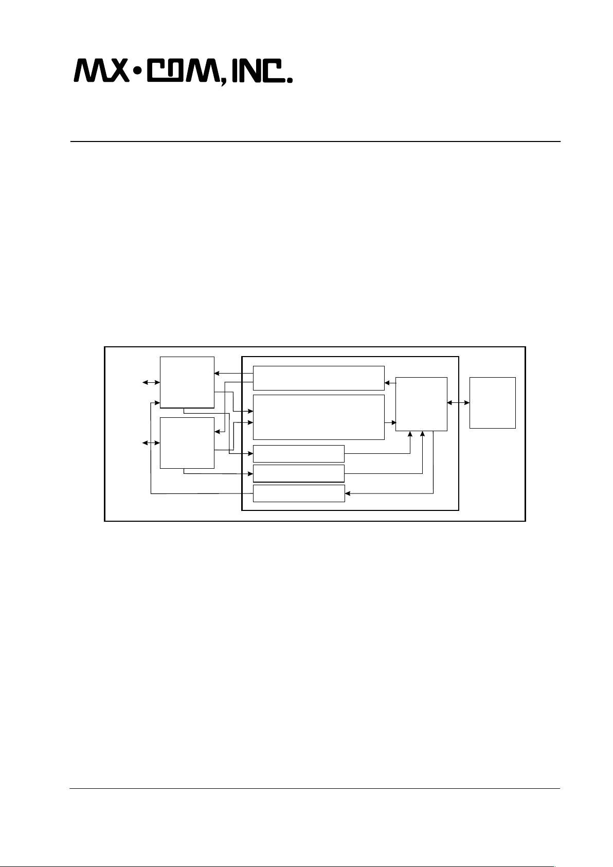
'C-BUS'
SERIAL
INTERFACE
PHONE
LINE
CMX860
PHONE
INTERFACE
LINE
INTERFACE
HOST
µC
TX USART / FSK MODULATOR
& TONE / DTMF GENERATOR
RX USART / FSK RECEIVER
CALL PROGRESS, CAS &
ANSWER TONE DETECTOR
DTMF DECODER
RING DETECTOR
HOOK DETECTOR
RELAY DRIVER
The CMX860 is a flexible, low power Telephone Signaling Transceiver IC designed for use in a wide range of
line-powered telephone equipment.
The IC combines the functions of a DTMF encoder and decoder, V.23 modulator and demodulator plus call
progression circuitry with analog switching between line and phone interfaces. Ring detection, local phone offhook detection, and a relay for line hook-switch operation are also provided under the control of C-BUS. The
ring and hook detectors operate while the remainder of the IC is powersaved, generating an interrupt to wakeup the host
µC when further processing or signaling is required.
All on-chip functions and switching arrangements are controlled via a serial bus (C-BUS). The CMX860 is
designed to operate at 2.7V and utilizes MX-COM’s low power DTMF decoder and V.23 modem technology.
The CMX860 is available in 28-pin SSOP (CMX860D6) and 28-pin SOIC (CMX860D1) packages.
Page 2

Telephone Signaling Transceiver 2 CMX860 Advance Information
¤¤¤¤2000 MX-COM, Inc. www.mxcom.com tel: 800 638 5577 336 744 5050 fax: 336 744 5054 Doc. # 20480222.001
4800 Bethania Station Road, Winston-Salem, NC 27105-1201 USA All trademarks and service marks are held by their respective companies.
CONTENTS
Section Page
1. Block Diagram............................................................................................................... 4
2. Signal List...................................................................................................................... 5
3. External Components ................................................................................................... 7
3.1 Ring Detector Interface.........................................................................................................9
3.2 Hook Detector Interface...................................................................................................... 10
3.3 Line Interface...................................................................................................................... 10
3.4 Phone Interface .................................................................................................................. 10
4. General Description .................................................................................................... 11
4.1 Tx USART ..........................................................................................................................11
4.2 FSK Modulator.................................................................................................................... 12
4.3 Tx Filter and Equalizer........................................................................................................ 12
4.4 DTMF/Tones Generator...................................................................................................... 12
4.5 Tx Level Control and Output Buffers ................................................................................... 12
4.6 DTMF Decoder and Tone Detectors ................................................................................... 12
4.7 Rx Modem Filter and Equalizer........................................................................................... 13
4.8 FSK Demodulator ............................................................................................................... 13
4.9 Rx Data Register and USART............................................................................................. 14
4.10 Rx Modem Pattern Detectors (and Descrambler)............................................................. 14
4.11 Analog Signal Routing ..................................................................................................... 15
4.12 C-BUS Interface............................................................................................................... 15
4.12.1 General Reset Command (no data) ($01) ............................................................................ 16
4.12.2 General Control Register: 16-bit write-only ($E0)................................................................. 17
4.12.3 Transmit Mode Register: 16-bit write-only ($E1) .................................................................. 18
4.12.4 Receive Mode Register: 16-bit write-only ($E2) ................................................................... 20
4.12.5 Tx Data Register: 8-bit write-only ($E3) ............................................................................... 21
4.12.6 Rx Data Register: 8-bit read-only ($E5) ............................................................................... 21
4.12.7 Analog Signal Path Register: 8-bit write-only ($EC)............................................................. 22
4.12.8 Status Register: 16-bit read-only ($E6) ................................................................................ 23
4.12.9 Programming Register
(includes generation & detection of CAS): 16-bit write-only ($E8) ....................................... 26
4.12.10 Other Registers..................................................................................................................... 28
Page 3

Telephone Signaling Transceiver 3 CMX860 Advance Information
¤¤¤¤2000 MX-COM, Inc. www.mxcom.com tel: 800 638 5577 336 744 5050 fax: 336 744 5054 Doc. # 20480222.001
4800 Bethania Station Road, Winston-Salem, NC 27105-1201 USA All trademarks and service marks are held by their respective companies.
5. Application Notes........................................................................................................ 29
6. Performance Specification......................................................................................... 30
6.1 Electrical Performance........................................................................................................ 30
6.1.1 Absolute Maximum Ratings .................................................................................................. 30
6.1.2 Operating Limits.................................................................................................................... 30
6.1.3 Operating Characteristics ..................................................................................................... 31
6.1.4 Timing ................................................................................................................................... 35
6.2 Packages............................................................................................................................ 35
MX-COM, Inc. reserves the right to change specifications at any time and without notice.
Page 4
Telephone Signaling Transceiver 4 CMX860 Advance Information
¤¤¤¤2000 MX-COM, Inc. www.mxcom.com tel: 800 638 5577 336 744 5050 fax: 336 744 5054 Doc. # 20480222.001
4800 Bethania Station Road, Winston-Salem, NC 27105-1201 USA All trademarks and service marks are held by their respective companies.
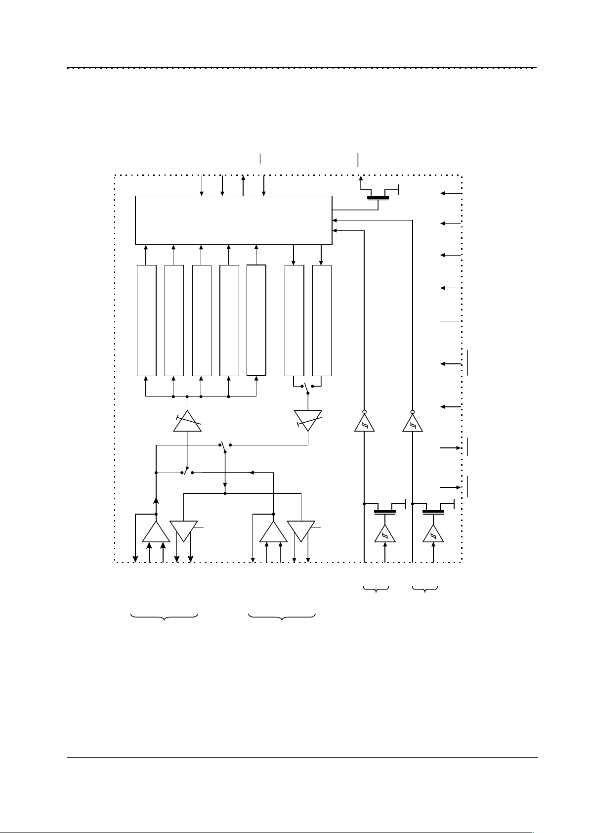
1. Block Diagram
CALL PROGRESS DECODER
DTMF DECODER
V.23 FSK DECODER
CAS DETECTOR
ANSWER TONE DETECTOR
DTMF/TONES GENERATOR
V.23 FSK GENERATOR
'C-BUS'
SERIAL
INTERFACE
SERIAL CLOCK
COMMAND DATA
REPLY DATA
CS
IRQ
V
BI AS
LINE
CONNECTION
PHONE
CONNECTION
RING
DETECT
OFF-HOOK
DETECT
XTAL
RDRV
XTAL/
CLOCK
RESET
DV
SS
AV
SS
DV
DD
AV
DD
EN
EN
LINE
RXAMPOUT
LINERX-
LINERX+
LINETX+
LINETX-
PHONE
RXAMPOUT
PHONERX-
PHONERX+
PHONETX+
PHONETX-
RT
RD
HT
HD
+
-
-
+
-
+
-
+
Figure 1: Block Diagram
Page 5
Telephone Signaling Transceiver 5 CMX860 Advance Information
¤¤¤¤2000 MX-COM, Inc. www.mxcom.com tel: 800 638 5577 336 744 5050 fax: 336 744 5054 Doc. # 20480222.001
4800 Bethania Station Road, Winston-Salem, NC 27105-1201 USA All trademarks and service marks are held by their respective companies.
2. Signal List
CMX860
D6, D1
Signal
Pin No. Name Type
Description
1
XTAL
output The output of the on-chip Xtal oscillator inverter.
2 XTAL/CLOCK input The input to the oscillator inverter from the Xtal circuit or
external clock source.
3
RDRV
output Relay drive output, low resistance pull down to DV
SS
when active and medium resistance pull up to DV
DD
when inactive.
4 DVSS Power The digital negative supply rail (ground).
5 RD input Schmitt trigger input to the Ring signal detector. Connect
to DV
SS
if Ring Detector not used.
6 RT bi-directional Open drain output and Schmitt trigger input forming part
of the Ring signal detector. Connect to DV
DD
if Ring
Detector not used.
7
RESET
input An active-low reset pin. Can be used as part of a power-
up reset function.
8 LINE
RXAMPOUT
output The output of the Phone Rx Input Amplifier.
9 LINERX- input The inverting input to the Phone Rx Input Amplifier.
10 LINERX+ input The non-inverting input to the Phone Rx Input Amplifier.
11 PHONE
RXAMPOUT
output The output of the Line Rx Input Amplifier.
12 PHONERX- input The inverting input to the Line Rx Input Amplifier.
13 PHONERX+ input The non-inverting input to the Line Rx Input Amplifier.
14 AVSS Power The analog negative supply rail (ground).
15 V
BIAS
output Internally generated bias voltage of approximately
AV
DD
/2, except when the device is in ‘Powersave’ mode
when V
BIAS
will discharge to AVSS. Should be decoupled
to AV
SS
by a capacitor mounted close to the device pins.
16 PHONETX- output The inverted output of the Phone Tx Output Buffer.
17 PHONETX+ output The non-inverted output of the Phone Tx Output Buffer.
18 LINETX- output The inverted output of the Line Tx Output Buffer.
19 LINETX+ output The non-inverted output of the Line Tx Output Buffer.
20 AVDD Power The analog positive supply rail. Levels and thresholds
within the device are proportional to this voltage.
21 HT bi-directional Open drain output and Schmitt trigger input forming part
of the Hook signal detector. Connect to DV
DD
if Hook
Detector not used.
22 HD input Schmitt trigger input to the Hook signal detector.
Connect to DV
SS
if Hook Detector not used.
23
CS
input
The C-BUS chip select input from the
µC.
24 COMMAND DATA input
The C-BUS serial data input from the
µC.
25 SERIAL CLOCK input
The C-BUS serial clock input from the
µC.
Page 6

Telephone Signaling Transceiver 6 CMX860 Advance Information
¤¤¤¤2000 MX-COM, Inc. www.mxcom.com tel: 800 638 5577 336 744 5050 fax: 336 744 5054 Doc. # 20480222.001
4800 Bethania Station Road, Winston-Salem, NC 27105-1201 USA All trademarks and service marks are held by their respective companies.
26 REPLY DATA tri-state
A 3-state C-BUS serial data output to the
µC. This output
is high impedance when not sending data to the
µC.
27
IRQ
output
A ‘wire-ORable’ output for connection to a
µC Interrupt
Request input. This output is pulled-down to DV
SS
when
active and is high impedance when inactive. An external
pull-up resistor is required i.e. R1 of Figure 2.
28 DVDD Power The digital positive supply rail. Levels and thresholds
within the device are proportional to this voltage.
The J5 package is only available as samples.
Table 1: Signal List
Page 7
Telephone Signaling Transceiver 7 CMX860 Advance Information
¤¤¤¤2000 MX-COM, Inc. www.mxcom.com tel: 800 638 5577 336 744 5050 fax: 336 744 5054 Doc. # 20480222.001
4800 Bethania Station Road, Winston-Salem, NC 27105-1201 USA All trademarks and service marks are held by their respective companies.
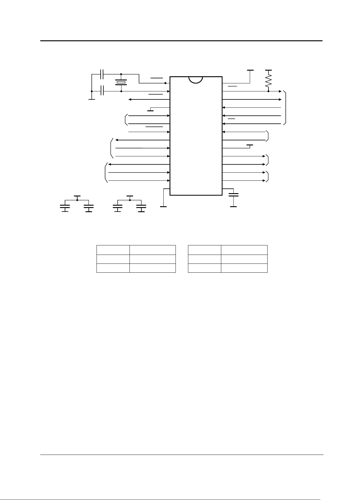
3. External Components
CMX860
D6/D1
1
C1
C2
C3
X1
XTAL
XTAL/CLOCK
'C-BUS'
to/from
µC
Ring
Detector
Hook
Detector
Phone
Interface
Line
Interface
Phone
Interface
Line
Interface
SERIAL CLOCK
COMMAND DATA
REPLY DATA
CS
HD
HT
IRQ
RDRV
RT
RESET
LINERXAMPOUT
LINERX+
LINERX-
PHONETX+
LINETX+
PHONERX-
PHONERXAMPOUT
PHONERX+
PHONETX-
LINETX-
RD
DV
DD
AV
SS
AV
SS
AV
SS
DV
SS
V
BI AS
2
5
6
8
9
10
11
7
12
13
14 15
16
17
18
19
20
21
22
23
24
25
26
27
28
R1
DV
DD
DV
DD
DV
SS
3
4
AV
DD
C6
C7
+
AV
DD
AV
SS
AV
SS
C4
C5
+
DV
DD
DV
SS
DV
SS
Figure 2: Recommended External Components for a Typical Application
R1
100k
Ω
C1, C2 22pF
X1 11.0592MHz C3, C4 100nF
or 12.288MHz C5 10uF
Resistors ±5%, capacitors ±20% unless otherwise stated.
Table 2: Recommended External Components for a Typical Application
This device is capable of detecting and decoding small amplitude signals. To achieve this DV
DD,
AV
DD,
and
V
BIAS
should be decoupled and the receive path protected from extraneous in-band signals. It is
recommended that the printed circuit board be laid out with both AV
SS
and DVSS ground planes in the
CMX860 area, as shown in Figure 3, with provision to make a link between them close to the CMX860. To
provide a low impedance connection to ground, the decoupling capacitors (C3-C7) must be mounted as close
to the CMX860 as possible and connected directly to their respective ground plane. This will be achieved
more easily by using surface mounted capacitors.
V
BIAS
is used as an internal reference for detecting and generating the various analog signals. It must be
carefully decoupled, to ensure its integrity. Apart from the decoupling capacitor shown (C3), no other loads
are allowed. If V
BIAS
needs to be used to set external analog levels, it must be buffered with a high input
impedance buffer. The DV
SS
connections to the Xtal oscillator capacitors C1 and C2 should also be of low
impedance and preferably be part of the DV
SS
ground plane to ensure reliable start up of the oscillator.
Page 8

Telephone Signaling Transceiver 8 CMX860 Advance Information
¤¤¤¤2000 MX-COM, Inc. www.mxcom.com tel: 800 638 5577 336 744 5050 fax: 336 744 5054 Doc. # 20480222.001
4800 Bethania Station Road, Winston-Salem, NC 27105-1201 USA All trademarks and service marks are held by their respective companies.
CMX860
1
2
3
4
5
6
7
8
9
10
11
12
13
14
15
16
17
18
19
20
21
22
23
24
25
26
27
28
AV
SS
AV
SS
V
BI AS
DV
SS
Provision
for a
Wire Link
DV
SS
DV
DD
C3
C7
L2
L1
C6
C5
C4
DV
DD
AV
DD
AV
DD
+
+
Figure 3: Recommended Power Supply Connections and De-coupling
ANALOG DIGITAL
C3, C6 100nF C4 100nF
C7
10
µF
C5
10µF
L2 100nH L1 100nH
Note: Inductors L1 and L2 can be omitted but this may degrade system performance.
Table 3: Recommended Power Supply Connections and De-coupling
Page 9
Telephone Signaling Transceiver 9 CMX860 Advance Information
¤¤¤¤2000 MX-COM, Inc. www.mxcom.com tel: 800 638 5577 336 744 5050 fax: 336 744 5054 Doc. # 20480222.001
4800 Bethania Station Road, Winston-Salem, NC 27105-1201 USA All trademarks and service marks are held by their respective companies.
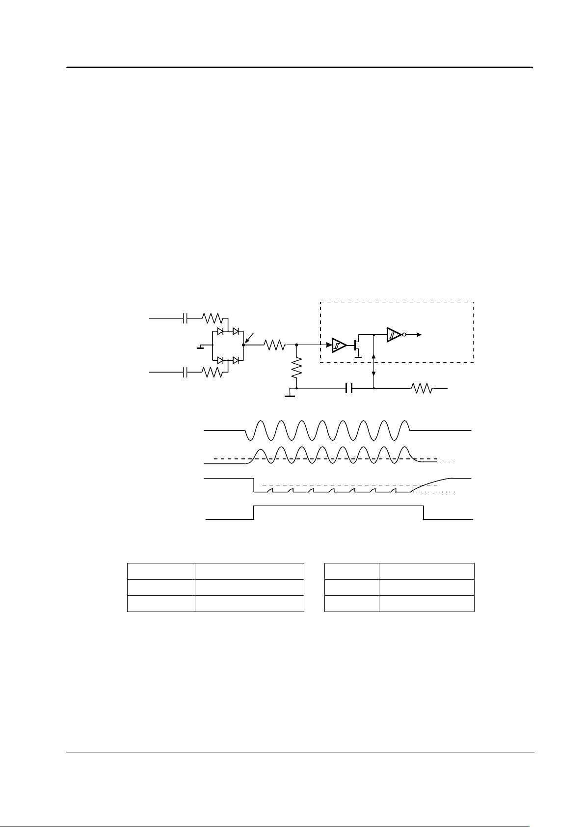
3.1 Ring Detector Interface
Figure 4 shows how the CMX860 may be used to detect the large amplitude ringing signal voltage present on
the 2-wire line at the start of an incoming telephone call.
The ring signal is usually applied at the subscriber's exchange as an ac voltage inserted in series with one of
the telephone wires and will pass through either C20 and R20 or C21 and R21 to appear at the top end of
R22 (point X in Figure 4) in a rectified and attenuated form.
The signal at point X is further attenuated by the potential divider formed by R22 and R23 before being
applied to the CMX860 RD input. If the amplitude of the signal appearing at RD is greater than the input
threshold (Vt
HI
) of Schmitt trigger 'A' then the N transistor connected to RT will be turned on, pulling the
voltage at RT to DV
SS
by discharging the external capacitor C22. The output of the Schmitt trigger 'B' will then
go high, setting bit 14 (Ring Detect) of the Status Register.
The minimum amplitude ringing signal that is certain to be detected is:
( 0.7 + Vt
HI
x [R20 + R22 + R23] / R23 ) x 0.707V
RMS
where Vt
HI
is the high-going threshold voltage of the Schmitt trigger A (see Section 6.1).
With R20-22 all 470k
Ω as Figure 4, then setting R23 to 68kΩ will guarantee detection of ringing signals of
40Vrms and above for DV
DD
over the range 3V to 5V.
2-Wire
Telephone
Line
RD
CMX860
To Status
Register
RT
DV
DD
DV
SS
DV
SS
D1 - 4
C20
C22
R20
R21
R22
R23
R24
C21
RT
Status Register bit 14
(Ring Detect)
Bridge rectifier output (X)
Ring signal
Vt
HI
DV
SS
DV
SS
Vt
HI
A
B
X
Figure 4: Ring Signal Detector Interface Circuit
R20, 21, 22
470k
Ω
C20, 21
0.1µF
R23 See text C22
0.33
µF
R24
470k
Ω
D1-4 1N4004
Resistors ±5%, capacitors ±20%, unless otherwise stated
If the time constant of R24 and C22 is large enough then the voltage on RT will remain below the threshold of
the 'B' Schmitt trigger for the duration of a ring cycle.
The time for the voltage on RT to charge from DV
SS
towards DVDD can be derived from the formula:
V
RT
= DV
DD
x [1 - exp(-t/(R24 x C22)) ]
As the Schmitt trigger high-going input threshold voltage (Vt
HI
) has a minimum value of 0.56 x DVDD, then the
Schmitt trigger B output will remain high for a time of at least 0.821 x R24 x C22 following a pulse at RD.
Page 10

Telephone Signaling Transceiver 10 CMX860 Advance Information
¤¤¤¤2000 MX-COM, Inc. www.mxcom.com tel: 800 638 5577 336 744 5050 fax: 336 744 5054 Doc. # 20480222.001
4800 Bethania Station Road, Winston-Salem, NC 27105-1201 USA All trademarks and service marks are held by their respective companies.
The values of R24 and C22 given in Figure 4 (470kΩ and 0.33µF) give a minimum RT charge time of 100ms,
which is adequate for ring frequencies of 10Hz or above.
Note, that the circuit will also respond to a telephone line voltage reversal. If necessary, the
µC can
distinguish between a Ring signal and a line voltage reversal by measuring the time that bit 14 of the Status
Register (Ring Detect) is high.
If the Ring detect function is not used then pin RD should be connected to DV
SS
and RT to DV
DD
.
3.2 Hook Detector Interface
This is identical internally to the Ring Detector interface circuit and similar components could be used
externally, with appropriate values, if hook detection is to be performed by detecting a voltage change across
the tip and ring lines to the local phone.
3.3 Line Interface
Figure 5: 2-Wire Line Interface Circuit: Application Circuits are TBD
3.4 Phone Interface
Figure 6: 2-Wire Phone Interface Circuit: Application Circuits are TBD
Page 11
Telephone Signaling Transceiver 11 CMX860 Advance Information
¤¤¤¤2000 MX-COM, Inc. www.mxcom.com tel: 800 638 5577 336 744 5050 fax: 336 744 5054 Doc. # 20480222.001
4800 Bethania Station Road, Winston-Salem, NC 27105-1201 USA All trademarks and service marks are held by their respective companies.
4. General Description
The CMX860 transmit and receive operating modes are independently programmable.
The transmit mode can be set to any one of the following:
• V.23 modem. 1200 or 75bps FSK.
• DTMF transmit.
• Single tone transmit (from a range of modem calling, answer and other tone frequencies)
• User programmed tone or tone pair transmit (programmable frequencies and levels)
• Disabled.
The receive mode can be set to any one of the following:
• V.23 modem. 1200 or 75bps FSK.
• DTMF decode.
• 2100Hz and 2225Hz answer tone detect.
• Call progress signal detect.
• User programmed tone or tone pair detect.
• Disabled.
The CMX860 may also be set into a Powersave mode that disables all circuitry except for the C-BUS
interface, the Ring Detector and the Hook Detector.
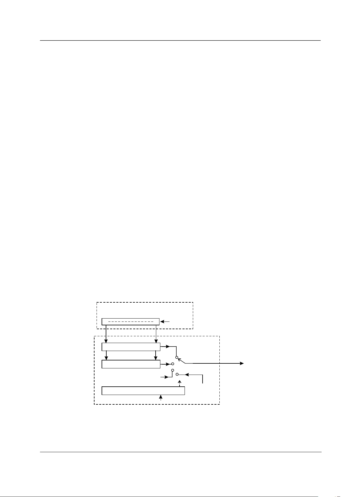
4.1 Tx USART
A flexible Tx USART is provided. It can be programmed to transmit continuous patterns, Start-Stop characters
or Synchronous Data.
In both Synchronous Data and Start-stop modes the data to be transmitted is written by the µC into the 8-bit
C-BUS Tx Data Register from which it is transferred to the Tx Data Buffer.
If Synchronous Data mode has been selected the 8 data bits in the Tx Data Buffer are transmitted serially, b0
being sent first.
In Start-stop mode a single Start bit is transmitted, followed by 5, 6, 7 or 8 data bits from the Tx Data Buffer b0 first - followed by an optional Parity bit then - normally - one or two Stop bits. The Start, Parity and Stop
bits are generated by the USART as determined by the Tx Mode Register settings and are not taken from the
Tx Data Register.
Tx Data Register
'C-BUS' Interface
Tx USART
Modem bit rate clock
Continuous
patterns
To FSK
Modulator
Tx data
from µC
Start/Stop
bits
Tx Data Buffer
Parity bit generator
USART Control
7 0
Figure 7: Tx USART
Page 12

Telephone Signaling Transceiver 12 CMX860 Advance Information
¤¤¤¤2000 MX-COM, Inc. www.mxcom.com tel: 800 638 5577 336 744 5050 fax: 336 744 5054 Doc. # 20480222.001
4800 Bethania Station Road, Winston-Salem, NC 27105-1201 USA All trademarks and service marks are held by their respective companies.
Every time the contents of the C-BUS Tx Data Register are transferred to the Tx Data Buffer the Tx Data
Ready flag bit of the Status Register is set to 1 to indicate that a new value should be loaded into the C-BUS
Tx Data Register. This flag bit is cleared to 0 when a new value is loaded into the Tx Data Register.
StartTx Line Signal:
Tx Data Ready flag bit:
Par'y StopB0 B1 B7
Figure 8: Tx USART Function (Start-Stop mode, 8 Data Bits + Parity)
If a new value is not loaded into the Tx Data Register in time for the next Tx Data Register to Tx Data Buffer
transfer then the Status Register Tx Data Underflow bit will be set to 1. In this event the contents of the Tx
Data Buffer will be re-transmitted if Synchronous Data mode has been selected, or if the Tx modem is in
Start-stop mode then a continuous Stop signal (1) will be transmitted until a new value is loaded into the Tx
Data Register.
The transmitted bit rates are determined by the XTAL frequency.
4.2 FSK Modulator
Serial data from the USART is fed to the FSK modulator. One of two frequencies is generated according to
the current transmit data bit.
4.3 Tx Filter and Equalizer
The FSK modulator output signal is fed through the Transmit Filter and Equalizer block that limits the out-ofband signal energy to acceptable limits. When transmitting 1200bps FSK, this block includes a fixed
compromise line equalizer that may be enabled or disabled by bit 10 of the General Control Register. The
amount of Tx equalization provided compensates for one quarter of the relative amplitude and delay distortion
of ETS Test Line 1 over the frequency band used.
4.4 DTMF/Tones Generator
In DTMF/Tones mode, this block generates DTMF signals or single or dual frequency tones.
4.5 Tx Level Control and Output Buffers
The outputs (if present) of the Transmit Filter and DTMF/Tone Generator are selected then passed through
the programmable Tx Level Control and via a switched data path to the Line and Phone Output Buffers.
These Tx Output Buffers have symmetrical outputs to provide sufficient line voltage swing at low values of
AV
DD
and to reduce harmonic distortion of the signal. The Line and Phone Output Buffers can be separately
enabled by setting bits 2 and 1 respectively of the Analog Signal Path Register.
4.6 DTMF Decoder and Tone Detectors
In Rx Tones Detect mode the received signal, after passing through the Rx Gain Control block, is fed to the
DTMF decoder and CAS Tones/Call Progress/Answer Tone detector. The user may select one of four
separate operations:
The DTMF decoder detects standard DTMF signals. A valid DTMF signal will set bit 5 of the Status Register
to 1 for as long as the signal is detected. The DTMF signal is then decoded and output in bits 0 to 3 of the
Status Register.
The programmable tone pair detector includes two separate tone detectors (see Figure 16). The first detector
will set bit 6 of the Status Register for as long as a valid signal is detected, the second detector sets bit 7, and
bit 10 of the Status Register will be set when both tones are detected. The frequency and bandwidth of each
detector can be set in the Programming Register. Without programming, the default values in the
Programming Register are set for CAS tone detection.
The Call Progress detector measures the amplitude of the signal at the output of a 275 Hz - 665 Hz bandpass
filter and sets bit 10 of the Status Register to 1 when the signal level exceeds the measurement threshold.
Page 13

Telephone Signaling Transceiver 13 CMX860 Advance Information
¤¤¤¤2000 MX-COM, Inc. www.mxcom.com tel: 800 638 5577 336 744 5050 fax: 336 744 5054 Doc. # 20480222.001
4800 Bethania Station Road, Winston-Salem, NC 27105-1201 USA All trademarks and service marks are held by their respective companies.
-60
-50
-40
-30
-20
-10
0
10
00.511.522.533.54
kHz
dB
Figure 9: Response of the Call Progress Filter
The Answer Tone detector measures both amplitude and frequency of the received signal and sets bit 6 or bit
7 respectively of the Status Register when a valid 2225Hz or 2100Hz signal is received.
4.7 Rx Modem Filter and Equalizer
When the receive part of the CMX860 is operating as a modem, the received signal is fed to a bandpass filter
to attenuate unwanted signals and to provide fixed compromise line equalization. The line equalizer may be
enabled or disabled by bit 10 of the General Control Register and compensates for one quarter of the relative
amplitude and delay distortion of ETS Test Line 1.
A typical response of this filter, including the line equalizer is shown in Figure 10. The effect of external
components (see Figure 5 and Figure 6) should also be considered in determining the overall response.
-60
-50
-40
-30
-20
-10
0
10
00.511.522.533.54
kHz
dB
Figure 10: V.23 Rx Filters
The signal level at the output of the Receive Modem Filter and Equalizer is measured in the Modem Energy
Detector block, compared to a threshold value, and the result controls bit 10 of the Status Register.
The output of the Receive Modem Filter and Equalizer is also fed to the FSK demodulator.
4.8 FSK Demodulator
The FSK demodulator recognizes individual frequencies as representing received ‘1’ or ‘0’ data bits:
The FSK demodulator produces a serial data bit stream which is fed to the Rx USART block, see
Figure 11. This bit stream is also monitored for continuous ‘1010’s and for continuous 1’s. The outputs of
these pattern detectors control bits 9 and 7 respectively of the Status Register.
Page 14

Telephone Signaling Transceiver 14 CMX860 Advance Information
¤¤¤¤2000 MX-COM, Inc. www.mxcom.com tel: 800 638 5577 336 744 5050 fax: 336 744 5054 Doc. # 20480222.001
4800 Bethania Station Road, Winston-Salem, NC 27105-1201 USA All trademarks and service marks are held by their respective companies.
4.9 Rx Data Register and USART
The Rx USART can be programmed to treat the received data bit stream as Synchronous data or as StartStop characters.
In Synchronous mode the received data bits are all fed into the Rx Data Buffer which is copied into the C-BUS
Rx Data Register after every 8 bits.
In Start-stop mode the USART Control logic looks for the start of each character, then feeds only the required
number of data bits (not parity) into the Rx Data Buffer. The parity bit (if used) and the presence of a Stop bit
are then checked and the data bits in the Rx Data Buffer copied to the C-BUS Rx Data Register.
Bit rate clock
Start/Stop bits
Rx Data Buffer
Parity bit checker
USART Control
Rx Data Register
'C-BUS' Interface
Rx USART
Rx data
to µC
7 0
From FSK
Demodulator
b9
Status Register:
b7
"1010"
Detector
Continuous
1s Detector
Figure 11: Rx Modem Data Paths
Whenever a new character is copied into the C-BUS Rx Data Register, the Rx Data Ready flag bit of the
Status Register is set to 1 to prompt the µC to read the new data, and, in Start-stop mode, the Even Rx Parity
flag bit of the Status Register is updated.
In Start-stop mode, if the Stop bit is missing (received as a ‘0’ instead of a ‘1’) the received character will still
be placed into the Rx Data Register and the Rx Data Ready flag bit set, but the Status Register Rx Framing
Error bit will also be set to ‘1’ and the USART will re-synchronize onto the next ‘1’ – ‘0’ (Stop – Start)
transition. The Rx Framing Error bit will remain set until the next character has been received.
Start
Rx Signal:
Rx Data Ready flag bit:
Par'y
Stop
B0
B1 B7
Figure 12: Rx USART Function (Start-stop mode, 8 Data Bits + Parity)
If the µC has not read the previous data from the Rx Data Register by the time that new data is copied to it
from the Rx Data Buffer then the Rx Data Overflow flag bit of the Status Register will be set to 1.
The Rx Data Ready flag and Rx Data Overflow bits are cleared to 0 when the Rx Data Register is read by the
µC.
4.10 Rx Modem Pattern Detectors (and Descrambler)
The '1010' pattern detector will set bit 9 of the Status Register when 32 bits of alternating 1's and 0's have
been received. The continuous 1's detector will set bit 7 of the Status Register when 32 consecutive 1's have
been received. Both pattern detectors will hold their 'detect' output for 12 bit times after the end of the
detected pattern unless the received bit rate or operating mode is changed, in which case the detectors are
reset within 2ms.
Page 15

Telephone Signaling Transceiver 15 CMX860 Advance Information
¤¤¤¤2000 MX-COM, Inc. www.mxcom.com tel: 800 638 5577 336 744 5050 fax: 336 744 5054 Doc. # 20480222.001
4800 Bethania Station Road, Winston-Salem, NC 27105-1201 USA All trademarks and service marks are held by their respective companies.
4.11 Analog Signal Routing
The routing of signals to and from the Line and Phone interfaces is performed by bits 0 to 3 of the Analog
Signal Path Register. Please note that bits 4 to 7 of this register are reserved for future use and should be set
to zero for the moment.
4.12 C-BUS Interface
This block provides for the transfer of data and control or status information between the CMX860’s internal
registers and the µC over the C-BUS serial bus. Each transaction consists of a single Register Address byte
sent from the µC which may be followed by one or more data byte(s) sent from the µC to be written into one
of the CMX860’s Write Only Registers, or one or more byte(s) of data read out from one of the CMX860’s
Read Only Registers, as illustrated in Figure 13.
Data sent from the µC on the Command Data line is clocked into the CMX860 on the rising edge of the Serial
Clock input. Reply Data sent from the CMX860 to the µC is valid when the Serial Clock is high. The
CS line
must be held low during a data transfer and kept high between transfers. The C-BUS interface is compatible
with most common µC serial interfaces and may be easily implemented with general-purpose µC I/O pins
controlled by a simple software routine. Figure 21 provides detailed C-BUS timing requirements.
The following C-BUS addresses and registers are used by the CMX860:
Register Read/Write Address
General Reset Command (address only, no data). $01
General Control Register 16-bit write only $E0
Transmit Mode Register 16-bit write-only $E1
Receive Mode Register 16-bit write-only $E2
Transmit Data Register 8-bit write only $E3
Receive Data Register 8-bit read-only $E5
Status Register 16-bit read-only $E6
Programming Register 16-bit write-only $E8
Analog Signal Path Register 8-bit write-only $EC
Notes:
1. The C-BUS addresses $E9, $EA and $EB are allocated for production testing and should not be
accessed in normal operation.
2. The C-BUS address $E4 is allocated for internal use and should not be accessed in normal operation.
3. In several registers, there are bit patterns whose function is not specified. These modes should not be
accessed in normal operation and no guarantee is given that any use of these bits will be supported in the
future.
Page 16

Telephone Signaling Transceiver 16 CMX860 Advance Information
¤¤¤¤2000 MX-COM, Inc. www.mxcom.com tel: 800 638 5577 336 744 5050 fax: 336 744 5054 Doc. # 20480222.001
4800 Bethania Station Road, Winston-Salem, NC 27105-1201 USA All trademarks and service marks are held by their respective companies.
4.12.1 General Reset Command (no data) ($01)
This command resets the device and clears all bits of the General Control, Transmit Mode and Receive Mode
Registers and bits 15 and 13-0 of the Status Register.
Whenever power is applied to the CMX860 a General Reset command should be sent to the device, after
which the General Control Register should be set as required.
CS
a) Single byte from µC
SERIAL CLOCK
COMMAND DATA
Address (01 Hex = Reset)
= Level not important
Note:
The SERIAL CLOCK line may be high
or low at the start and end of each
transaction.
Hi-Z
REPLY DATA
7
654
321
0
b) One Address and one Data byte from µC
CS
SERIAL CLOCK
COMMAND DATA
Address
Hi-Z
Data to CMX860
REPLY DATA
7
654
321
0
7
654
321
0
c) One Address and 2 Data bytes from µC
CS
SERIAL CLOCK
COMMAND DATA
Address
Hi-Z
First (msb) data
byte to CMX860
Second (lsb) data
byte to CMX860
REPLY DATA
7
654
321
0
7
654
321
0
7
654
321
0
d) One Address byte from µC and one Reply byte from CMX860
CS
SERIAL CLOCK
Hi-Z
Address
Data from CMX860
COMMAND DATA
REPLY DATA
7
654
321
0
7
654
321
0
7
654
321
0
e) One Address byte from µC and 2 Reply bytes from CMX860
CS
SERIAL CLOCK
Hi-Z
Address
First (msb) byte
from CMX860
Second(lsb) byte
from CMX860
COMMAND DATA
REPLY DATA
7
654
321
0
7
654
321
0
Figure 13: C-BUS Transactions
Page 17

Telephone Signaling Transceiver 17 CMX860 Advance Information
¤¤¤¤2000 MX-COM, Inc. www.mxcom.com tel: 800 638 5577 336 744 5050 fax: 336 744 5054 Doc. # 20480222.001
4800 Bethania Station Road, Winston-Salem, NC 27105-1201 USA All trademarks and service marks are held by their respective companies.
4.12.2 General Control Register: 16-bit write-only ($E0)
This register controls general features of the CMX860 such as the Powersave mode, the IRQ mask bits and the
Relay Drive output. It also allows the fixed compromise equalizers in the Tx and Rx signal paths to be disabled if
desired, and sets the internal clock dividers to use either a 11.0592 or a 12.288 MHz XTAL frequency. All bits of
this register are cleared to 0 by a General Reset command.
Bit:
15 14 13 12 11 10 9 8 7 6 5 4 3 2 1 0
0 0 0 Xtal freq
Hook
IRQ Mask
Equ Rlydrv Pwr Rst Irqnen IRQ Mask Bits
Reserved
Bit 15-13
Reserved, set to 000
Xtal Frequency
Bit 12
This bit should be set according to the Xtal frequency.
b12 = 1 11.0592MHz
b12 = 0 12.2880MHz
Hook Detect IRQ
Mask
Bit 11
This bit affects the operation of the IRQ bit of the Status Register as described in section 4.12.8
Tx and Rx Fixed
Compromise
Equalizer
Bit 10
This bit allows the Tx and Rx fixed compromise equalizer in the modem transmit and receive
filter blocks to be disabled
b10 = 1 Disable equalizer
b10 = 0 Enable equalizer (1200bps modem mode)
Relay Drive
Bit 9
This bit directly controls the
RDRV output pin.
b9 = 1
RDRV output pin pulled to DV
SS
b9 = 0
RDRV output pin pulled to DV
DD
Power-up
Bit 8
This bit controls the internal power supply to most of the internal circuits, including the Xtal
oscillator and V
BIAS
supply. Note that the General Reset command clears this bit, putting the
device into Powersave mode.
When the device is switched from Powersave mode to normal operation by setting the Power-
up bit to 1, about 20ms should be allowed for the external circuits, Xtal oscillator, and V
BIAS
to
stabilize before starting to use the transmitter or receiver.
Changing the Power-up bit to 1 clears all bits of the Transmit Mode and Receive Mode
Registers and clears b15 and b13-0 of the Status Register.
b8 = 1 Device powered up normally
b8 = 0
Powersave mode (all circuits except Ring Detect, Hook Detect,
RDRV and
C-BUS interface disabled)
Reset
Bit 7
Setting this bit to 1 resets the CMX860’s internal circuitry, clearing all bits of the Transmit and
Receive Mode Registers and b15 and b13-0 of the Status Register.
b7 = 1 Internal circuitry in a reset condition.
b7 = 0 Normal operation
EN IRQ
(
IRQ Output
Enable)
Bit 6
Setting this bit to 1 enables the
IRQ output pin.
b6 = 1
IRQ pin driven low (to DV
SS
) if the IRQ bit of the Status Register = 1
b6 = 0
IRQ pin disabled (high impedance)
IRQ Mask Bits
Bit 5-0
These bits affect the operation of the IRQ bit of the Status Register as described in
Section 4.12.8.
Table 4: General Control Register
Page 18

Telephone Signaling Transceiver 18 CMX860 Advance Information
¤¤¤¤2000 MX-COM, Inc. www.mxcom.com tel: 800 638 5577 336 744 5050 fax: 336 744 5054 Doc. # 20480222.001
4800 Bethania Station Road, Winston-Salem, NC 27105-1201 USA All trademarks and service marks are held by their respective companies.
4.12.3 Transmit Mode Register: 16-bit write-only ($E1)
This register controls the CMX860 transmit signal type and level. All bits of this register are cleared to 0 by a
General Reset command, in Powersave mode, or when b7 (Reset) of the General Control Register is 1.
Bit:
15 14 13 12 11 10 9 8 7 6 5 4 3 2 1 0
Tx mode = modem Tx level set to 00 set to 00
Start-stop /
synch data
# data bits /
synch data source
Tx mode = DTMF/Tones Tx level Unused, set to 0000 DTMF or Tone select
Tx mode = Disabled Set to 0000 0000 0000
Tx Mode
Bit 15-12
These 4 bits select the transmit operating mode.
b15 b14 b13 b12
0 1 0 1 V.23 FSK 1200bps
0 1 0 0 V.23 FSK 75bps
0 0 0 1 DTMF / Tones
0 0 0 0 Transmitter disabled
Tx Level
Bit 11-9
These 3 bits set the gain of the Tx Level Control block.
b11 b10 b9
1 1 1 0dB
1 1 0 -1.5dB
1 0 1 -3.0dB
1 0 0 -4.5dB
0 1 1 -6.0dB
0 1 0 -7.5dB
0 0 1 -9.0dB
0 0 0 -10.5dB
RESERVED
Bit 8-5
Reserved, set to 0000
Tx Data Format
(both FSK
modes)
Bit 4-3
These two bits select Synchronous or Start-stop mode and the addition of a parity bit to
transmitted characters in Start-stop mode.
b4 b3
1 1 Synchronous mode
1 0 Start-stop mode, no parity
0 1 Start-stop mode, even parity bit added to data bits
0 0 Start-stop mode, odd parity bit added to data bits
Tx Data and
Stop Bits
(FSK Start-stop
mode)
Bit 2-0
In Start-stop mode these three bits select the number of Tx data and stop bits
b2 b1 b0
1 1 1 8 data bits, 2 stop bits
1 1 0 8 data bits, 1 stop bit
1 0 1 7 data bits, 2 stop bits
1 0 0 7 data bits, 1 stop bit
0 1 1 6 data bits, 2 stop bits
0 1 0 6 data bits, 1 stop bit
0 0 1 5 data bits, 2 stop bits
0 0 0 5 data bits, 1 stop bit
Page 19

Telephone Signaling Transceiver 19 CMX860 Advance Information
¤¤¤¤2000 MX-COM, Inc. www.mxcom.com tel: 800 638 5577 336 744 5050 fax: 336 744 5054 Doc. # 20480222.001
4800 Bethania Station Road, Winston-Salem, NC 27105-1201 USA All trademarks and service marks are held by their respective companies.
Tx Data Source
(FSK
Synchronous
mode)
Bit 2-0
In Synchronous mode, (b4-3 = 11) these three bits select the source of the data fed to the Tx
FSK modulator.
b2 b1 b0
1 x x Data bytes from Tx Data Buffer
0 1 1 Continuous 1s
0 1 0 Continuous 0s
0 0 x Continuous alternating 1s and 0s
DTMF/Tones
Mode
Bit 8-0
If DTMF/Tones transmit mode has been selected (Tx Mode Register b15-12 = 0001) then b8-5
should be set to 0000 and b4-0 will select a DTMF signal or a fixed tone or one of four
programmed tones or tone pairs for transmission.
b4 = 0: Tx fixed tone or programmed tone pair
b3 b2 b1 b0 Tone frequency (Hz)
0 0 0 0 No tone
0 0 0 1 697
0 0 1 0 770
0 0 1 1 852
0 1 0 0 941
0 1 0 1 1209
0 1 1 0 1336
0 1 1 1 1477
1 0 0 0 1633
1 0 0 1 1300 (Calling tone)
1 0 1 0 2100 (Answer tone)
1 0 1 1 2225 (Answer tone)
1 1 0 0 Tone pair TA Programmed Tx tone / tone pair, see 4.12.9
1 1 0 1 Tone pair TB “
1 1 1 0 Tone pair TC “
1 1 1 1 CAS Tones by default Tx tone / tone pair TD when TD programmed
Tx DTMF
Bit 4 = 1
b3 b2 b1 b0 Low frequency (Hz) High frequency (Hz) Keypad symbol
0 0 0 0 941 1633 D
0 0 0 1 697 1209 1
0 0 1 0 697 1336 2
0 0 1 1 697 1477 3
0 1 0 0 770 1209 4
0 1 0 1 770 1336 5
0 1 1 0 770 1477 6
0 1 1 1 852 1209 7
1 0 0 0 852 1336 8
1 0 0 1 852 1477 9
1 0 1 0 941 1336 0
1 0 1 1 941 1209 *
1 1 0 0 941 1477 #
1 1 0 1 697 1633 A
1 1 1 0 770 1633 B
1 1 1 1 852 1633 C
Table 5: Transmit Mode Register
Page 20

Telephone Signaling Transceiver 20 CMX860 Advance Information
¤¤¤¤2000 MX-COM, Inc. www.mxcom.com tel: 800 638 5577 336 744 5050 fax: 336 744 5054 Doc. # 20480222.001
4800 Bethania Station Road, Winston-Salem, NC 27105-1201 USA All trademarks and service marks are held by their respective companies.
4.12.4 Receive Mode Register: 16-bit write-only ($E2)
This register controls the CMX860 receive signal type and level.
All bits of this register are cleared to 0 by a General Reset command, in Powersave mode or when b7 (Reset)
of the General Control Register is 1.
Bit:
15 14 13 12 11 10 9 8 7 6 5 4 3 2 1 0
Rx mode = modem Rx level Eq Set to 00 Start-stop/Synch
No. of bits and
parity
Rx mode = Tones detect Rx level DTMF/Tones/Call Progress select
Rx mode = Disabled Set to 0000 0000 0000
Rx Mode
Bit 15-12
These 4 bits select the receive operating mode.
b15 b14 b13 b12
0 1 0 1 V.23 FSK 1200bps
0 1 0 0 V.23 FSK 75bps
0 0 0 1 DTMF, Programmed tone pair, Answer Tone, Call Progress
detect
0 0 0 0 Receiver disabled
Rx Level
Bit 11-9
These three bits set the gain of the Rx Gain Control block.
b11 b10 b9
1 1 1 0dB
1 1 0 -1.5dB
1 0 1 -3.0dB
1 0 0 -4.5dB
0 1 1 -6.0dB
0 1 0 -7.5dB
0 0 1 -9.0dB
0 0 0 -10.5dB
Reserved
Bit 8-6
Reserved, set to 000
Rx USART
Setting (both
FSK modes)
Bit 5-3
These three bits select the Rx USART operating mode.
b5 b4 b3
1 1 1 Rx Synchronous mode
1 1 0 Rx Start-stop mode
0 x x Rx USART function disabled
Rx Data Bits and
parity (FSK
Start-stop mode)
Bit 2-0
In Start-stop mode these three bits select the number of data bits (plus any parity bit) in each
received character.
b2 b1 b0
1 1 1 8 data bits + parity
1 1 0 8 data bits
1 0 1 7 data bits + parity
1 0 0 7 data bits
0 1 1 6 data bits + parity
0 1 0 6 data bits
0 0 1 5 data bits + parity
0 0 0 5 data bits
Page 21

Telephone Signaling Transceiver 21 CMX860 Advance Information
¤¤¤¤2000 MX-COM, Inc. www.mxcom.com tel: 800 638 5577 336 744 5050 fax: 336 744 5054 Doc. # 20480222.001
4800 Bethania Station Road, Winston-Salem, NC 27105-1201 USA All trademarks and service marks are held by their respective companies.
Rx Data bits and
parity (FSK
Synchronous
mode)
Bit 2-0
These bits are ignored in Synchronous mode.
Tones Detect
mode
Bit 2-0
In Tones Detect Mode (Rx Mode Register b15-12 = 0001) b8-3 should be set to 000000.
Bits 2-0 select the detector type.
b2 b1 b0
1 0 0 Programmable Tone Pair Detect
0 1 1 Call Progress Detect
0 1 0 2100, 2225Hz Answer Tone Detect
0 0 1 DTMF Decode
0 0 0 Disabled
Table 6: Receive Mode Register
4.12.5 Tx Data Register: 8-bit write-only ($E3)
Bit:
7 6 5 4 3 2 1 0
Data bits to be transmitted
In Synchronous Tx data mode this register contains the next 8 data bits to be transmitted. Bit 0 is transmitted
first.
In Tx Start-stop mode the specified number of data bits will be transmitted from this register (b0 first). A Start
bit, a Parity bit (if required) and Stop bit(s) will be added automatically.
This register should only be written to when the Tx Data Ready bit of the Status Register is 1.
4.12.6 Rx Data Register: 8-bit read-only ($E5)
Bit:
7 6 5 4 3 2 1 0
Received data bits
In unformatted Rx data mode this register contains 8 received data bits, b0 of the register holding the earliest
received bit, b7 the latest.
In Rx Start-stop data mode this register contains the specified number of data bits from a received character,
b0 holding the first received bit.
Page 22

Telephone Signaling Transceiver 22 CMX860 Advance Information
¤¤¤¤2000 MX-COM, Inc. www.mxcom.com tel: 800 638 5577 336 744 5050 fax: 336 744 5054 Doc. # 20480222.001
4800 Bethania Station Road, Winston-Salem, NC 27105-1201 USA All trademarks and service marks are held by their respective companies.
4.12.7 Analog Signal Path Register: 8-bit write-only ($EC)
Bit:
7 6 5 4 3 2 1 0
0 0 0 0 Line to Drivers
Control
Line Driver
Enable
Phone Driver
Enable
Input Selector
Control
Reserved
Bit 7-4
Reserved, set to 0000
Line to Drivers
Control
Bit 3
This bit controls the switching of the signal path into the output drivers.
b3 = 1 Output drivers take their signal from the output of the Line input op-amp
b3 = 0 Output drivers take their signal from the on-chip DTMF/TONES/FSK Generator
Line Driver
Enable
Bit 2
This bit enables or disables the complementary Line Driver.
b2 = 1 Line Driver enabled
b2 = 0 Line Driver disabled & high impedance
Phone Driver
Enable
Bit 1
This bit enables or disables the complementary Phone Driver.
b1 = 1 Phone Driver enabled
b1 = 0 Phone Driver disabled & high impedance
Input Selector
Control
Bit 0
This bit selects between the Line and Phone as inputs to the CMX860’s decoders/detectors.
b0 = 1 Output of Line input op-amp to decoders/detectors
B0 = 0 Output of Phone input op-amp to decoders/detectors
Note:
Both op-amps remain powered up even when not selected (unless device is powersaved).
Table 7: Analog Signal Path Register
Page 23

Telephone Signaling Transceiver 23 CMX860 Advance Information
¤¤¤¤2000 MX-COM, Inc. www.mxcom.com tel: 800 638 5577 336 744 5050 fax: 336 744 5054 Doc. # 20480222.001
4800 Bethania Station Road, Winston-Salem, NC 27105-1201 USA All trademarks and service marks are held by their respective companies.
4.12.8 Status Register: 16-bit read-only ($E6)
Bits 15 and 13-0 of this register are cleared to 0 by a General Reset command, in Powersave mode, or when
b7 (Reset) of the General Control Register is 1.
Bit:
15 14 13 12 11 10 9 8 7 6 5 4 3 2 1 0
IRQ RD PF See below for uses of these bits
The meanings of the Status Register bits 12-0 depend on whether the receive circuitry is in Modem or Tones
Detect mode.
Status Register bits:
Rx Modem modes Rx Tones Detect modes ** IRQ Mask bit
b15 IRQ
b14 Set to 1 on Ring Detect b5
b13 Programming Flag bit. See 1.5.12.9 b4
b12
Set to 1 on Tx data ready.
Cleared by write to Tx Data Register
b3
b11
Set to 1 on Tx data underflow.
Cleared by write to Tx Data Register
b3
b10
1 when energy is detected in Rx
modem signal band
1 when energy is detected in Call
Progress band or when both
programmable tones are detected
b2
b9
1 when ‘1010..’ pattern is detected
in FSK modes
0
b1
b8 Set to 1 on Hook Detect B11
b7
1 when continuous 1’s pattern
detected in FSK modes
1 when 2100Hz answer tone or the
second programmable tone is
detected
b1
b6
Set to 1 on Rx data ready.
Cleared by read from Rx Data
Register
1 when 2225Hz answer tone or the
first programmable tone is detected
b0
b5
Set to 1 on Rx data overflow.
Cleared by read from Rx Data
Register
1 when DTMF code is detected
b0
b4 Set to 1 on Rx framing error 0 b3 Set to 1 on even Rx parity Rx DTMF code b3, see table b2 0 Rx DTMF code b2 b1 0 Rx DTMF code b1 b0 FSK frequency demodulator output Rx DTMF code b0 -
Table 8: Status Register
Notes: ** This column shows the corresponding IRQ Mask bits in the General Control Register. A 0 to 1
transition on any of the Status Register bits 14-5 will cause the IRQ bit b15 to be set to 1 if the corresponding
IRQ Mask bit is 1. The IRQ bit is cleared by a read of the Status Register or a General Reset command or by
setting b7 or b8 of the General Control Register to 1. The operation of the data demodulator and pattern
detector circuits within the CMX860 does not depend on the state of the Rx energy detect function.
Page 24

Telephone Signaling Transceiver 24 CMX860 Advance Information
¤¤¤¤2000 MX-COM, Inc. www.mxcom.com tel: 800 638 5577 336 744 5050 fax: 336 744 5054 Doc. # 20480222.001
4800 Bethania Station Road, Winston-Salem, NC 27105-1201 USA All trademarks and service marks are held by their respective companies.
Rx signal
Status Register bit 5,6,7,8,9 or 10
Status Register bit 15 (IRQ)
IRQ output
Notes:
Detect time
Note 1
Note 3
Note 2
1. IRQ will go high only if appropriate IRQ Mask bit in General Control Register is set.
The IRQ bit is cleared by a read of the Status Register.
2. output will go low when IRQ bit high if EN bit of General Control Register is setIRQ IRQ
3. In Rx Modem modes Status Register bits 5 and 6 are set by a Rx Data Ready or
Rx Data Underflow event and cleared by a read of the Rx Data Register
Hold time
Figure 14: Operation of Status Register bits 5
The
IRQ output pin will be pulled low (to DVSS) when the IRQ bit of the Status Register and the EN IRQ bit
(b6) of the General
Control Register are both 1.
Changes to Status Register bits caused by a change of Tx or Rx operating mode can take up to 150
µs to take
effect.
In Powersave mode or when the Reset bit (b7) of the General Control Register is 1, the Ring Detect bit (b14)
and the Hook Detect bit (b8) continue to operate but all other bits will be 0.
Page 25

Telephone Signaling Transceiver 25 CMX860 Advance Information
¤¤¤¤2000 MX-COM, Inc. www.mxcom.com tel: 800 638 5577 336 744 5050 fax: 336 744 5054 Doc. # 20480222.001
4800 Bethania Station Road, Winston-Salem, NC 27105-1201 USA All trademarks and service marks are held by their respective companies.
4.12.8.1 Rx Modem Mode:
In Rx Modem mode b0 will show the output of the frequency demodulator, updated at 8 times the nominal
data rate.
4.12.8.2 Rx Tones Detect Mode:
Rx DTMF bursts
AB
Status Register bit 5
Status Register bits 3-0
Status Register bit 15 (IRQ)
Code for burst A Code for burst B
IRQ output
Notes:
Note 1
Note 2
1. IRQ will go high only if the IRQ Mask bit b0 in the General Control Register is set.
The IRQ bit is cleared by a read of the Status Register.
2. output will go low when IRQ bit high if EN bit of General Control Register is setIRQ IRQ
Figure 15: Operation of Status Register for DTMF Rx
b3 b2 b1 b0 Low frequency (Hz) High frequency (Hz) Keypad symbol
0 0 0 0 941 1633 D
0 0 0 1 697 1209 1
0 0 1 0 697 1336 2
0 0 1 1 697 1477 3
0 1 0 0 770 1209 4
0 1 0 1 770 1336 5
0 1 1 0 770 1477 6
0 1 1 1 852 1209 7
1 0 0 0 852 1336 8
1 0 0 1 852 1477 9
1 0 1 0 941 1336 0
1 0 1 1 941 1209 *
1 1 0 0 941 1477 #
1 1 0 1 697 1633 A
1 1 1 0 770 1633 B
1 1 1 1 852 1633 C
Table 9: Received DTMF Code: b3-0 of Status Register
Page 26

Telephone Signaling Transceiver 26 CMX860 Advance Information
¤¤¤¤2000 MX-COM, Inc. www.mxcom.com tel: 800 638 5577 336 744 5050 fax: 336 744 5054 Doc. # 20480222.001
4800 Bethania Station Road, Winston-Salem, NC 27105-1201 USA All trademarks and service marks are held by their respective companies.
4.12.9 Programming Register (includes generation & detection of CAS): 16-bit write-only ($E8)
This register is used to program the transmit and receive programmed tone pairs by writing appropriate
values to RAM locations within the CMX860. Note that these RAM locations are cleared by Powersave or
Reset.
The Programming Register should only be written to when the Programming Flag bit (b13) of the Status
Register is 1. The act of writing to the Programming Register clears the Programming Flag bit. When the
programming action has been completed (normally within 150
µs) the CMX860 will set the bit back to 1.
When programming Transmit or Receive Tone Pairs, do not change the Transmit or Receive Mode Registers
until programming is complete and the Programming Flag bit has returned to 1.
4.12.9.1 Transmit Tone Pair Programming (e.g. CAS generation)
4 transmit tone pairs (TA to TD) can be programmed.
The frequency (max 3.4kHz) and level must be entered for each tone to be used.
Single tones are programmed by setting both level and frequency values to zero for one of the pair.
Programming is done by writing a sequence of up to seventeen 16-bit words to the Programming Register.
The first word should be 32768 (8000 hex), the following 16-bit words set the frequencies and levels and are
in the range 0 to 16383 (0-3FFF hex)
Word Tone Pair Value written Default Setting
1 32768
2 TA Tone 1 frequency
3 TA Tone 1 level
4 TA Tone 2 frequency
5 TA Tone 2 level
6 TB Tone 1 frequency
7 TB Tone 1 level
- - - - - - - - - - - - - - - -
- - - - - - - - - - - - - - - -
14 TD Tone 1 frequency 2130 Hz NB. Tone Pair TD is configured as
15 TD Tone 1 level -20 dBm CAS Tones by default, but can be
16 TD Tone 2 frequency 2750 Hz re-programmed if required.
17 TD Tone 2 level -20 dBm
The Frequency values to be entered are calculated from the formula:
Value to be entered = desired frequency (Hz) * 3.414
i.e. for 1kHz the value to be entered is 3414 (or 0D56 in Hex).
The Level values to be entered are calculated from the formula:
Value to be entered = desired V
RMS
* 93780 / AVDD
i.e. for 0.5V
RMS
at AVDD = 3.0V, the value to be entered is 15630 (3D0E in Hex)
Note that allowance should be made for the transmit signal filtering in the CMX860 which attenuates the
output signal for frequencies above 2kHz by 0.25dB at 2.5kHz, by 1dB at 3kHz and by 2.2dB at 3.4kHz.
Page 27

Telephone Signaling Transceiver 27 CMX860 Advance Information
¤¤¤¤2000 MX-COM, Inc. www.mxcom.com tel: 800 638 5577 336 744 5050 fax: 336 744 5054 Doc. # 20480222.001
4800 Bethania Station Road, Winston-Salem, NC 27105-1201 USA All trademarks and service marks are held by their respective companies.
4.12.9.2 Receive Tone Pair Programming (e.g. CAS detection)
The programmable tone pair detector is implemented as shown in Figure 16. The filters are 4th order IIR
sections. The frequency detectors measure the time taken for a programmable number of complete input
signal cycles and compare this time against programmable upper and lower limits.
NB. If this register is not programmed, the detector will be configured to operate in its default mode, which
is for the detection of CAS tones (2130 Hz ± 20 Hz and 2750 Hz ± 30 Hz).
Frequency
measurement
Level Detect
enable
Rx signal
Filter
Frequency
measurement
Level Detect
enable
Detector 1
Status
Register
B6
B10
B7Detector 2
Filter
Figure 16: Programmable Tone Detectors
input
output
-a1
2
-a2
2
+
+
Z
-1
Z
-1
-a1
1
-a2
1
b2
2
b1
2
b0
2
+
+
Z
-1
Z
-1
+
+
b2
1
b1
1
b0
1
Z
-1
Z
-1
+
+
H(z) =
Fsample = 9600Hz
b0 .z + b1 .z-1+ b2 .z-
2
11 1
1 + a1 .z-1+ a2 .z-
2
11
b0 .z + b1 .z-1+ b2 .z-
2
22 2
1 + a1 .z-1+ a2 .z-
2
22
Figure 17: Filter Implementation
Page 28

Telephone Signaling Transceiver 28 CMX860 Advance Information
¤¤¤¤2000 MX-COM, Inc. www.mxcom.com tel: 800 638 5577 336 744 5050 fax: 336 744 5054 Doc. # 20480222.001
4800 Bethania Station Road, Winston-Salem, NC 27105-1201 USA All trademarks and service marks are held by their respective companies.
Programming is done by writing a sequence of twenty-seven 16-bit words to the Programming Register.
The first word should be 32769 (8001 hex), the following twenty-six 16-bit words set the frequencies and
levels and are in the range 0 to 32767 (0000-7FFF hex).
Word Value written Word Value written
1 32769
2 Filter #1 coefficient b21 15 Filter #2 coefficient b21
3 Filter #1 coefficient b11 16 Filter #2 coefficient b11
4 Filter #1 coefficient b01 17 Filter #2 coefficient b01
5 Filter #1 coefficient a21 18 Filter #2 coefficient a21
6 Filter #1 coefficient a11 19 Filter #2 coefficient a11
7 Filter #1 coefficient b22 20 Filter #2 coefficient b22
8 Filter #1 coefficient b12 21 Filter #2 coefficient b12
9 Filter #1 coefficient b02 22 Filter #2 coefficient b02
10 Filter #1 coefficient a22 23
Filter #2 coefficient a2
2
11 Filter #1 coefficient a12 24 Filter #2 coefficient a12
12 Freq measurement #1 ncycles 25 Freq measurement #2 ncycles
13 Freq measurement #1 mintime 26 Freq measurement #2 mintime
14 Freq measurement #1 maxtime 27 Freq measurement #2 maxtime
The coefficients are entered as 15-bit signed (two’s complement) integer values (the most significant bit of the
16-bit word entered should be zero) calculated as 8192 * coefficient value from the user’s filter design
program (i.e. this allows for filter design values of -1.9999 to +1.9999).
The design of the IIR filters should make allowance for the fixed receive signal filtering in the CMX860 which
has a low pass characteristic above 1.5kHz of 0.4dB at 2kHz, 1.2dB at 2.5kHz, 2.6dB at 3kHz and 4.1dB at
3.4kHz.
‘ncycles’ is the number of signal cycles for the frequency measurement.
‘mintime’ is the smallest acceptable time for ncycles of the input signal expressed as the number of 9.6kHz
timer clocks. i.e. ‘mintime’ = 9600 * ncycles / high frequency limit
‘maxtime’ is the highest acceptable time for ncycles of the input signal expressed as the number of 9.6kHz
timer clocks. i.e. ‘maxtime’ = 9600 * ncycles / low frequency limit
The level detectors include hysteresis. The threshold levels - measured at a 2-wire line interface with unity
gain filters, using the typical line interface circuits described in Sections 3.3 and 3.4, 1.0 dB line coupling
transformer loss and with the Rx Gain Control block set to 0dB - are nominally:
‘Off’ to ‘On’ -44.5dBm
‘On’ to ‘Off’ -47.0dBm
Note that if any changes are made to the programmed values while the CMX860 is running in Programmed
Tone Detect mode they will not take effect until the CMX860 is next switched into Programmed Tone Detect
mode.
4.12.10 Other Registers
C-BUS addresses $E4, $E9, $EA and $EB are reserved and should not be accessed.
Page 29

Telephone Signaling Transceiver 29 CMX860 Advance Information
¤¤¤¤2000 MX-COM, Inc. www.mxcom.com tel: 800 638 5577 336 744 5050 fax: 336 744 5054 Doc. # 20480222.001
4800 Bethania Station Road, Winston-Salem, NC 27105-1201 USA All trademarks and service marks are held by their respective companies.
5. Application Notes
CMX860
HOST µC
50V DC
GENERATOR
DC - DC
CONVERTER
XTAL
OSCILLATOR
BYPASS
SWITCH
TERMINATING
AC LOAD
TERMINATING
AC/DC LOADS
PHONELINE
HOOK
DETECTOR
RING
DETECTOR
LINE
PROTECTION
POWER-UP
RESET
HOOK
SWITCH
HYBRID
HYBRID
µC Power
µC Power
C-BUS
Figure 18: Typical Block Diagram for a Least Cost Router Application
Page 30

Telephone Signaling Transceiver 30 CMX860 Advance Information
¤¤¤¤2000 MX-COM, Inc. www.mxcom.com tel: 800 638 5577 336 744 5050 fax: 336 744 5054 Doc. # 20480222.001
4800 Bethania Station Road, Winston-Salem, NC 27105-1201 USA All trademarks and service marks are held by their respective companies.
6. Performance Specification
6.1 Electrical Performance
6.1.1 Absolute Maximum Ratings
Exceeding these maximum ratings can result in damage to the device.
Min. Max. Units
Supply (AVDD - AVSS) or (DVDD - DVSS) -0.3 7.0 V
Voltage on any pin to AVSS or DVSS -0.3 V
DD
+ 0.3 V
Voltage between AVSS or DVSS
±50
mV
Voltage between AVDD or DVDD
±300
MV
Current into or out of AVSS, DVSS, AVDD or DV
DD
pins -50 +50 mA
Current into RDRV pin (RDRV pin low)
+50 mA
Current into or out of any other pin -20 +20 mA
D6 Package
Total Allowable Power Dissipation at T
AMB
= 25°C 550 mW
Derating above 25°C
9
mW/°C above 25°C
Storage Temperature -55 +125 °C
Operating Temperature -40 +85 °C
D1 Package
Total Allowable Power Dissipation at T
AMB
= 25°C 800 mW
Derating above 25°C
13
mW/°C above 25°C
Storage Temperature -55 +125 °C
Operating Temperature -40 +85 °C
6.1.2 Operating Limits
Correct operation of the device outside these limits is not implied.
Notes Min. Max. Units
Supply (AVDD - AVSS) or (DVDD - DVSS) 2.7 5.5 V
Operating Temperature -40 +85 °C
Page 31

Telephone Signaling Transceiver 31 CMX860 Advance Information
¤¤¤¤2000 MX-COM, Inc. www.mxcom.com tel: 800 638 5577 336 744 5050 fax: 336 744 5054 Doc. # 20480222.001
4800 Bethania Station Road, Winston-Salem, NC 27105-1201 USA All trademarks and service marks are held by their respective companies.
6.1.3 Operating Characteristics
Details in this section represent design target values and are not currently guaranteed.
For the following conditions unless otherwise specified:
V
DD
= 2.7V to 5.5V at T
AMB
= -40 to +85°C, Xtal Frequency = 11.0592 or 12.288MHz ± 0.01% (100ppm)
0dBm corresponds to 775mV
RMS
.
Notes Min. Typ. Max. Units
DC Parameters
IDD (Powersave mode) 1, 2 - - TBD
µA
(Reset but not powersave, V
DD
= 3.0V) 1, 3 - 2.0 TBD mA
(Reset but not powersave, V
DD
= 5.0V) 1, 3 - 3.5 TBD mA
(Running, V
DD
= 3.0V) 1 - 3.5 TBD mA
(Running, V
DD
= 5.0V) 1 - 6.5 TBD mA
Logic '1' Input Level 4 70% - - DVDD
Logic '0' Input Level 4 - - 30% DVDD
Logic Input Leakage Current (VIN = 0 to DVDD),
(excluding XTAL/CLOCK input)
-1.0 - +1.0
µA
Output Logic '1' Level (lOH = 2 mA) 80% - - DVDD
Output Logic '0' Level (lOL = -3 mA) - - 0.4 V
IRQ output 'Off' State Current (V
OUT
= DVDD)
- - 1.0
µA
Schmitt triggers input high-going threshold (VtHI)
(see Figure 19)
0.56DVDD - 0.56DV
DD
+
0.6V
V
Schmitt triggers input low-going threshold (VtLO)
(see Figure 19)
0.44DVDD -
0.6V
- 0.44VDD
V
RDRV ‘ON’ resistance to DV
SS
(DVDD= 3.0V)
- - TBD
Ω
RDRV ‘OFF’ resistance to DV
DD
(DVDD= 3.0V)
- - TBD
Ω
XTAL/CLOCK Input
(timings for an external clock input)
'High' Pulse Width 30 - - ns
'Low' Pulse Width 30 - - ns
Transmit V.23 FSK Mode
Baud rate 5 - 1200/75 - Baud
Mark (logical 1) frequency, 1200 baud 1298 1300 1302 Hz
Space (logical 0) frequency, 1200 baud 2097 2100 2103 Hz
Mark (logical 1) frequency, 75 baud 389 390 391 Hz
Space (logical 0) frequency, 75 baud 449 450 451 Hz
DTMF/Single Tone Transmit
Tone frequency accuracy -0.2 - +0.2 %
Distortion 6 - 1.0 2.0 %
Transmit Output Level
Modem and Single Tone modes 6 -4.0 -3.0 -2.0 dBm
DTMF mode, Low Group tones 6 -2.0 -1.0 0.0 dBm
DTMF: level of High Group tones
with respect to Low Group
6 +1.0 +2.0 +3.0 dB
Tx output buffer gain control accuracy 6 -0.25 - +0.25 dB
Page 32

Telephone Signaling Transceiver 32 CMX860 Advance Information
¤¤¤¤2000 MX-COM, Inc. www.mxcom.com tel: 800 638 5577 336 744 5050 fax: 336 744 5054 Doc. # 20480222.001
4800 Bethania Station Road, Winston-Salem, NC 27105-1201 USA All trademarks and service marks are held by their respective companies.
Notes Min. Typ. Max. Units
Receive V.23 FSK Mode
1200 baud
Acceptable baud rate 1188 1200 1212 Baud
Mark (logical 1) frequency 1280 1300 1320 Hz
Space (logical 0) frequency 2080 2100 2120 Hz
75 baud
Acceptable baud rate 74 75 76 Baud
Mark (logical 1) frequency 382 390 398 Hz
Space (logical 0) frequency 442 450 458 Hz
Rx Modem Signal
Signal level 10 -45 - -9 dBm
Signal to Noise Ratio (noise flat 300-3400Hz) 20 - - dB
Rx Modem Continuous 1s, 0s and 1010..
Pattern Detectors
Turn on time 32 - 40 bit-times
Turn off time 12 - 20 bit-times
Rx Modem Energy Detector
Detect threshold (‘Off’ to ‘On) 10,11 - - -43.0 dBm
Undetect threshold (‘On’ to ‘Off’) 10,11 -48.0 - - dBm
Hysteresis 10,11 2.0 - - dB
Detect (‘Off’ to ‘On’) response time
1200 baud FSK mode 10,11 8.0 - 30.0 ms
75 baud FSK mode 10,11 16.0 - 60.0 ms
Undetect (‘On’ to ‘Off’) response time
1200 baud FSK mode 10,11 10.0 - 40.0 ms
75 baud FSK mode 10,11 20.0 - 80.0 ms
Rx Answer Tone Detectors
Detect threshold (‘Off’ to ‘On) 10,8 - - -43.0 dBm
Undetect threshold (‘On’ to ‘Off’) 10,8 -48.0 - - dBm
Hysteresis 10,8 2.0 - - dB
Detect (‘Off’ to ‘On’) response time 10,8 30.0 33.0 45.0 ms
Undetect (‘On’ to ‘Off’) response time 10,8 7.0 18.0 25.0 ms
2100Hz detector
‘Will detect’ frequency 2050 - 2160 Hz
‘Will not detect’ frequency - - 2000 Hz
2225Hz detector
‘Will detect’ frequency 2160 - 2285 Hz
‘Will not detect’ frequency 2335 - - Hz
Page 33

Telephone Signaling Transceiver 33 CMX860 Advance Information
¤¤¤¤2000 MX-COM, Inc. www.mxcom.com tel: 800 638 5577 336 744 5050 fax: 336 744 5054 Doc. # 20480222.001
4800 Bethania Station Road, Winston-Salem, NC 27105-1201 USA All trademarks and service marks are held by their respective companies.
Notes Min. Typ. Max. Units
Rx Call Progress Energy Detector
Bandwidth (-3dB points) See Figure 9 275 - 665 Hz
Detect threshold (‘Off’ to ‘On) 10,9 - - -37.0 dBm
Undetect threshold (‘On’ to ‘Off’) 10,9 -42.0 - - dBm
Hysteresis 10,9 2.0 - - dB
Detect (‘Off’ to ‘On’) response time 10,9 30.0 36.0 45.0 ms
Undetect (‘On’ to ‘Off’) response time 10,9 6.0 8.0 50.0 ms
DTMF Decoder
Valid input signal levels
(each tone of composite signal)
10 -30.0 - 0.0 dBm
Not decode level
(either tone of composite signal)
10 - - -36.0 dBm
Twist = High Tone/Low Tone -10.0 - 6.0 dB
Frequency Detect Bandwidth ±1.8 - ±3.5 %
Max level of low frequency noise (i.e. dial tone)
Interfering signal frequency <= 550Hz 12 - - 0.0 dB
Interfering signal frequency <= 450Hz 12 - - 10.0 dB
Interfering signal frequency <= 200Hz 12 - - 20.0 dB
Max. noise level with respect to the signal 12,13 - - -10.0 dB
DTMF detect response time - - 40.0 ms
DTMF de-response time - - 30.0 ms
Status Register b5 high time 14.0 - - ms
‘Will Detect’ DTMF signal duration 40.0 - - ms
‘Will Not Detect’ DTMF signal duration - 25.0 - ms
Pause length detected 30.0 - - ms
Pause length ignored - - 15.0 ms
Receive Input Amplifier
Input impedance (at 100Hz) 10.0
M
Ω
Open loop gain (at 100Hz) 10000 V/V
Rx Gain Control Block accuracy -0.25 +0.25 dB
Operating Characteristics Notes
1. At 25°C, not including any current drawn from the CMX860 pins by external circuitry other than X1, C1
and C2.
2. All logic inputs at DV
SS
except for RT and CS inputs, which are at DVDD.
3. General Mode Register b8 and b7 both set to 1.
4. Excluding RD, RT, HD and HT pins.
5. Tx signal % baud or bit rate accuracy is the same as XTAL/CLOCK % frequency accuracy.
6. Measured between LINETX+ and LINETX- or PHONETX+ and PHONETX- pins with Tx Level Control
gain set to 0dB, 1k2
Ω load between the TX+ and TX- pins, at AV
DD
= 3.0V (levels are proportional to
AV
DD
- see Sections 3.3 and 3.4). Level measurements for all modem modes are performed with random
transmitted data and without any guard tone. 0dBm = 775mV
RMS
.
7. Measured on the 2-wire line using the line interface circuits described in Sections 3.3 and 3.4 with the Tx
line signal level set to -10dBm for FSK or single tones, -6dBm and -8dBm for DTMF tones. Excludes any
distortion due to external components required for line coupling.
Page 34

Telephone Signaling Transceiver 34 CMX860 Advance Information
¤¤¤¤2000 MX-COM, Inc. www.mxcom.com tel: 800 638 5577 336 744 5050 fax: 336 744 5054 Doc. # 20480222.001
4800 Bethania Station Road, Winston-Salem, NC 27105-1201 USA All trademarks and service marks are held by their respective companies.
8. Typical’ value refers to 2100Hz or 2225Hz signal switched between off and -33dBm. Times measured
with respect to the received line signal.
9. “Typical’ values refers to 400Hz signal switched between off and -33dBm
10. Rx 2-wire line signal level assuming 1dB loss in line coupling components with Rx Gain Control block set
to 0dB. (Reference Sections 3.3 and 3.4.)
11. Thresholds and times measured with continuous binary ‘1’ for all FSK modes. Fixed compromise line
equalizer enabled. Signal switched between off and -33dBm
12. Referenced to DTMF tone of lower amplitude.
13. Flat Gaussian Noise in 300-3400Hz band.
0
0.5
1
1.5
2
2.5
3
3.5
2.533.544.555.5
Vdd
Vin
Vthi
Vtlo
Figure 19: Typical Schmitt Trigger Input Voltage Thresholds vs. VDD
-70
-60
-50
-40
-30
-20
-10
0
10 100 1000 10000 100000
Hz
dBm
Bell 202
Figure 20: Maximum Out of Band Tx Line Energy Limits
(see Operating Characteristics Notes -7)
Page 35

Telephone Signaling Transceiver 35 CMX860 Advance Information
¤¤¤¤2000 MX-COM, Inc. www.mxcom.com tel: 800 638 5577 336 744 5050 fax: 336 744 5054 Doc. # 20480222.001
4800 Bethania Station Road, Winston-Salem, NC 27105-1201 USA All trademarks and service marks are held by their respective companies.
6.1.4 Timing
C-BUS Timings (See Figure 21) Notes Min. Typ. Max. Units
t
CSE
CS -Enable to Clock-High time
100 - - ns
t
CSH
Last Clock-High to CS -High time
100 - - ns
t
LOZ
Clock-Low to Reply Output enable time 0.0 - - ns
t
HIZ
CS -High to Reply Output 3-state time
- - 1.0 µs
t
CSOFF
CS -High Time between transactions
1.0 - - µs
t
NXT
Inter-Byte Time 200 - - ns
t
CK
Clock-Cycle time 200 - - ns
t
CH
Serial Clock-High time 100 - - ns
tCL Serial Clock-Low time 100 - - ns
t
CDS
Command Data Set-Up time 75.0 - - ns
t
CDH
Command Data Hold time 25.0 - - ns
t
RDS
Reply Data Set-Up time 50.0 - - ns
t
RDH
Reply Data Hold time 0.0 - - ns
Maximum 30pF load on each C-BUS interface line.
Note: These timings are for the latest version of the C-BUS as embodied in the CMX860, and allow faster
transfers than the original C-BUS timings given in MX-COM Publication Doc. # 20480060.001.
6.2 Packages
CS
HI-Z
= Level not important or undefined
SERIAL CLOCK
t
CSE
t
NXT
t
CK
t
CL
t
CDS
t
RDS
t
CDH
t
RDH
70% V
DD
30% V
DD
t
CH
t
CK
t
CSOFF
t
CSH
t
HIZ
t
LOZ
COMMAND DATA
COMMAND
DATA
SERIAL
CLOCK
REPLY
DATA
REPLY DATA
76543
21
0 76543
21
0
76543
21
0
Figure 21: C-BUS Timing
Page 36

Telephone Signaling Transceiver 36 CMX860 Advance Information
¤¤¤¤2000 MX-COM, Inc. www.mxcom.com tel: 800 638 5577 336 744 5050 fax: 336 744 5054 Doc. # 20480222.001
4800 Bethania Station Road, Winston-Salem, NC 27105-1201 USA All trademarks and service marks are held by their respective companies.
Figure 22: 28-pin SSOP (D6) Mechanical Outline: Order as part no. CMX860D6
Figure 23: 28-pin SOIC (D1) Mechanical Outline: Order as part no. CMX860D1
 Loading...