

Page 1
DATA BULLETIN
PRELIMINARY INFORMATION
MX826
AMPS/NAMPS SYSTEM
AUDIO PROCESSOR
© 1997 MX•COM Inc. www.mxcom.com Tele: 800 638-5577 910 744-5050 Fax: 910 744-5054 Doc. # 20480070.004
4800 Bethania Station Road, Winston-Salem, NC 27105-1201 USA All trademarks and service marks are held by their respective companies.
Features
• Full-Duplex Audio Processing for AMPS/
NAMPS Cellular Systems
• On-Chip Speech and SAT Capabilities
– TX/RX Filtering & Gain – SAT Channel
Pre-/De-Emphasis – Deviation Limiter
• Serial
µµ
µµ
µProcessor Interface
• “Sidetone” Output Available
• Access to External Processes
– Companding – Signaling –
VSR Codec (Store/Play)
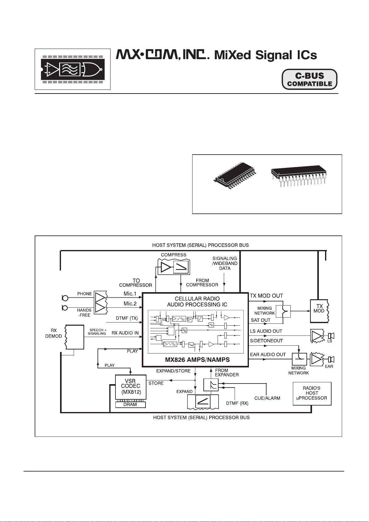
Figure1 - The MX826 AMPS/NAMPS Audio Processor Installed in a Cellular System
• HandsFree Compatibility
• Powersave (Low-Current) Settings
MX826DW MX826J
28-pin SOIC 28-pin CDIP
Page 2
AMPS/NAMPS System Audio Processor. MX826 Preliminary Information
© 1997 MX•COM Inc. www.mxcom.com Tele: 800 638-5577 910 744-5050 Fax: 910 744-5054 Doc. # 20480070.004
4800 Bethania Station Road, Winston-Salem, NC 27105-1201 USA All trademarks and service marks are held by their respective companies.
Description
The MX826 is a µProcessor controlled full-duplex
audio processor on a single-chip with separate TX and
RX paths to provide all the filter/gain/limiting functions
necessary to pre-process audio, wideband-data and SAT
cellular communications systems using the AMPS/NAMPS
or TACS/ETACS/JTACS specifications.
Selectable inputs available to the transmit path are: a
choice of two microphones and DTMF/signaling, with
access, in this path, to external compression circuitry.
Operationally the TX path provides input gain/filtering, a
deviation limiter and TX Modulation Drive controls.
In the RX path the SAT signal is separated from the
incoming audio via a filter block and made available at a
separate pin for mixing externally with the TX Modulation
Drive.
The RX path consists of an input gain/filter block for
voice, inputs from an external audio expansion system
and an output gain control driving either a loudspeaker
system or earpiece.
Unique to the MX816/826/836 cellular audio
processors is the ability to route audio (TX or RX) to an
external Voice Store and Retrieve (VSR) device such as
the MX802 or MX812 thus providing the radio system with
a voice answering and announcement facility using
external DRAM.
As a member of the DBS800 family, the MX826
follows C-BUS protocol. (C-BUS is the serial interface
used by all DBS800 integrated circuits.)
The MX826, a low-power CMOS device which reduces
the amount of microcircuits and components required in
a cellular audio system by providing more functions on a
single chip, is available in 28-pin SOIC and CDIP packages.
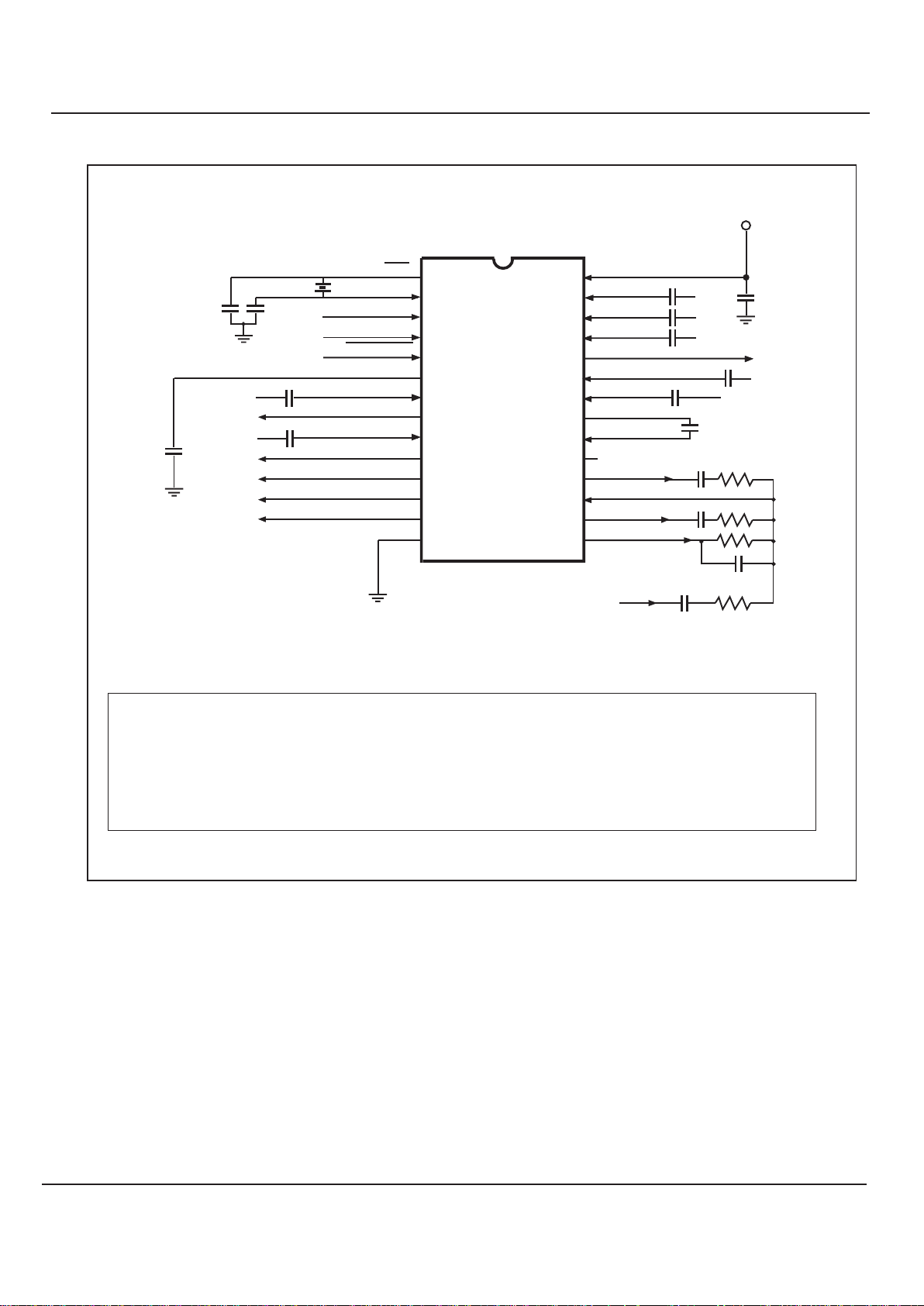
1 Xtal: The output of the on-chip clock oscillator.
2 Xtal/Clock: The input to the on-chip clock oscillator. A Xtal or externally derived clock (f
XTAL
) should be
connected here. Note that operation of the MX826 without a suitable Xtal or clock input may cause device
damage. See Figure 2 (notes).
3 Serial Clock: The “C-BUS” serial data clock input. This clock, produced by the µController, is used for
transfer timing of commands and data to the MX826. See Timing Diagrams.
4 Command Data: The “C-BUS” serial data input from the µController. Data is loaded to the MX826 in 8-
bit bytes, MSB (B7) first, and LSB (B0) last, synchronized to the Serial Clock. See Timing Diagrams.
5 Chip Select (CS): The “C-BUS” data loading control function. This input is provided by the µController.
Data transfer sequences are initiated, completed or aborted by this signal. See Timing Diagrams.
6V
BIAS
: The internal circuitry bias line, held at VDD/2 this pin must be decoupled to VSS. See Figure 2.
7 Rx Audio In: Normally taken from the radio's discriminator output, this input has a 1MΩ internal resistor
to V
BIAS
and requires to be connected via a capacitor.
8 Expand/Store: A common output that can be used as either an input to an external audio expander or
the input to a voice storage medium such as the MX812. Components relevant to the external device
requirements should be used at this output. See Figures 2 and 3.
9 (Expanded) Audio In: The audio input, via SW5, from an external expander or audio mixing function. This
input has a 1MΩ internal resistor to V
BIAS
and requires to be connected via a capacitor. See Figures 2 and
3.
10 TX Mod Out: The composite TX audio output to the transmitter modulator from a variable attenuation
stage (11H). This output is set to V
BIAS
via an internal 1MΩ resistor when set to Powersave or OFF.
11 LS Audio Out: An audio output of the Rx path (or selected audios, see Figure 3) for a loudspeaker system.
This is available for handsfree operation. This output can be connected to V
BIAS
when not required, by SW6
(Configuration Command (10H)). A driver amplifier may be required.
Notes on Inputs: To minimize aliasing effects, lowpass filtering may be required at the inputs to this device
(especially those supplied from switched-capacitor-type devices) to ensure the input spectrum is kept
below 63kHz.
Pin Function
Page 3

AMPS/NAMPS System Audio Processor. MX826 Preliminary Information
© 1997 MX•COM Inc. www.mxcom.com Tele: 800 638-5577 910 744-5050 Fax: 910 744-5054 Doc. # 20480070.004
4800 Bethania Station Road, Winston-Salem, NC 27105-1201 USA All trademarks and service marks are held by their respective companies.
12 Ear Audio Out: An audio output of the Rx path (or selected audios), available as an output for a handset
earpiece. This output, in parallel with the LS Audio Out function, can be connected to V
BIAS
when not
required, by SW7 (Configuration Command (10H)). A driver amplifier may be required.
13 Sidetone: A switched “sidetone” from the microphone inputs made available for mixing externally with
the “Ear” audio. See Figure 3.
14 VSS: Negative supply rail. Signal ground.
15 TX Mix: The output of the TX Mix Amplifier. Used with external components, it allows the TX Filter
Out output to mix with externally generated signalling tones prior to the final level adjustment.
16 SAT Out: The output of the SAT Bandpass filter. This level is recovered from the input RX audio and
is available for mixing externally with the transmitter modulation. See Figure 3.
17 TX Mix In: The input to the TX Mix Amplifier. Used with external components, it allows the TX Filter
Out output to mix with externally generated signalling tones prior to the final level adjustment. The
recovered SAT signal may be introduced at this point. See Figures 2 and 3.
18 TX Filter Out: The output of the Deviation Limiter/Lowpass Filter stage. This stage can be by-passed
using SW3 (Configuration Command). See Figure 3.
19 No internal connection – Leave open circuit.
20 Deviation Limiter In: Input to the on-chip deviation limiter. This input should be a.c. coupled to the
Pre-Emphasis Out pin. The a.c. coupling will achieve maximum possible symmetry of limiting as this
input has a 1MΩ internal resistor to V
BIAS
. See Figure 2.
21 Pre-Emphasis Out: Audio output from the TX Gain/Pre-Emphasis function. This output should be
a.c. coupled to the Deviation Limiter In pin. See Figures 2 & 3.
22 DTMF In: To introduce DTMF type audio, at a suitable level for transmission, to the TX Path,
controlled by SW2 (Configuration Command (10H)). This input has an internal 1MΩ resistor to V
BIAS
and should be connected via a capacitor.
23 Compression In: The audio input from an external compression system. This input has an internal
1MΩ resistor to V
BIAS
and should be connected via a capacitor.
24 Compression: The output to an external audio compression system. Currently available compressor/
expanders have Op-Amps incorporated. The compressor can be by-passed by SW2.
25 Mic.2 In:
26 Mic.1 In:
27 Play In: The input via SW2 from a voice storage device such as the MX812. This “replayed” audio
can be sent to RX or TX paths allowing a Messaging/Voice Notepad/Answering facility. This input has
an internal 1MΩ resistor to V
BIAS
and should be connected via a capacitor.
28 VDD: Positive supply rail. A single +5-volt power supply is required. Levels and voltages within this
Audio Processor are dependent upon this supply.
C-BUS is MX-COM’s proprietary standard for the transmission of commands and data between a
µController and the relevant Cellular microcircuits. It may be used with any µController, and can, if
desired, take advantage of the hardware serial I/O functions embodied into many types of µController .
The “C-BUS” data rate is determined solely by the µController.
Pin Function
TX voice (Mic.) inputs, selectable by SW1 available for handsfree mic./handset mic. or
any TX audio input. Pre-amplification may be required at these inputs. These inputs
each have an internal 1MΩ resistor to V
BIAS
and should be connected via a capacitor.
Page 4
AMPS/NAMPS System Audio Processor. MX826 Preliminary Information
© 1997 MX•COM Inc. www.mxcom.com Tele: 800 638-5577 910 744-5050 Fax: 910 744-5054 Doc. # 20480070.004
4800 Bethania Station Road, Winston-Salem, NC 27105-1201 USA All trademarks and service marks are held by their respective companies.
Application Information
Notes
1. Xtal/clock operation
Operation of any MX-COM IC without a Xtal or
clock input may cause device damage. To minimize
damage in the event of a Xtal/drive failure, you
should install a current limiting device (resistor or
fast-reaction fuse) on the power input (VDD).
Figure 2 - Recommended External Components
Tolerances – Capacitors ±20%
C3= 100nF
C
4
100nF
C
5
100nF
C
6
100nF
C
7
100nF
C13= 100nF
C
14
100nF
C
15
100pF
C
16
100nF
X
1
4.000MHz
R1= 100kΩ
R
2
as required
R
3
100kΩ
R
4
as required
C
1
100nF
C
2
100nF
C8= 100nF
C
9
33pF
C
10
100nF
C
11
33pF
C
12
1.0µF
2. SAT Output
It is possible, due to the impedance of this output,
that an external buffer amplifier will be required
when interfacing or mixing with other cellular system
sections.
3. TX Mix Gain
The value of R4 should be chosen with R3/C15 in
order to provide the required gain.
XTAL/CLOCK
SERIAL CLOCK
COMMAND DATA
V
BIAS
RX AUDIO IN
EXPAND/STORE
(EXPANDED) AUDIO IN
TX MOD OUT
LS AUDIO OUT
EAR AUDIO OUT
SIDETONE OUT
V
SS
SAT OUT
TX MIX IN
TX FILTER OUT
DEV LIM IN
PRE-EMP OUT
DTMF IN
(COMPRESSED) AUDIO IN
COMPRESS
MIC.2 IN
MIC.1 IN
PLAY IN
V
DD
CHIP SELECT
V
DD
XTAL
C
11
C
9
X
1
C
4
C
8
C
12
C
7
C
6
C
5
C
1
C
3
C
10
MX826J
1
2
3
4
5
6
7
8
9
10
11
12
13
14
28
27
26
25
24
23
22
21
20
19
18
17
16
15
TX MIX
C
13
C
2
Signaling and
Wideband Data
C
14
C
15
C
16
R
1
R
3
R
4
R
2
Page 5

AMPS/NAMPS System Audio Processor. MX826 Preliminary Information
© 1997 MX•COM Inc. www.mxcom.com Tele: 800 638-5577 910 744-5050 Fax: 910 744-5054 Doc. # 20480070.004
4800 Bethania Station Road, Winston-Salem, NC 27105-1201 USA All trademarks and service marks are held by their respective companies.
Figure 3 - The MX826 Internal and External Signal Paths within a AMPS/NAMPS Cellular Radio System
AMPS/NAMPS Cellular System Interfaces
INTERFACE
MOD LEVEL
MIC.2 IN
MIC.1 IN
DTMF IN
COMPRESSION IN
COMPRESSION
PLAY IN
PRE-EMP.
OUT
DEV.
LIMITER IN
TX FILTER
OUT
TX MIX
IN
TX MOD OUT
SIDETONE OUT
SAT OUT
EAR AUDIO OUT
LS AUDIO OUT
EXPAND/STORE
(EXPANDED)
AUDIO IN
SERIAL CLOCK
COMMAND DATA
SW5
SERIAL
C-BUS
and
LOGIC
BIAS
SIDETONE
BIAS
BIAS
VOLUME
SAT
XTAL/CLOCK
COMP.
BYPASS
SIDETONE
BYPASS
TX AUDIO/PLAY/STORE
SIDETONE
ENABLE
AUDIO
SELECT
SW8
#
SW7
SW6
SW4
RX Path
TX Path
SW1
SW2
XTAL
#
CLOCK
GENERATOR
DEV LIMITER
SW3
CHIP SELECT
DE-EMP
RX GAIN
dB
dB
PRE-EMP
TX GAIN ELEMENT
TX GAIN
RX GAIN ELEMENT
MX812
C-BUS
CONTROL
INPUTS
XTAL/CLOCK
COMPONENTS
(SEE FIGURE 2)
TO
MODULATOR
EXPANDER
DTMF
ALARM
EARPIECE
HANDSFREE
LOUDSPEAKER
COMPRESSOR
STORE AUDIO
MIXING
NETWORK
MIXING
NETWORK
LPF
LPF
LPF
-
+
TX MIX
V
SS
V
BIAS
V
DD
TX MIX AMP
BIAS
SIGNALING and
WIDEBAND DATA IN
FROM
DEMODULATOR
(OPTIONAL
VSR CODEC)
Mixing SAT, TX Signal & Signaling
prior to final drive adjustment...
Note that SAT & TX Mod Out may
be mixed prior to modulation.
RX AUDIO IN
HPF
HPF
SAT
BPF
Page 6

AMPS/NAMPS System Audio Processor. MX826 Preliminary Information
© 1997 MX•COM Inc. www.mxcom.com Tele: 800 638-5577 910 744-5050 Fax: 910 744-5054 Doc. # 20480070.004
4800 Bethania Station Road, Winston-Salem, NC 27105-1201 USA All trademarks and service marks are held by their respective companies.
Control Bits
Transmitted First
Sw8 Sidetone
Sidetone Bias
Sidetone Enabled
Sw6/7 RX Audio
Ear Enabled, LS Bias
LS Enabled, Ear Bias
Sw5 Expandor
Expander By-Pass
Expander Route
Sw4 TX/RX Audio
Tx Store/Audio
Rx Store/Audio
Sw3 Dev. Limiter
Dev. Limiter Bypass
Dev. Limiter Route
Sw1 Mic. Inputs
Mic. 1 Input
Mic.2 Input
Sw2 TX Function
DTMF In
Compressor Bypass
Compressor In
Play In
Setting
MSB
Bit 7
0
1
6
0
1
5
0
1
4
0
1
3
0
1
2
0
1
10
00
01
10
11
Setting
MSB
7654
0000
0001
0010
0011
0100
0101
0110
0111
1000
1001
1010
1011
1100
1101
1110
1111
3210
0000
0001
0010
0011
0100
0101
0110
0111
1000
1001
1010
1011
1100
1101
1110
1111
Gain (dBs)
Transmitted First
Tx Mod. Level
OFF (Low Z to V
BIAS
)
-5.6
-5.2
-4.8
-4.4
-4.0
-3.6
-3.2
-2.8
-2.4
-2.0
-1.6
-1.2
-0.8
-0.4
0
TX Input Gain
-2.65
-2.05
-1.50
-0.95
-0.45
0
0.45
0.85
1.25
1.65
2.05
2.40
2.70
3.05
3.35
3.65
Table 3 TX Gain & Mod. Commands
Table 2 Configuration Commands
Command Address/Command (A/C) Byte Command Table
Assignment Hex Binary Data
MSB LSB
General Reset 01 00000001
Configuration Command 10 00010000 + 1 byte 2
TX Gain & Mod. Command 11 00010001 + 1 byte 3
RX Gain & Vol. Command 12 00010010 + 1 byte 4
Powersave Command 13 00010011 + 1 byte 5
Table 1 “C-Bus” Address/Commands
Configuration Command
(
Preceded by A/C 10H)
TX Gain & Mod. Command
(Preceded by A/C 11H)
In C-BUS protocol the audio processor is allocated
Address/Command (A/C) values 10
H
to 13H. Configuration, TX/
RX Gains, Powersave assignments and data requirements are
given in Table 1. Each instruction consists of an Address/
Command (A/C) byte followed by a data instruction formulated
from the following tables.
Commands and Data are only to be loaded in the group
configurations detailed, as the C-BUS interface recognizes the
first byte after Chip Select (logic “0”) as an Address/Command.
Function or Level control data, which is detailed in Tables 2, 3,
4 and 5, is acted upon at the end of the loaded instruction. See
Timing Diagrams, Figures 5 and 6.
Upon Power-Up the value of the “bits” in this device will be
random (either “0” or “1”). A General Reset Command (01
H
)
will be required to set all MX826 registers to 00H.
The Controlling System: C-BUS Hardware Interface
C-BUS is MX-COM's proprietary standard for the transmission of commands and data between a µController and MXCOM's New Generation integrated circuits. C-BUS has been designed for a low IC pin-count, flexibility in handling variable
amounts of data, and simplicity of system design and µController software.
It may be used with any µController, and can, if desired, take advantage of the hardware serial I/O functions built into
many types of µController. Because of this flexibility and because the BUS data-rate is determined solely by the
µController, the system designer has complete freedom to choose a µController appropriate to the overall system
processing requirements.
Control of the functions and levels within the MX826 is by a group of Address/Commands and appended data
instructions from the system µController to set/adjust the functions and elements of the device. The use of these
instructions is detailed in the following paragraphs and tables.
Page 7

AMPS/NAMPS System Audio Processor. MX826 Preliminary Information
© 1997 MX•COM Inc. www.mxcom.com Tele: 800 638-5577 910 744-5050 Fax: 910 744-5054 Doc. # 20480070.004
4800 Bethania Station Road, Winston-Salem, NC 27105-1201 USA All trademarks and service marks are held by their respective companies.
Figure 4 - Signal Deviation Levels and corresponding TX Mod Outputs with the Mod Level set to 0dB
Reference Signal Levels
Gain (dBs)
Transmitted First
RX Volume
OFF (Low Z to V
BIAS
)
-28.0
-26.0
-24.0
-22.0
-20.0
-18.0
-16.0
-14.0
-12.0
-10.0
-8.0
-6.0
-4.0
-2.0
0
RX Input Gain
3.75
4.30
4.80
5.30
5.80
6.20
6.55
7.05
7.40
7.80
8.15
8.50
8.80
9.10
9.40
9.70
Setting
MSB
7654
0000
0001
0010
0011
0100
0101
0110
0111
1000
1001
1010
1011
1100
1101
1110
1111
3210
0000
0001
0010
0011
0100
0101
0110
0111
1000
1001
1010
1011
1100
1101
1110
1111
Table 4 - RX Gain and Vol. Commands
The Controlling System ......
RX Gain & Vol. Command
(
Preceded by A/C 12H)
Control Bits
Transmitted First
All must be a logic “0”
Powersave Setting
Powersave MX826
Enable MX826
Setting
MSB
Bit 7
7654321
0000000
0
0
1
Powersave Command
(Preceded by A/C 13H)
Table 5 - Powersave Command
10
20
103 1.9
30
40
50
60
70
80
90
100
%kHz
mV
(rms)
Signaling
Tone
10kHz
and WBD
205 3.8
308 5.7
411 7.6
513 9.5
DEVIATION (+/-)
1.0kHz
Tone
24.2%
2.3kHz
125mV
Maximum
Deviation
100%
9.5kHz
513mV
SATTone
5970kHz
6000kHz
6030kHz
17.9%
1.7kHz
92mV
Normal
Test
Modulation
67.4%
6.4kHz
346mV
Min.
697Hz
60.0%
5.7kHz
308mV
Max.
1633Hz
12.6%
1.2kHz
65mV
37.1%
3.52kHz
190mV
DTMF
Page 8

AMPS/NAMPS System Audio Processor. MX826 Preliminary Information
© 1997 MX•COM Inc. www.mxcom.com Tele: 800 638-5577 910 744-5050 Fax: 910 744-5054 Doc. # 20480070.004
4800 Bethania Station Road, Winston-Salem, NC 27105-1201 USA All trademarks and service marks are held by their respective companies.
Figure 6 - Control Timing Relationships
Figure 5 - Control Timing Information
Control Timing Information
Characteristics See Note Min. Typ. Max. Unit
t
CSE
“CS-Enable to Clock-High” 1 2.0 – – µs
t
CSH
Last “Clock-High to CS-High” 1 4.0 – – µs
t
CSOFF
“CS-High” Time between transactions 1, 2 2.0 – – µs
t
CK
“Clock-Cycle” Time 1 2.0 – – µs
t
NXT
“Inter-Byte” Time 1 4.0 – – µs
t
CH
“Serial Clock-High” Period 500 – – ns
t
CL
“Serial Clock-Low” Period 500 – – ns
t
CDS
“Command Data Set-Up” Time 250 – – ns
t
CDH
“Command Data Hold” Time 0 – – ns
Notes
1. These Minimum Timing values are altered during operation of the MX812 VSR Codec.
2. Chip Select must be taken to a logic “1” between each individual transaction.
➤
➤
➤
➤
➤
➤
➤
➤
➤
➤
➤
➤
➤
➤
➤
➤
➤
➤
➤
➤
Page 9

AMPS/NAMPS System Audio Processor. MX826 Preliminary Information
© 1997 MX•COM Inc. www.mxcom.com Tele: 800 638-5577 910 744-5050 Fax: 910 744-5054 Doc. # 20480070.004
4800 Bethania Station Road, Winston-Salem, NC 27105-1201 USA All trademarks and service marks are held by their respective companies.
Frequency Responses
Figure 7 - Microphone Input Stages -Combined Low and Highpass Filter Frequency Response
Figure 7
Mic.1/2 In to Compression Out
V
DD
= 5.0V
Signal Input Level = 55.0mVrms
Figure 8
Dev Limiter In to TX Filter Out
V
DD
= 5.0V
Signal Input Level = 55.0mVrms
Figure 9 - RX SAT Path Bandpass Filter Response
Figure 8 - Post Deviation Limiter Lowpass Filter Response
Figure 9
RX Audio In to SAT out
V
DD
= 5.0V
Signal Input Level = 100mVrms
100030010050
-40
-30
dB
-20
-10
0
10
3000 10000
Frequency (Hz)
dB
-50
-40
-30
-20
-10
0
10
Frequency (Hz)
2000
3000
4000
6000
10000
3000
-50
-40
-30
-20
20
-10
0
10
6000
10000
Frequency (Hz)
dB
Page 10

AMPS/NAMPS System Audio Processor. MX826 Preliminary Information
© 1997 MX•COM Inc. www.mxcom.com Tele: 800 638-5577 910 744-5050 Fax: 910 744-5054 Doc. # 20480070.004
4800 Bethania Station Road, Winston-Salem, NC 27105-1201 USA All trademarks and service marks are held by their respective companies.
Characteristics See Note Min. Typ. Max. Unit
Static Values
Supply Voltage 4.5 5.0 5.5 V
Supply Current
Operating – 6.5 – m A
Powersave – 0.5 – m A
Alias Frequency – 63.0 – kHz
On-Chip Xtal Oscillator
R
IN
10.0 – – MΩ
R
OUT
– 10.0 – kΩ
Inverter d.c. Voltage Gain – 10.0 – V/V
Gain/Bandwidth Product – 10.0 – MHz
TX Mix Amp (Open Loop Gain) – 50.0 – dB
(Bandwidth) 20.0 – – kHz
Analog Input Impedances
Mic.1 & 2 – 500 – kΩ
Play – 500 – kΩ
Comp In – 500 – kΩ
DTMF In – 500 – kΩ
Dev. Limiter In – 100 – kΩ
(Expanded) Audio In – 47.0 – kΩ
TX Mix In 10.0 – – MΩ
RX Audio In – 100 – kΩ
Analog Output Impedances
Pre-Emp Out – 600 – Ω
TX Mod Out – 600 – Ω
Expand/Store – 600 – Ω
LS and Ear Audio – 1.0 – kΩ
SAT Out 3 – 1.0 – kΩ
TX Filter Out – 600 – Ω
Comp Out – 600 – Ω
Sidetone Out – 2.0 – kΩ
TX Mix (Open Loop) – 6.0 – kΩ
(Closed Loop) – 600 – Ω
Switches – ON – 1.0 – kΩ
– OFF 10.0 – – MΩ
Specifications
Absolute Maximum Ratings
Exceeding the maximum rating can result in device
damage. Operation of the device outside the operating
limits is not suggested.
Supply Voltage -0.3 to 7.0 V
Input Voltage at any pin
(Ref VSS = 0V) -0.3V to (VDD + 0.3V)
Sink/source Current
(Supply pins) ±30mA
(Other pins) ±20mA
Total Device Dissipation
@T
AMB
25°C 800mW max.
Derating 10mW/°C
Operating Temperature -40°C to +85°C
Storage Temperature -55°C to +125°C
Operating Limits
All devices were measured under the following
conditions unless otherwise noted.
VDD = 5.0V
T
AMB
= 25°C
Xtal/clock f
XTAL
= 4.0MHz
Audio level 0dB ref. = 308mVrms @ 1kHz
Page 11

AMPS/NAMPS System Audio Processor. MX826 Preliminary Information
© 1997 MX•COM Inc. www.mxcom.com Tele: 800 638-5577 910 744-5050 Fax: 910 744-5054 Doc. # 20480070.004
4800 Bethania Station Road, Winston-Salem, NC 27105-1201 USA All trademarks and service marks are held by their respective companies.
Characteristics See Note Min. Typ. Max. Unit
Control Interface Parameters
Input Logic Levels
Logic “1” 1 3 .5 – – V
Logic “0” 1 – – 1.5 V
IIN (logic “1” or “0”) 1 -1.0 – 1.0 µA
Input Capacitance 1 – – 7.5 pF
Channel Performances
TX Path
Filter Specifications
Pre-Compression L/HPF Combination
Passband 300 3000 Hz
Slope - below 300Hz +24.0 – – dB/oct.
above 3000Hz -24.0 – – dB/oct.
TX Gain Pre-Emphasis
Gain at 1.0kHz – 0 – dB
Slope (300Hz - 3000Hz) – 6.0 – dB/oct.
Post Deviation Limiter LPF
Attenuation Relative to 1.0kHz
3.0kHz - 5.9kHz - 40 log(f/3000) - dB
5.9kHz - 6.1kHz - 35.0 - dB
6.1kHz - 15kHz - 40 log(f/3000) - dB
>15kHz - 28.0 - dB
Analog Signal Input Levels
Mic. 1 and 2 2 – 0 – dB
Play 2 – 0 – dB
DTMF 2 – 0 – dB
Comp. In 2 – 0 – dB
TX Mix In 2 – 0 – dB
Analog Signal Output Levels
Pre-Emp Out 2 – 0 – dB
TX Filter Out 2 – 0 – dB
TX Mod Out 2 – 0 – dB
Sidetone Out 2 – 0 – dB
Path Gains/Levels
TX Gain – 11
H
Nominal Adjustment Range -2.65 – 3.65 dB
Error of any Setting -0.2 – 0.2 dB
Dev Limiter
Threshold – 1086 – mVp-p
Symmetry – 7.0 – %
Mod Level Attenuation – 11
H
Nominal Adjustment Range -5.6 0 dB
Step Size 0.2 0.4 0.6 dB
Error of any Setting -1.0 – 1.0 dB
Overall
TX Distortion – -40.0 -32.0 dBp
TX Hum and Noise – -40.0 -20.0 dB
RX Signal Path
Filter Specifications
RX Gain De-Emphasis
Gain at 1.0kHz – 3.75 – dB
Slope (300Hz - 3000Hz) – -6.0 – dB/oct.
RX Channel Bandpass 300 3000 Hz
Slope - below 300Hz +24.0 – – dB/oct.
above 3000Hz -36.0 – – dB/oct.
Page 12

AMPS/NAMPS System Audio Processor. MX826 Preliminary Information
© 1997 MX•COM Inc. www.mxcom.com Tele: 800 638-5577 910 744-5050 Fax: 910 744-5054 Doc. # 20480070.004
4800 Bethania Station Road, Winston-Salem, NC 27105-1201 USA All trademarks and service marks are held by their respective companies.
RX Signal Path (cont'd)
Analog Signal Levels
RX Audio Input Level 2 – -7.0 – dB
LS/Ear Audio Output Level 2 – 0–dB
Path Gains/Levels
RX Gain – 12
H
Nominal Adjustment Range 3.75 9.70 dB
Error of any Setting -0.2 – 0.2 dB
Volume – 12
H
Nominal Adjustment Range -28.0 0 dB
Step Size 1.5 2.0 2.5 dB
Error of any Setting -1.0 – 1.0 dB
Overall
RX Distortion – -40.0 -32.0 dBp
RX Hum and Noise – -40.0 -34.0 dB
SAT Signal Path
Bandpass Filter
Frequency Range 5970 6030 Hz
Gain 19.0 20.0 21.0 dB
Notes
1. Serial Clock, Command Data and Chip Select inputs.
2. Levels equivalent to ±3.0kHz deviation with the settings below:
TX Gain = 0dB Mod Level = 0dB
RX Gain = 7.05dB Volume = 0dB
Other levels can be achieved by adjusting the above variable gain blocks in accordance with
Tables 1 to 5.
3. Recommended load >10.0kΩ.
Characteristics See Note Min. Typ. Max. Unit
Page 13

AMPS/NAMPS System Audio Processor. MX826 Preliminary Information
© 1997 MX•COM Inc. www.mxcom.com Tele: 800 638-5577 910 744-5050 Fax: 910 744-5054 Doc. # 20480070.004
4800 Bethania Station Road, Winston-Salem, NC 27105-1201 USA All trademarks and service marks are held by their respective companies.
Package Outline
The MX826 packages available are shown below. Pin 1
is marked with an indent spot. Pins on both package
styles number counter-clockwise when viewed from the
top (marked side).
Handling Precautions
The MX826 is a CMOS LSI circuit which includes input
protection. However precautions should be taken to
prevent static discharges which may cause damage.
R
P
J
J
K
M
L
N
➤
➤
➤
➤
A
B
➤
➤
➤
➤
➤
➤
➤
➤
➤
➤
➤
➤
➤➤
➤
➤
➤
➤
➤
➤
➤
➤
➤
➤
➤
➤➤
F
G
E
C
H
D
PackageTolerances
Fig.10 MX826DW 28-pin Small Outline I.C. Package
➤
➤
➤
➤
➤
➤
J
K
L
➤
➤
➤
➤
A
A
B
➤
➤
➤
➤
➤
➤
➤
➤
➤
➤
➤
➤
➤
E
F
G
C
D
H
H
Package T oler ances
Fig.11 MX826J 28-pin Ceramic Dual In-Line Package
 Loading...