

Page 1
MYSON
8051 core, 12MHz operating frequency.
1024-byte RAM, 64K-byte
Maximum 14 channels of 9V open-drain PWM DAC.
Watchdog timer with prog
FIFOs), the other one is Interrupt endpoint (8-byte IN FIFO).
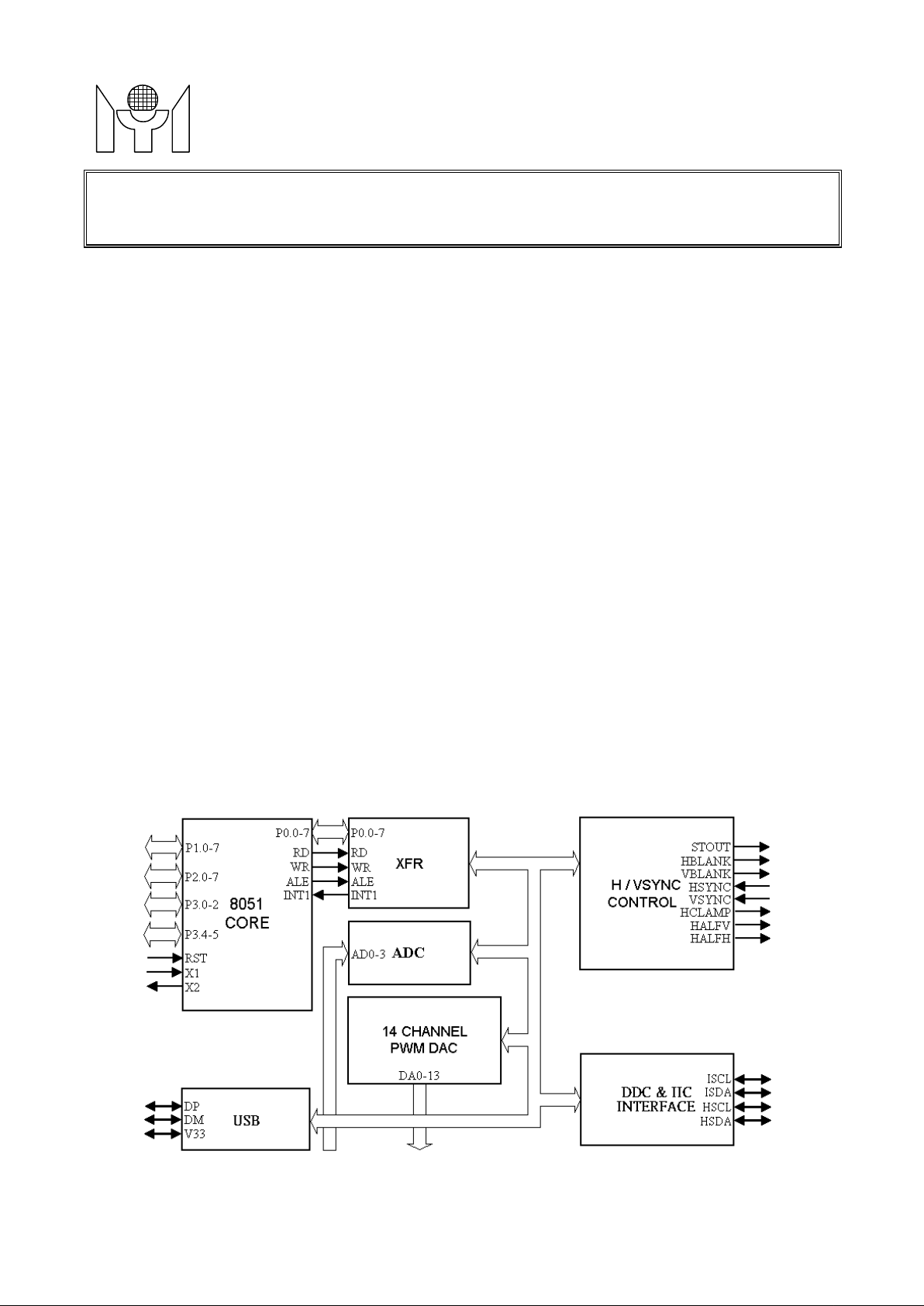
applications. It includes an 8051 CPU core, 1024-byte SRAM, SYNC process or, 14 built-in PWM DACs,
MTV212M64
TECHNOLOGY
(Rev. 1.2)
8051 Embedded Monitor Controller
MTP Type
FEATURES
•
•
•
• Maximum 32 bi-directional I/O pins.
• SYNC processor for composite separation/insertion, H/V polarity/frequency check, polarity adjustment
and programmable clamp pulse output.
• Built-in self-test pattern generator with three free-running timings.
• Built-in low power reset circuit.
• Compliant with VESA DDC1/2B/2Bi/2B+ standard.
• Dual slave IIC addresses.
• Single master IIC interface for internal device communication.
• 4-channel 6-bit ADC.
•
• Compliant with Low Speed USB Spec.1.1 including 2 Endpoints: one is Control endp oint (8-byte IN & 8-
byte OUT
• Built-in 3.3V regulator for USB Interface.
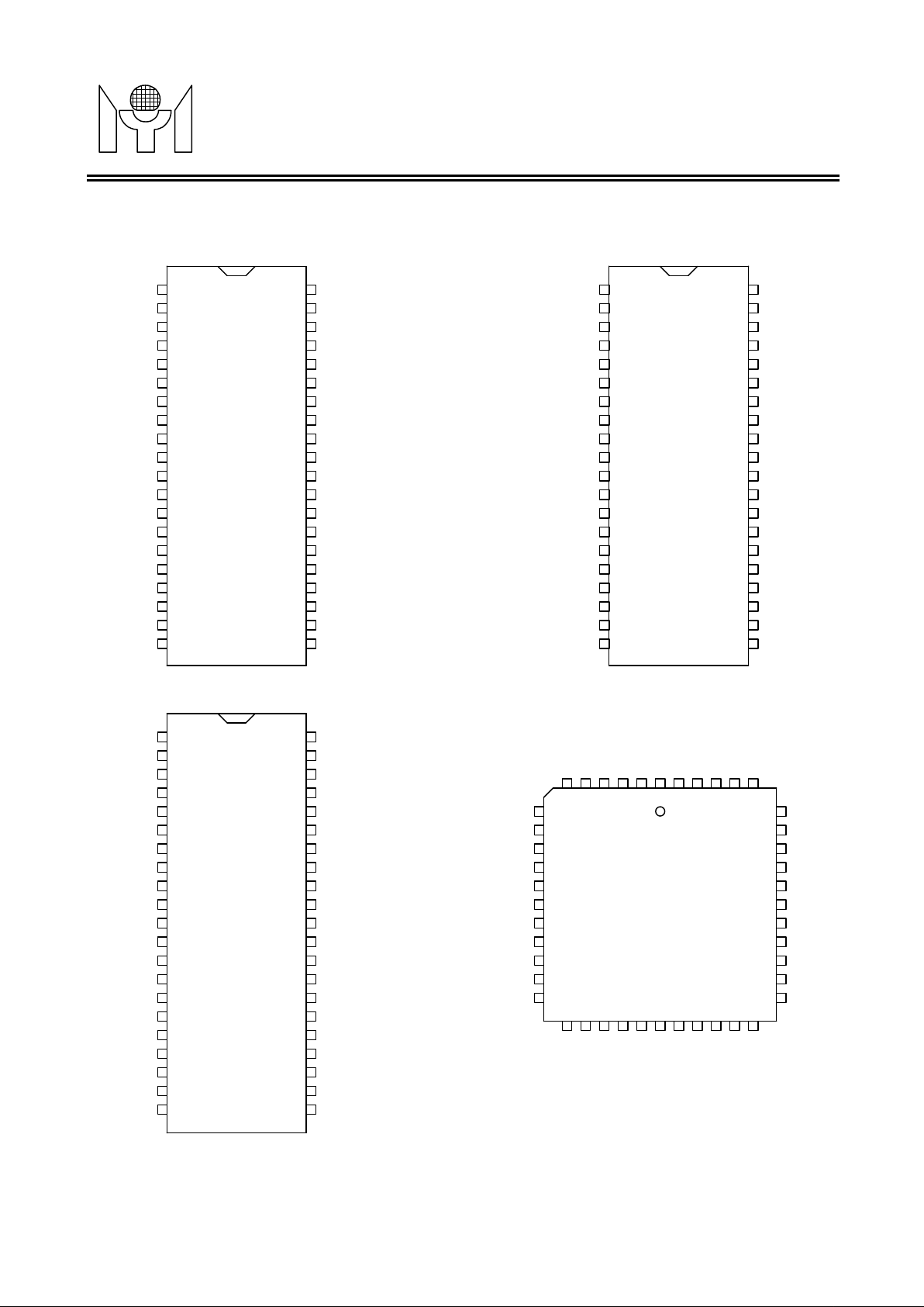
• 40-pin DIP, 42-pin SDIP or 44-pin PLCC package.
program Flash-ROM.•
rammable interval.
GENERAL DESCRIPTIONS
The MTV212M micro-controller is an 8051 CPU core embedded device specially tailored to Monitor
VESA DDC interface, 4-channel A/D converter, Low Speed USB Interface and a 64K-byte internal program
Flash-ROM.
BL OCK DIAGRAM
This datasheet contains new product information. Myson Technology reserves the rights to modify the product specification without
notice. No liability is assumed as a result of the use of this product. No rights under any patent accompany the sale of the product.
Revision 1.2 - 1 - 2000/07/04
Page 2

MYSON
Auxiliary RAM (AUXRAM)
MTV212M64
TECHNOLOGY
(Rev. 1.2)
DEVICE SUMMARY
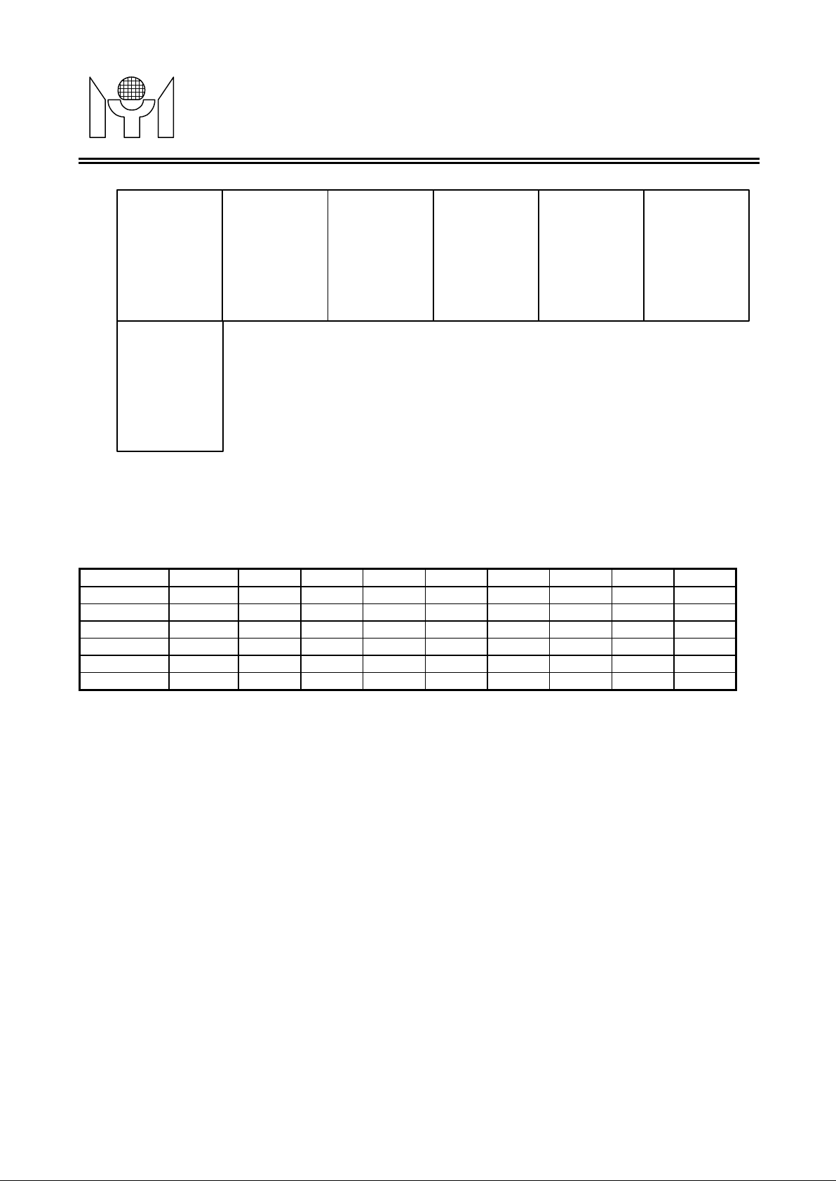
The MTV212M is the MTP (Multi-Time Programming) type device for all of MTV212A mask ROM derivatives,
the memory size and package differences please see the table below:
Part Numb er USB ROM RAM Pack ag e
MTV212A16 No 16K 256 PDIP40, SDIP42, PLCC44
MTV212A24 No 24K 512 PDIP40, SDIP42, PLCC44
MTV212A32 No 32K 512 PDIP40, SDIP42, PLCC44
MTV212A32U Yes 32K 768 PDIP40, SDIP42, PLCC44
MTV212A48U Yes 48K 768 PDIP40, SDIP42, PLCC44
MTV212A64U Yes 64K 1024 PDIP40, SDIP42, PLCC44
The use of
selection is defined as the table below:
Part Numb er RAM Xbnk2 Xbnk1 Xbnk 0
MTV212A16 256 - - MTV212A24 512 0 0 0
0 0 1
MTV212A32 512 0 0 0
0 0 1
MTV212A32U 768 0 0 0
MTV212A48U 768 0 0 0
MTV212A64U 1024 0 0 0
is limited for targeted mask ROM, the allowable XBANK (35h) bank
0 0 1
0 1 0
0 1 1
0 0 1
0 1 0
0 1 1
0 0 1
0 1 0
0 1 1
1 0 0
1 0 1
Remark:
The major pin connection differences between USB (MTV212M64U) and non-USB (MTV212M64) types are
pin# 4, #5 and #6 for SDIP42 and PLCC44. The pin name of USB device is V33CAP(#4), VM(#5) and
VP(#6), while NC (No Connection) for non-USB device.
Revision 1.2 - 2 - 2000/07/04
Page 3
MYSON
DA2/P5.2
DA1/P5.1
DA0/P5.0
VSS
ISDA/P3.4/T0
ISCL/P3.5/T1
STOUT/P4.2
P2.2/AD2
P3.2/INT0
DA2/P5.2
DA1/P5.1
DA0/P5.0
VSS
ISDA/P3.4/T0
ISCL/P3.5/T1
STOUT/P4.2
P2.2/AD2
P3.2/INT0
Non-USB
DA2/P5.2
DA1/P5.1
DA0/P5.0
VSS
ISDA/P3.4/T0
ISCL/P3.5/T1
STOUT/P4.2
P2.2/AD2
P3.2/INT0
V33CAP/NC
P1.624P1.7
P2.1/AD1
P1.5
P2.0/AD0
HSDA/P3.1/Txd
P1.1
P3.2/INT0
P1.2
P1.3
P1.4
23222120282726
25
DP/NC
6543214443424140
DM/NC
V33CAP/NC
DA0/P5.0
DA1/P5.1
DA2/P5.2
VSYNC
HSYNC
DA3/P5.3
DA4/P5.4
DA5/P5.5
19
18
VSS
ISDA/P3.4/T0
ISCL/P3.5/T1
STOUT/P4.2
P2.2/AD2
P2.3/AD3
MTV212M64
TECHNOLOGY
PIN CONNECTION
2
3
4
RST
5
VDD
6
7
X2
8
X1
P1.0
P1.1
P1.2
P1.3
P1.4
P1.5
P1.6
9
10
11
12
13
14
15
16
17
18
19
20
MTV212M
40 Pin
PDIP #1
Non-USB
401
VSYNC
39
HSYNC
38
DA3/P5.3
37
DA4/P5.4
36
DA5/P5.5
35
DA8/HALFH
34
DA9/HALFV
33
HBLANK/P4.1
32
VBLANK/P4.0
31
DA7/HCLAMP
30
DA6/P5.6
29
P2.7/DA13
28
P2.6/DA12
27
P2.5/DA11
26
P2.4/DA10
25
HSCL/P3.0/Rxd
24
HSDA/P3.1/Txd
23
P2.0/AD0
22
P2.1/AD1
21
P1.7
V33CAP
DM
DP
RST
VDD
X2
X1
P1.0
P1.1
P1.2
P1.3
2
3
4
5
6
7
8
9
10
11
12
13
14
15
16
17
18
19
20
MTV212M
40 Pin
PDIP #2
USB
(Rev. 1.2)
401
VSYNC
39
HSYNC
38
DA3/P5.3
37
DA4/P5.4
36
DA5/P5.5
35
DA8/HALFH
34
DA9/HALFV
33
HBLANK/P4.1
32
VBLANK/P4.0
31
DA7/HCLAMP
30
DA6/P5.6
29
P2.4/DA10
28
HSCL/P3.0/Rxd
27
HSDA/P3.1/Txd
26
P2.0/AD0
25
P2.1/AD1
24
P1.7
23
P1.6
22
P1.5
21
P1.4
DM/NC
DP/NC
RST
VDD
X2
X1
P1.0
P1.1
P1.2
P1.3
P1.4
1
2
3
4
5
6
7
8
9
10
11
12
13
14
15
16
17
18
19
20
MTV212M
42 Pin
SDIP
USB
or
VSYNC
42
HSYNC
41
40
DA3/P5.3
39
DA4/P5.4
38
DA5/P5.5
37
DA8/HALFH
36
DA9/HALFV
35
HBLANK/P4.1
34
VBLANK/P4.0
33
DA7/HCLAMP
32
DA6/P5.6
31
P2.6/DA12
30
P2.5/DA11
29
P2.4/DA10
28
HSCL/P3.0/Rxd
27
HSDA/P3.1/Txd
26
P2.0/AD0
25
P2.1/AD1
24
P1.7
23
P1.6
2221
P1.5
RST
VDD
X2
X1
P1.0
7
8
9
10
11
12
13
14
15
16
17
MTV212M
44 Pin
PLCC
USB
or
Non-USB
39
DA8/HALFH
38
DA9/HALFV
37
HBLANK/P4.1
36
VBLANK/P4.0
35
DA7/HCLAMP
34
DA6/P5.6
33
P2.7/DA13
32
P2.6/DA12
31
P2.5/DA11
30
P2.4/DA10
29
HSCL/P3.0/Rxd
Revision 1.2 - 3 - 2000/07/04
Page 4

MYSON
PWM DAC output / Hsync clamp pulse output (open drain).
PWM DAC output /
PWM DAC output / Hsync half freq. output (open drain).
MTV212M64
TECHNOLOGY
PIN DESCRIPTION
Name Type
DA2/P5.2
DA1/P5.1
DA0/P5.0
V33CAP/NC
DM/NC
DP/NC
RST
VDD
P2.3/AD3
VSS
X2
X1
ISDA/P3.4/T0
ISCL/P3.5/T1
STOUT/P4.2
P2.2/AD2
P1.0
P1.1
P3.2/INT0
P1.2
P1.3
P1.4
P1.5
P1.6
P1.7
P2.1/AD1
P2.0/AD0
HSDA/P3.1/Txd
HSCL/P3.0/Rxd
P2.4/DA10
P2.5/DA11
P2.6/DA12
P2.7/DA13
DA6/P5.6
DA7/HCLAMP
VBL ANK /P4.0
HBLA NK /P4.1
DA9/HALFV
DA8/HALFH
DA5/P5.5
DA4/P5.4
DA3/P5.3
HSYNC
VSYNC
I/O 1 1 1 1 PWM DAC output / General purpose I/O (open drain).
I/O 2 2 2 2 PWM DAC output / General purpose I/O (open drain).
I/O 3 3 3 3 PWM DAC output / General purpose I/O (open drain).
I/O - 4 4 4 3.3V Regulator Capacitor connection or N C.
I/O - 5 5 5 USB DM or NC.
I/O - 6 6 6 USB DP or NC.
I/O - - - 9 General purpose I/O / ADC Input.
I/O 9 12 12 13 Master IIC data / General purpose I/O / T 0.
I/O 10 13 13 14 Master IIC clock / General purpose I/O / T1.
I/O 12 15 15 16 General purpose I/O / ADC Input.
I/O 13 16 16 17 General purpose I/O.
I/O 14 17 17 18 General purpose I/O.
I/O 16 19 19 20 General purpose I/O.
I/O 17 20 20 21 General purpose I/O.
I/O 18 21 21 22 General purpose I/O.
I/O 19 22 22 23 General purpose I/O.
I/O 20 23 23 24 General purpose I/O.
I/O 21 24 24 25 General purpose I/O.
I/O 22 25 25 26 General purpose I/O / ADC Input.
I/O 23 26 26 27 General purpose I/O / ADC Input.
I/O 24 27 27 28 Slave IIC data / General purpose I/O / Txd.
I/O 25 28 28 29 Slave IIC clock / General purpose I/O / Rxd.
I/O 26 29 29 30 General purpose I/O / PWM DAC output (open drain).
I/O 27 - 30 31 General purpose I/O / PWM DAC output (open drain).
I/O 28 - 31 32 General purpose I/O / PWM DAC output (open drain).
I/O 29 - - 33 General purpose I/O / PWM DAC output (open drain).
I/O 30 30 32 34 PWM DAC output / General purpose I/O (open drain).
I/O 36 36 38 40 PWM DAC output / General purpose I/O (open drain).
(Rev. 1.2)
Pin#
40 40 42 44
I 4 7 7 7 Active high reset.
- 5 8 8 8 Positive Power Supply.
- 6 9 9 10 Ground.
O 7 10 10 11 Oscillator output.
I 8 11 11 12 Oscillator input.
O 11 14 14 15 Self-test video output / General purpose Output.
I 15 18 18 19 General purpose Input / INT0.
O 31 31 33 35
O 32 32 34 36 Vertical blank / General purpose Output.
O 33 33 35 37 Horizontal blank / General purpose Output.
O 34 34 36 38
O 35 35 37 39
O 37 37 39 41 PWM DAC output / General purpose I/O (open drain).
O 38 38 40 42 PWM DAC output / General purpose I/O (open drain).
I 39 39 41 43 Horizontal SYNC or Composite SYNC Input.
I 40 40 42 44 Vertical SYNC input.
Description
Vsync half freq. output (open drain).
Revision 1.2 - 4 - 2000/07/04
Page 5

MYSON
FUNCTIONAL DESCRIPTIONS
2. Memory Allo catio n
used for monitor control or PWM DAC. Program can initialize
2.4 Auxiliary RAM (AUXRAM)
divided into six banks, selected by XBANK register. Program can initialize Ri value and use "MOVX"
MTV212M64
TECHNOLOGY
1. 8051 CPU Core
MTV212M includes all 8051 functions with the following exceptions:
1.1 PSEN, ALE, RD and WR pins are disabled. The external RAM access is restr icted to XFRs within the
MTV212M.
1.2 Port0, port3.3, port3.6 and port3.7 are not general-purpose I/O ports. They are dedicated to monitor
special application.
1.3 INT1 input pin is not provided, it is connected to special interrupt sources.
1.4 Port2 are shared with special function pins.
In addition, there are 2 timers, 5 interrupt sources and serial interface compatible with the standard 8051.
(Rev. 1.2)
Note: All registers listed in this document reside in external RAM area (XFR). For internal RAM memory map
please refer to 8051 spec.
2.1 Internal Special Function Registers (SFR)
The SFR is a group of registers that are the same as standard 8051.
2.2 Internal RAM
There are total 256 bytes internal RAM in MTV212M, same as standard 8052.
2.3 External Special Function Registers (XFR)
The XFR is a group of registers allocated in the 8051 external RAM area 00h - 7Fh. Most of the registers are
Ri value and use "MOVX" instruction to access
these registers.
There are total 768 bytes auxiliary RAM allocated in the 8051 external RAM area 80h - FFh. The AUXRAM is
instruction to access the AUXRAM.
FFh
Internal RAM
Accessible by
addressing only
MOV A,@Ri
instruction)
80h
7Fh
Internal RAM
Accessible by
direct and indirect
addressing
indirect
(Using
SFR
Accessible by
direct addressing
00h
Revision 1.2 - 5 - 2000/07/04
Page 6
MYSON
PWMF
MTV212M64
(Rev. 1.2)
AUXRAM
Accessible by
indirect external
RAM addressing
(XBANK=5)(Using
MOVX A,@Ri
instruction)
FFh
80h
7Fh
00h
AUXRAM
Accessible by
indirect external
RAM addressing
(XBANK=0)(Using
MOVX A,@Ri
instruction)
Accessible by
indirect external
RAM addressing
MOVX A,@Ri
instruction
XFR
(Using
TECHNOLOGY
AUXRAM
Accessible by
indirect external
RAM addressing
(XBANK=1)(Using
MOVX A,@Ri
instruction)
AUXRAM
Accessible by
indirect external
RAM addressing
(XBANK=2)(Using
MOVX A,@Ri
instruction)
AUXRAM
Accessible by
indirect external
RAM addressing
(XBANK=3)(Using
MOVX A,@Ri
instruction)
AUXRAM
Accessible by
indirect external
RAM addressing
(XBANK=4)(Using
MOVX A,@Ri
instruction)
3. Chip Configu ratio n
The Chip Configuration registers define the chip pins function, as well as the functional blocks' connection,
configuration and frequency.
Reg name addr bit7 bit6 bit5 bit4 bit3 bit2 bit1 bit0
PADMOD
PADMOD
PADMOD
OPTION
OPTION
XBANK
30h (w) DA13E DA12E DA11E DA10E AD3E AD2E AD1E AD0E
31h (w) P56E P55E P54E P53E P52E P51E P50E
32h (w) HIICE IIICE HLFVE HLFHE HCLPE P42E P41E P40E
33h (w)
DIV253 FclkE IICpass ENSCL Msel MIICF1 MIICF0
34h (w) SlvAbs1 SlvAbs0
35h (r/w) Xbnk2 Xbnk1 Xbnk0
PADMOD (w) : Pad mode control registers. (All are "0" in Chip Reset)
DA13E = 1 → pin “P2.7/DA13” is DA13.
= 0 → pin “P2.7/DA13” is P2.7.
DA12E = 1 → pin “P2.6/DA12” is DA12.
= 0 → pin “P2.6/DA12” is P2.6.
DA11E = 1 → pin “P2.5/DA11” is DA11.
= 0 → pin “P2.5/DA11” is P2.5.
DA10E = 1 → pin “P2.4/DA10” is DA10.
= 0 → pin “P2.4/DA10” is P2.4.
AD3E = 1 → pin “P2.3/AD3” is AD3.
= 0 → pin “P2.3/AD3” is P2.3.
AD2E = 1 → pin “P2.2/AD2” is AD2.
= 0 → pin “P2.2/AD2” is P2.2.
AD1E = 1 → pin “P2.1/AD1” is AD1.
= 0 → pin “P2.1/AD1” is P2.1.
AD0E = 1 → pin “P2.0/AD0” is AD0.
= 0 → pin “P2.0/AD0” is P2.0.
P56E = 1 → pin “DA6/P5.6” is P5.6.
= 0 → pin “DA6/P5.6” is DA6.
P55E = 1 → pin “DA5/P5.5” is P5.5.
= 0 → pin “DA5/P5.5” is DA5.
Revision 1.2 - 6 - 2000/07/04
Page 7

MYSON
is HSYNC half frequency output.
is HSYNC clamp pulse output.
Auxiliary RAM bank switch.
MTV212M64
TECHNOLOGY
P54E = 1 → pin “DA4/P5.4” is P5.4.
= 0 → pin “DA4/P5.4” is DA4.
P53E = 1 → pin “DA3/P5.3” is P5.3.
= 0 → pin “DA3/P5.3” is DA3.
P52E = 1 → pin “DA2/P5.2” is P5.2.
= 0 → pin “DA2/P5.2” is DA2.
P51E = 1 → pin “DA1/P5.1” is P5.1.
= 0 → pin “DA1/P5.1” is DA1.
P50E = 1 → pin “DA0/P5.0” is P5.0.
= 0 → pin “DA0/P5.0” is DA0.
HIICE = 1 → pin “HSCL/P3.0/Rxd” is HSCL; pin “HSDA/P3.1/Txd” is HSDA.
= 0 → pin “HSCL/P3.0/Rxd” is P3.0/Rxd; pin “HSDA/P3.1/Txd” is P3.1/Txd.
IIICE = 1 → pin “ISDA/P3.4/T0” is ISDA; pin “ISCL/P3.5/T1” is ISCL.
= 0 → pin “ISDA/P3.4/T0” is P3.4/T0; pin “ISCL/P3.5/T1” is P3.5/T1.
HLFVE = 1 → pin “DA9/HALFV” is VSYNC half frequency output.
= 0 → pin “DA9/HALFV” is DA9.
HLFHE = 1 → pin “DA8/HALFH”
= 0 → pin “DA8/HALFH” is DA8.
HCLPE = 1 → pin “DA7/HCLAMP”
= 0 → pin “DA7/HCLAMP” is DA7.
P42E = 1 → pin “STOUT/P4.2” is P4.2.
= 0 → pin “STOUT/P4.2” is STOUT.
P41E = 1 → pin “HBLANK/P4.1” is P4.1.
= 0 → pin “HBLANK/P4.1” is HBLANK.
P40E = 1 → pin “VBLANK/P4.0” is P4.0.
= 0 → pin “VBLANK/P4.0” is VBLANK.
(Rev. 1.2)
OPTION (w) : Chip option configuration (All are "0" in Chip Reset).
PWMF = 1 → select 94KHz PWM frequency.
= 0 → select 47KHz PWM frequency.
DIV253 = 1 → PW M pulse width is 253 step r esolu tio n.
= 0 → PWM pulse width is 256 step resolution.
FclkE = 1 → Double CPU clock freq.
IICpass = 1 → HSCL/HSDA pin bypass to ISCL/ISDA pin in DDC2 mode.
= 0 → Separate Master and Slave IIC block.
ENSCL = 1 → Enable slave IIC block to hold HSCL pin low while MTV212M can't catch-up the
external master's speed.
Msel = 1 → Master IIC block connect to HSCL/HSDA pins.
= 0 → Master IIC block connect to ISCL/ISDA pins.
MIICF1,MIICF0 = 1,1 → select 400KHz Master IIC frequency.
= 1,0 → select 200KHz Master IIC frequency.
= 0,1 → select 50KHz Master IIC frequency.
= 0,0 → select 100KHz Master IIC frequency.
SlvAbs1,SlvAbs0 : Slave IIC block A's slave address length.
= 1,0 → 5-bits slave address.
= 0,1 → 6-bits slave address.
= 0,0 → 7-bits slave address.
XBANK (r/w) :
Xbnk[2:0] = 0 → Select AUXRAM bank 0.
= 1 → Select AUXRAM bank 1.
= 2 → Select AUXRAM bank 2.
= 3 → Select AUXRAM bank 3.
Revision 1.2 - 7 - 2000/07/04
Page 8
MYSON
Each PWM DAC converter's output pulse width is controlled by an 8-bit register in XFR. The frequency of
Pulse width of PWM DAC 0
Pulse width of PWM DAC 1
Pulse width of PWM DAC 2
Pulse width of PWM DAC 3
Pulse width of PWM DAC 4
Pulse width of PWM DAC 5
Pulse width of PWM DAC 6
Pulse width of PWM DAC 7
Pulse width of PWM DAC 8
Pulse width of PWM DAC 9
Pulse width of PWM DAC 10
Pulse width of PWM DAC 11
Pulse width of PWM DAC 12
Pulse width of PWM DAC 13
* All of PWM DAC converters are centered with value 80h after power on.
inputs presence check, frequency counting, polarity detection and control, as well as the protection of
function block treat any pulse shorter than one OSC period as noise.
MTV212M64
TECHNOLOGY
= 4 → Select AUXRAM bank 4.
= 5 → Select AUXRAM bank 5.
4. Extra I/O
The extra I/O is a group of I/O pins located in XFR area. Port4 is output mode onl y. Port5 can be used as
both output and input, because Port5's pin is open drain type, user must write Port5's corresponding bit to
"1" in input mode.
Reg name addr bit7 bit6 bit5 bit4 bit3 bit 2 bit1 bit0
PORT4
PORT5
PORT4 (w) : Port 4 data output value.
PORT5 (r/w) : Port 5 data input/output value.
5. PWM DAC
38h (w) P42 P41 P40
39h (r/w) P56 P55 P54 P53 P52 P51 P50
(Rev. 1.2)
PWM clk is 47KHz or 94KHz, selected by PWMF. And the total duty cycle step of these DAC outputs is 253
or 256, selected by DIV253. If DIV253=1, writing FDH/FEH/FFH to DAC register generates stable high
output. If DIV253=0, the output will pulse low at least once even if the DAC register's content is FFH. Writing
00H to DAC register generates stable low output.
Reg name addr bit7 bit6 bit5 bit4 bit3 bit 2 bit1 bit0
DA0
DA1
DA2
DA3
DA4
DA5
DA6
DA7
DA8
DA9
DA10
DA11
DA12
DA13
DA0-13 (r/w) : The output pulse width control for DA0-13.
20h (r/w)
21h (r/w)
22h (r/w)
23h (r/w)
24h (r/w)
25h (r/w)
26h (r/w)
27h (r/w)
28h (r/w)
29h (r/w)
2Ah (r/w)
2Bh (r/w)
2Ch (r/w)
2Dh (r/w)
6. H/V SYNC Processing
The H/V SYNC processing block performs the functions of composite signal separation /insertion, SYNC
VBLANK output while VSYNC speed up in high DDC communication clock rate. The present and frequency
Revision 1.2 - 8 - 2000/07/04
Page 9
MYSON
6.2 H/V Frequency Counter
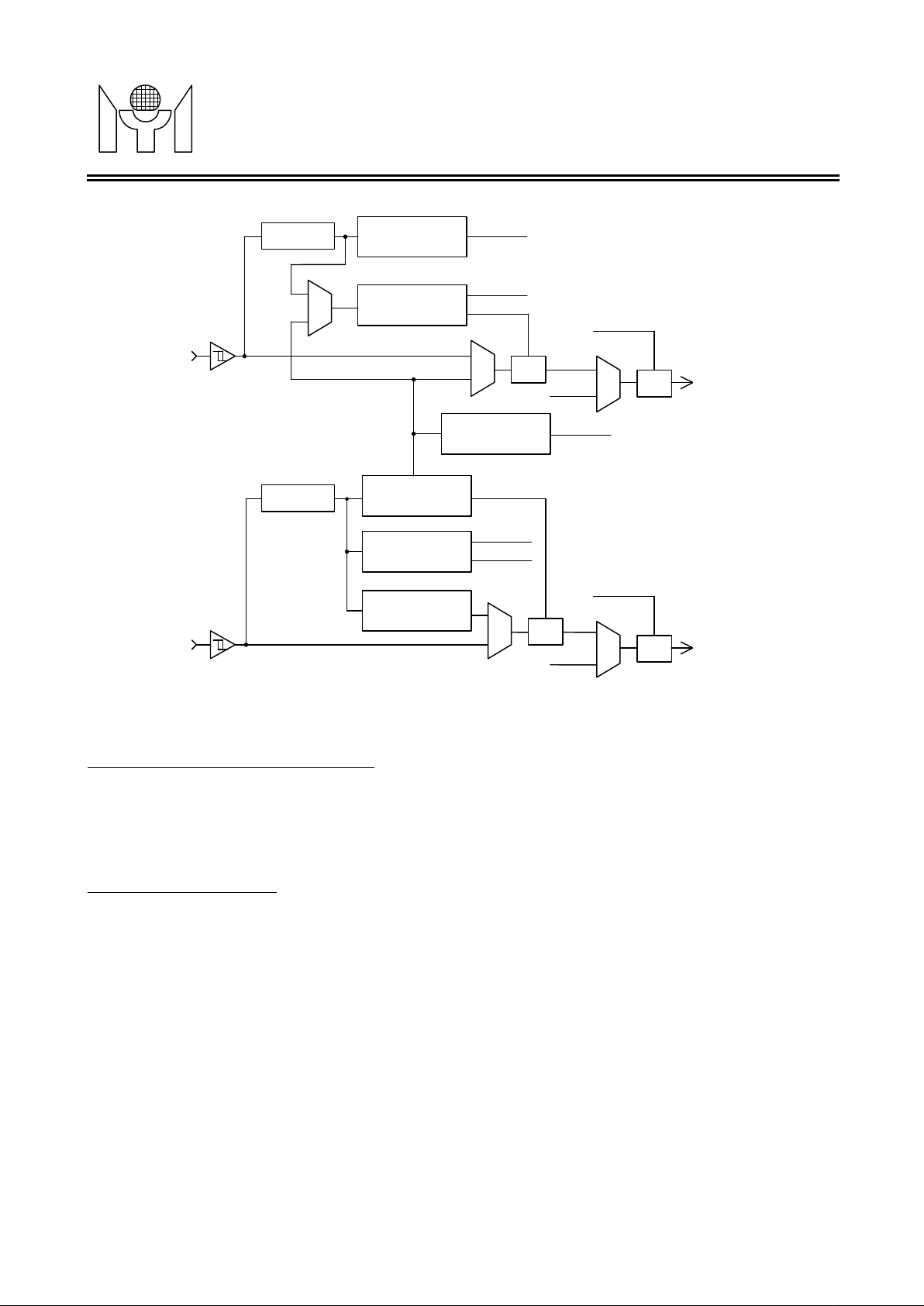
VSYNC/CVSYNC is present or continuously updated when VSYNC/CVS YNC is non-present. The 12 bits
Hself
Hpol
CVpre
Vbpl
VSYNC
Vpre
Vfreq
Vpol
VBLANK
Vself
HSYNC
CVSYNC
Hpre
Hfreq
Hbpl
HBLANK
XOR
MTV212M64
TECHNOLOGY
Digital Filter
Digital Filter
Present
Check
Polarity Check &
Freq. Count
Polarity Check &
Sync Seperator
Present Check &
Freq. Count
(Rev. 1.2)
XOR
XOR
Present
Check
Composite
Pulse Insert
XOR
H/V SYNC Processor Block Diagram
6.1 Composite SYNC separation/insertion
The MTV212M continuously monitors the input HSYNC, if the vertical SYNC pulse can be extracted from the
input, a CVpre flag is set and user can select the extracted "CVSYNC" for the source of polarity check,
frequency count, and VBLANK output. The CVSYNC will have 8us delay compared to the original signal.
The MTV212M can also insert pulse to HBLANK output during com posite VSYNC’s active time. The insert
pulse’s width is 1/8 HSYNC period and the insertion frequency can adapt to original HSYNC.
MTV212M can discriminate HSYNC/VSYNC frequency and saves the information in XFRs. The 14 bits
Hcounter counts the time of 64xHSYNC period, then load the result into the HCNTH/HCNTL latch. The
output value will be [(128000000/H-Freq) - 1], updated once per VSYNC/CVSYNC period when
Vcounter counts the time between two VSYNC pulses, then load the result into the VCNTH/VCNTL latch.
The output value will be (62500/V-Freq), updated every VSYNC/CVSYNC perio d. An extra overflow bit
indicates the condition of H/V counter overflow. The VFchg/HFchg interrupt is set when VCNT/HCNT value
changes or overflow. Table 4.2.1 and table 4.2.2 shows the HCNT/VCNT value under the operations of
12MHz.
Revision 1.2 - 9 - 2000/07/04
Page 10

MYSON
CVpre flag interrupt may be disabled when S/W disable the composite function.
6.4 H/V Polarity Detect
The polarity functions detect the input HSYNC/VSYNC high and low pulse duty cycle. If the high pulse
duration is longer than that of low pulse, the negative polarity is asserted; otherwise, positi ve polarity is
6.5 Output HBLANK/VBLANK Control and Polarity Adjust
MTV212M64
6.2.1 H-Freq Table
H-Freq(KHZ)
1
2
3
4
5
6
7
8
9
10
11
12
6.2.2 V-Freq Table
1
2
3
4
5
6
31.5
37.5
43.3
46.9
53.7
60.0
68.7
75.0
80.0
85.9
93.8
106.3
V-Freq(Hz)
TECHNOLOGY
Outpu t Value (14 bit s )
12MHz OSC (hex / dec)
0FDEh / 4062
0D54h / 3412
0B8Bh / 2955
0AA8h / 2728
094Fh / 2383
0854h / 2132
0746h / 1862
06AAh / 1706
063Fh / 1599
05D1h / 1489
0554h / 1364
04B3h / 1203
Outpu t value (12bits)
12MHz OSC (hex / dec)
56
60
70
72
75
85
45Ch / 1116
411h / 1041
37Ch / 892
364h / 868
341h / 833
2DFh / 735
(Rev. 1.2)
6.3 H/V Present Check
The Hpresent function checks the input HSYNC pulse, Hpre flag is set when HSYNC is over 10KHz or
cleared when HSYNC is under 10Hz. The Vpresent function checks the input VSYNC pulse, the Vpre flag is
set when VSYNC is over 40Hz or cleared when VSYNC is under 10Hz. The HPRchg interrupt is set when
the Hpre value changes. The VPRchg interrupt is set when the Vpre/CVpre value change. However, the
asserted. The HPLchg interrupt is set when the Hpol value changes. The VPLchg interrupt is set when the
Vpol value changes.
The HBLANK is the mux output of HSYNC, composite Hpulse and self-test horizontal pattern. The VBLANK
is the mux output of VSYNC, CVSYNC and self-test vertical pattern. The mux selection and output polarity
are S/W controllable. The VBLANK output is cut off when VSYNC frequency is over 200Hz. The
HBLANK/VBLANK shares the output pin with P4.1/ P4.0.
6.6 Self Test Pattern Generator
This generator can generate 4 display patterns for testing purpose, which are positive cross-hatch, negative
cross-hatch, full white, and full black (showed as following figure). The HBLANK output frequency of the
pattern can be chosen to 63.5KHz, 47.6KHz and 31.75KHz. The VBLANK output f requency of the pattern is
60Hz. It is originally designed to support monitor manufacturer to do burn-in test, or offer end-user a
reference to check the monitor. The generator's output STOUT shares the output pin with P4.2.
Revision 1.2 - 10 - 2000/07/04
Page 11

MYSON
MTV212M64
TECHNOLOGY
Display Region
Positive cross-hatch Negative cross-hatch
(Rev. 1.2)
Full white Full black
Revision 1.2 - 11 - 2000/07/04
Page 12

MYSON
* 8 x 8 blocks of cross hatch pattern in display region.
width and polarity is S/W controllable.
EVsync
The status of polarity, present and static level for HSYNC and VSYNC.
HSYNC input is positive polarity.
VSYNC (CVSYNC) is negative polarity.
MTV212M64
TECHNOLOGY
MTV212M Self-Test pattern timing
63.5KHz, 60Hz 47.6KHz, 60Hz 31.7KHz, 60Hz
Absolute time H dots Absolute time H dots Absolute time H dots
Hor. Total time (A) 15.75us 1280 21.0us 1024 31.5us 640
Hor. Active time (D) 12.05us 979.3 16.07us 783.2 24.05us 488.6
Hor. F. P. (E) 0.2us 16.25 0.28us 12 0.45us 9
SYNC pulse width (B) 1.5us 122 2us 90 3us 61
Hor. B. P. (C) 2us 162.54 2.67us 110 4us 81.27
Absolute time V lines Absolute time V lines Absolute time V lines
Vert. Total time (O) 16.663ms 1024 16.663ms 768 16.663ms 480
Vert. Active time (R) 15.655ms 962 15.655ms 721.5 15.655ms 451
Vert. F. P. (S) 0.063ms 3.87 0.063ms 2.9 0.063ms 1.82
SYNC pulse width (P) 0.063ms 3.87 0.063ms 2.9 0.063ms 1.82
Vert. B. P. (Q) 0.882ms 54.2 0.882ms 40.5 0.882ms 25.4
6.7 HSYNC Clamp Pulse Output
The HCLAMP output is active by setting “HCLPE” control bit. The HCLAMP’s leading edge position, pulse
(Rev. 1.2)
6.8 VSYNC Interrupt
The MTV212M check the VSYNC input pulse and generate an interrupt at its leading edge. The VSYNC flag
is set each time when MTV212M detects a VSYNC pulse. The flag is cleared by S/W writing a "0".
6.9 H/V SYNC Processor Register
Reg name addr bit7 bit6 bit5 bit4 bit3 bit 2 bit1 bit0
HVSTUS
HCNTH
HCNTL
VCNTH
VCNTL
HVCTR0
HVCTR2
HVCTR3
INTFLG
INTEN
HVSTUS (r) :
CVpre = 1 → The extracted CVSYNC is present.
H
pol
V
pol
H
pre
V
pre
H
off*
40h (r) CVpre Hpol Vpol Hpre Vpre Hoff Voff
41h (r) Hovf HF13 HF12 HF11 HF10 HF9 HF8
42h (r) HF7 HF6 HF5 HF4 HF3 HF2 HF1 HF0
43h (r) Vovf VF11 VF10 VF9 VF8
44h (r) VF7 VF6 VF5 VF4 VF3 VF2 VF1 VF0
40h (w) C1 C0 NoHins HBpl VBpl
42h (w) Selft STF1 STF0 Rt1 Rt0 STE
43h (w) CLPEG CLPPO CLPW2 CLPW1 CLPW0
48h (r/w) HPRchg VPRchg HPLchg VPLchg HFchg VFchg Vsync
49h (w) EHPR EVPR EHPL EVPL EHF EVF
= 0 → The extracted CVSYNC is not present.
= 1 →
= 0 → HSYNC input is negative polarity.
= 1 → VSYNC (CVSYNC) is positive polarity.
= 0 →
= 1 → HSYNC input is present.
= 0 → HSYNC input is not present.
= 1 → VSYNC input is present.
= 0 → VSYNC input is not present.
= 1 → HSYNC input's off level is high.
Revision 1.2 - 12 - 2000/07/04
Page 13

MYSON
Freq counter is overflow, this bit is clear by H/W when condition removed.
Freq counter's low byte.
positive polarity HBLANK output.
positive polarity VBLANK output.
Positive polarity clamp pulse output.
Negative polarity clamp pulse output.
: CLPW0 : Pulse width of clamp pulse is
:CLPW0) + 1] x 0.167
enable bit is set, the 8051 core's INT1 source will be driven by a zero level. Soft ware MUST
MTV212M64
TECHNOLOGY
= 0 → HSYNC input's off level is low.
V
*H
HCNTH (r) : H-Freq counter's high bits.
Hovf = 1 → HHF13 - HF8 : 6 high bits of H-Freq counter.
HCNTL (r) : H-Freq counter's low byte.
VCNTH (r) : V-Freq counter's high bits.
Vovf = 1 → V-Freq counter is overflow, this bit is clear by H/W when condition removed.
VF11 - 8 : 4 high bits of V-Freq counter.
VCNTL (r) : V-
HVCTR0 (w) : H/V SYNC processor control register 0.
C1, C0 = 1,1 → Select CVSYNC as the polar ity, freq and VBLANK source.
NoHins = 1 → HBLANK has no insert pulse in composite mode.
HB
VB
= 1 → VSYNC input's off level is high.
off*
= 0 → VSYNC input's off level is low.
and V
off
pl
pl
are valid when H
off
= 1,0 → Select VSYNC as the polarity, freq and VBLANK source.
= 0,0 → Disable composite function.
= 0,1 → H/W auto switch to CVSYNC when CVpre=1 and VSpre=0.
= 0 → HBLANK has insert pulse in composite mode.
= 1 → negative polarit y HBLANK output.
= 0 →
= 1 → negative polarit y VBLANK output.
= 0 →
pre=0
or V
pre=0.
(Rev. 1.2)
HVCTR2 (w) : Self-test pattern generator control.
S
elft
STF1,STF0 = 1,1 → 63.5KHz(horizontal) output selected.
Rt1, Rt0= 0,0 → positive cross-hatch pattern output.
STE = 1 → enable STOUT output.
HVCTR3 (w) : HSYNC clamp pulse control register.
CLPEG = 1 → Clamp pulse follows HSYNC leading edge.
CLPPO = 1 →
CLPW2
INTFLG (w) : Interrupt flag. An interrupt event will set its individual flag, and, if the corresponding interrupt
clear this register while serve the interrupt routine.
= 1 → enable generator.
= 0 → disable generator.
= 1,0 → 47.6KHz(horizontal) output selected.
= 0,0 → 31.75KHz(horizontal) output selected.
= 0,1 → negative cross-hatch pattern output.
= 1,0 → full white pattern output.
= 1,1 → full black pattern output.
= 0 → disable STOUT output.
= 0 → Clamp pulse follows HSYNC trailing edge.
= 0 →
[(CLPW2
µs for 12MHz X’tal selection.
Revision 1.2 - 13 - 2000/07/04
Page 14

MYSON
Clear HSYNC polarity change flag.
Clear VSYNC polarity change flag.
Indicates a HSYNC polarity change.
Enable VSYNC polarity change interrupt.
DbufI interrupt is automatically cleared when Software writes a new data byte to DBUF. The
Under such condition, the HSDA and HSCL are directly bypassed to ISDA and ISCL pins. The other way to
MTV212M64
TECHNOLOGY
HPRchg= 1 → No action.
= 0 → Clear HSYNC presence change flag.
VPRchg= 1 → No action.
= 0 → Clear VSYNC presence change flag.
HPLchg= 1 → No action.
= 0 →
VPLchg= 1 → No action.
HFchg = 1 → No action.
VFchg = 1 → No action.
Vsync = 1 → No action.
INTFLG (r) : Interrupt flag.
HPRchg= 1 → Indicates a HSYNC presence change.
VPRchg= 1 → Indicates a VSYNC presence change.
HPLchg= 1 →
VPLchg= 1 → Indicates a VSYNC polarity change.
HFchg = 1 → Indicates a HSYNC frequency change or counter overflow.
VFchg = 1 → Indicates a VSYNC frequency change or counter overflow.
Vsync = 1 → Indicates a VSYNC interrupt.
= 0 →
= 0 → Clear HSYNC frequency change flag.
= 0 → Clear VSYNC frequency change flag.
= 0 → Clear VSYNC interrupt flag.
(Rev. 1.2)
INTEN (w) : Interrupt enable.
EHPR = 1 → Enable HSYNC presence change interrupt.
EVPR = 1 → Enable VSYNC presence change interrupt.
EHPL = 1 → Enable HS YNC polarity change interrupt.
EVPL = 1 →
EHF = 1 → Enable HSYNC frequency change / counter overflow interrupt.
EVF = 1 → Enable VSYNC frequency change / counter overflow interrupt.
EVsync = 1 → Enable VSYNC interrupt.
7. DDC & IIC Int er face
7.1 DDC1 Mode
The MTV212M enters DDC1 mode after Reset. In this mode, VSYNC is used as data clock. The HSCL pin
should remain at high. The data output to the HSDA pin is taken from a shift register in MTV212M. The shift
register fetch data byte from the DDC1 data buffer (DBUF) then send it in 9 bits packet formats which
includes a null bit (=1) as packet separator. The DBUF set the DbufI interrupt flag when the shift register
read out the data byte from DBUF. Software needs to write EDID data to DBUF as soon as the DbufI is set.
The
interrupt can be mask or enable by EDbufI control bit.
7.2 DDC2B Mode
The MTV212M switches to DDC2B mode when it detects a high to low transition on th e HSCL pin. Once
MTV212M enters DDC2B mode, S/W can set IICpass control bit to allow HOST access EEPROM directly.
DbufI
perform DDC2 function is to clear IICpass and config the Slave A IIC block to act as EEPROM behavior. The
Slave A block's slave address can be chosen by S/W as 5-bits, 6-bits or 7-bits. For example, if S/W choose
5-bits slave address as 10100b, the slave IIC block A will respond to slave address 10100xx b and save the 2
LSB "xx" in XFR. This feature enables MTV212M to meet PC99 requirement.
The MTV212M will return to DDC1 mode if HSCL is kept high for 128 VSYNC clock period. However, it will
Revision 1.2 - 14 - 2000/07/04
Page 15

MYSON
RCABUF/RCBBUF register when a data byte is received. The first byte loaded is word address (slave
the RCABUF/RCBBUF is loaded. If S/W can't read out the RCABUF/RCBBUF in time, the next byte in shift
every time when shift register reads out the data from TX ABUF/TXBBUF.
SlvBMI is cleared by writing "0" to corresponding bit in INTFLG register.
The TXAI/TXBI is cleared by writing TXABUF/TXBBUF. If the control
The master mode IIC block can be connected to the ISDA /ISCL pins or the HSDA/HSCL pins, select by
Msel control bit. Its speed can be selected to 50KHz-400KHz by S/W setting the MIICF1/MIICF0 control bit.
and the display information share the common EEPROM, precaution m ust be taken to avoid bus conflicting
while Msel=0. In DDC1 mode or IICpass=0, the ISCL/ISDA is controlled by MTV212M only. In DDC2 mode
IICpass flag is set, the host may access the EEPROM directl y. Software can test the HSCL condition by
1. Write MBUF the Slave Address.
3. After the MTV212M transmit this byte, a
1. Write MBUF the Slave Address.
3. After the MTV212M transmit this byte, a
MTV212M64
TECHNOLOGY
lock in DDC2B mode if a valid IIC address (1010xxxb) has been detected on HSCL/HSDA bus. The DDC2
flag reflects the current DDC status, S/W may clear it by writing a "0" to it.
7.3 Slave Mode IIC function Block
The slave mode IIC block is connected to HSDA and HSCL pins. This block can receive/transmit data using
IIC protocol. There are 2 slave addresses MTV212M can respond to. S/W may write the
SLVAADR/SLVBADR register to determine the slave addresses. The SlaveA address can be configured to
5-bits, 6-bits or 7-bits by S/W setting the SlvAbs1 and SlvAbs0 control bits.
In receive mode, the block first detects IIC slave address match condition then issues a SlvAMI/SlvBMI
interrupt. If the matched address is slave A, MTV212M will save the matched address's 2 LSB bits to
SlvAlsb1 and SlvAlsb0 register. The data from HSDA is shifted into shift register then written to
address is dropped). This block also generates a RCAI/RCBI (receive buff er full interrupt) every time when
register will not be written to RCABUF/RCBBUF and the slave block return NACK to the master. This feature
guarantees the data integrity of communication. The WadrA/WadrB flag can tell S/W that if the data in
RCABUF/RCBBUF is a word address.
In transmit mode, the block first detects IIC slave address match condition then issues a SlvAMI/SlvBMI
interrupt. In the mean time, the SlvAlsb1/SlvAlsb0 is also updated if the matched address is sla ve A, and the
data pre-stored in the TXABUF/TXBBUF is loaded into shift register, result in TXABUF/T XBBUF empty and
generates a TXAI/TXBI (transmit buffer empty interrupt). S/W should write the TXABUF/TXBBUF a new byte
for next transfer before shift register empty. Fail to do this will cause data corrupt. The TXAI/TXBI occurs
(Rev. 1.2)
The SlvAMI/
cleared by reading RCABUF/RCBBUF.
bit ENSCL is set, the block will hold HSCL low until the RCAI/RCBI/TXAI/TXBI is cleared.
*Please see the attachments about "Slave IIC Block Timing".
7.4 Master Mode IIC Function Block
The software program can access the external IIC device through this interface. Since th e ED ID/VDIF data
and
reading the Hbusy flag, which is set in case of HSCL=0, and keeps high for 100uS after t he HSCL's rising
edge. S/W can launch the master IIC transmit/receive by clearing the P bit. Once P=0, MTV212M will hold
HSCL low to isolate the host's access to EEPROM. A summary of master IIC access is illustrated as follows.
7.4.1. To write IIC Device
2. Set S bit to Start.
4. Program can write MBUF to transfer next byte or set P bit to stop.
* Please see the attachments about "Master IIC Transmit Timing".
7.4.2. To read IIC Device
MbufI interrupt will be triggered.
The RCAI/RCBI is
2. Set S bit to Start.
4. Set or reset the MAckO flag according to the IIC protocol.
5. Read out MBUF the useless byte to continue the data transfer.
6. After the MTV212M receives a new byte, the MbufI interrupt is triggered again.
7. Read MBUF also trigger the next receive operation, but set P bit before read can terminate the operation.
Revision 1.2 - 15 - 2000/07/04
MbufI interrupt will be triggered.
Page 16

MYSON
WadrB
WadrA
SLVAADR
SLVBADR
In master receive mode, NACK is returned by MTV212M.
In master receive mode, ACK is returned by MTV212M.
enable bit is set, the 8051 INT1 source will be driven by a zero level. Software MUST clear
MTV212M64
TECHNOLOGY
* Please see the attachments about "Master IIC Receive Timing".
Reg name addr bit7 bit6 bit5 bit4 bit3 bit 2 bit1 bit0
IICCTR
IICSTUS
IICSTUS
INTFLG
INTFLG
INTEN
MBUF
RCABUF
TXABUF
RCBBUF
TXBBUF
DBUF
IICCTR (r/w) : IIC interface control register.
DDC2 = 1 → MTV212M is in DDC2 mode, write "0" can clear it.
MAckO = 1 →
S, P = ↑, 0 → Start condition when Master IIC is not during transfer.
* A write/read MBUF operation can be recognized only after 10us of the MbufI flag's rising edge.
00h (r/w) DDC2 MAckO P S
01h (r)
02h (r) MAckIn Hifreq Hbusy
03h (r) TXBI RCBI SlvBMI TXAI RCAI SlvAMI DbufI MbufI
03h (w) SlvBMI SlvAMI MbufI
04h (w) ETXBI ERCBI ESlvBMI ETXAI ERCAI ESlvAMI EDbufI EMbufI
05h (r/w) Master IIC receive/transmit data buffer
06h (r) Slave A IIC receive buffer
06h (w) Slave A IIC transmit buffer
07h (w) ENSlvA Slave A IIC address
08h (r) Slave B IIC receive buffer
08h (w) Slave B IIC transmit buffer
09h (w) ENSlvB Slave B IIC address
0Ah (w) DDC1 transmit data buffer
= 0 → MTV212M is in DDC1 mode.
= 0 →
= X, ↑ → Stop condition when Master IIC is not during transfer.
= 1, X → Will resume transfer after a read/write MBUF operation.
= X, 0 → Force HSCL low and occupy the master IIC bus.
SlvRWB SAckIn SLVS SlvAlsb1 SlvAlsb0
(Rev. 1.2)
IICSTUS (r) : IIC interface status register.
WadrB = 1 → The data in RCBBUF is word address.
WadrA = 1 → The data in RCABUF is word address.
SlvRWB = 1 → Current transfer is slave transmit
= 0 → Current transfer is slave receive
SAckIn = 1 → The external IIC host respond NACK.
SLVS = 1 → The slave block has detected a START, cleared when STOP detected.
SlvAlsb1,SlvAlsb0 : The 2 LSB which host send to Slave A block.
MAckIn = 1 → Master IIC bus error, no ACK received from the slave IIC device.
= 0 → ACK received from the slave IIC device.
Hifreq = 1 → MTV212M has detected a higher than 200Hz clock on the VSYNC pin.
Hbusy = 1 → Host drives the HSCL pin to low.
INTFLG (w) : Interrupt flag. A interrupt event will set its individual flag, and, if the corresponding interrupt
this register while serve the interrupt routine.
SlvBMI = 1 → No action.
= 0 → Clear SlvBMI flag.
SlvAMI = 1 → No action.
= 0 → Clear SlvAMI flag.
MbufI = 1 → No action.
= 0 → Clear Master IIC bus interrupt flag (MbufI).
INTFLG (r) : Interrupt flag.
Revision 1.2 - 16 - 2000/07/04
Page 17

MYSON
When the voltage level of power supply is below 4.0V for a specific time, the LVR will generate a
Xtal cycle to guarantee the
WDT(2:0). The timer
MTV212M64
TECHNOLOGY
TXBI = 1 → Indicates the T XBBUF need a new data byte, clear by writing TXBBUF.
RCBI = 1 → Indicates the RCBBUF has received a new data byte, clear by reading RCBBUF.
SlvBMI = 1 → Indicates the slave IIC address B match condition.
TXAI = 1 → Indicates the T XABUF need a new data byte, clear by writing TXABUF.
RCAI = 1 → Indicates the RCABUF has received a new data byte, clear by reading RCABUF.
SlvAMI = 1 → Indicates the slave IIC address A match condition.
DbufI = 1 → Indicates the DDC1 data buffer need a new data byte, clear by writing DBUF.
MbufI = 1 → Indicates a byte is sent/received to/from the master IIC bus.
INTEN (w) : Interrupt enable.
ETXBI = 1 → Enable TXBBUF interrupt.
ERCBI = 1 → Enable RCBBUF interrupt.
ESlvBMI = 1 → Enable slave address B match interrupt.
ETXAI = 1 → Enable TXABUF interrupt.
ERCAI = 1 → Enable RCABUF interrupt.
ESlvAMI = 1 → Enable slave address A match interrupt.
EDbufI = 1 → Enable DDC1 data buffer interrupt.
EMbufI = 1 → Enable Master IIC bus interrupt.
Mbuf (w) : Master IIC data shift register, after START and before STOP condition, write this register will
resume MTV212M's transmission to the IIC bus.
(Rev. 1.2)
Mbuf (r) : Master IIC data shift register, after START and before STOP condition, read this register will
resume MTV212M's receiving from the IIC bus.
RCABUF (r) : Slave IIC block A receive data buffer.
TXABUF (w) : Slave IIC block A transmit data buffer.
SLVAADR (w) :Slave IIC block A's enable and address.
ENslvA = 1 → Enable slave IIC block A.
= 0 → Disable slave IIC block A.
bit6-0 : Slave IIC address A to which the slave block should respond.
RCBBUF (r) : Slave IIC block B receive data buffer.
TXBBUF (w) : Slave IIC block B transmit data buffer.
SLVBADR (w) :Slave IIC block B's enable and address.
ENslvB = 1 → Enable slave IIC block B.
= 0 → Disable slave IIC block B.
bit6-0 : Slave IIC address B to which the slave block should respond.
8. Low Pow er Reset (LVR) & Watchdog Tim er
chip reset
signal. After the power supply is above 4.0V, LVR maintain in reset state for 144
chip exit reset condition with a stable X'tal oscillation.
The WatchDog Timer automatically generates a device reset when it is overflow. The interval of overflow is
0.25 sec x N, where N is a number from 1 to 8, and can be programmed via register
function is disabled after power on reset, user can activate this function by setting WEN, and clear the timer
by set WCLR.
Revision 1.2 - 17 - 2000/07/04
Page 18

MYSON
9. A/D con v ert er
WCLR
WDT2
WDT1
WDT0
Watchdog Timer control register.
Volt Regulator. The SIE block performs most of the USB interface function with only minimum support from
4. TOKEN type identification
S/W handles the following tasks:
MTV212M64
TECHNOLOGY
The MTV212M is equipped with four 6-bit A/D converters, S/W can select the current convert channel by
setting the SADC1/SADC0 bit. The refresh rate for the ADC is OSC freq./12288. The ADC compare the input
pin voltage with internal VDD*N/64 voltage (where N = 0 - 63). The ADC output value is N when pin voltage
is greater than VDD*N/64 and smaller than VDD*(N+1)/64.
Reg name addr bit7 bit6 bit5 bit4 bit3 bit 2 bit1 bit0
ADC
ADC
WDT
WDT (w) :
WEN = 1 → Enable WatchDog Timer.
WCLR = 1 → Clear WatchDog Timer.
WDT2: WDT0 = 0 → overflow interval = 8 x 0.25 sec.
10h (w) ENADC SADC3 SADC2 SADC1 SADC0
10h (r) ADC convert Result
18h (w) WEN
= 1 → overflow interval = 1 x 0.25 sec.
= 2 → overflow interval = 2 x 0.25 sec.
= 3 → overflow interval = 3 x 0.25 sec.
= 4 → overflow interval = 4 x 0.25 sec.
= 5 → overflow interval = 5 x 0.25 sec.
= 6 → overflow interval = 6 x 0.25 sec.
= 7 → overflow interval = 7 x 0.25 sec.
(Rev. 1.2)
ADC (w) : ADC control.
ENADC = 1 → Enable ADC.
SADC0 = 1 → Select ADC0 pin input.
SADC1 = 1 → Select ADC1 pin input.
SADC2 = 1 → Select ADC2 pin input.
SADC3 = 1 → Select ADC3 pin input.
ADC (r) : ADC convert result.
10. USB Engine
The USB engine includes the Serial Interface Engine (SIE), the low-speed USB I/O transc eiver and the 3.3
S/W. Two endpoints are supported. Endpoint 0 is used to receive and transmit control (including SETUP)
packets while Endpoint 1 is only used to transmit data packets.
The USB SIE handles the following USB bus activity independently:
1. Bitstuffing/unstuffing
2. CRC generation/checking
3. ACK/NAK
5. Address checking
1. Coordinate enumeration by responding to SETUP packets
2. Fill and empty the FIFOs
3. Suspend/Resume coordination
4. Verify and select DATA toggle values
10.1 USB Device Address
The USBADR register stores the device address. This register is reset to all 0 after chip reset or USB bus
Revision 1.2 - 18 - 2000/07/04
Page 19

MYSON
Endpoint 0 transmit FIFO (TX0FIFO) to the USB bus if the Endpoint 0 transmit ready flag (TX0rdy) is set and
(EP1Cfgd) is set. After detecting a valid Endpoint 1 IN token, MTV212M automatically transmit the data pre-
X'tal is stop, but CPU can be waken-up by the trigger of enabled INT 1's source. In
MTV212M64
TECHNOLOGY
reset. S/W must write this register a valid value after the USB enumeration process.
10.2 Endpoint 0 receive
After receiving a packet and placing the data into the Endpoint 0 receive FIFO (RC0FIFO), MTV212M
updates the Endpoint 0 status register (EP0STUS) to record the receive status and then g enerates an
Endpoint 0 receive interrupt (RC0I). S/W can read the EP0STUS register for the recent tra nsfer information,
which includes the data byte count (RC0cnt), data direction (EP0dir), SETUP token flag (EP0set) and data
valid flag (RC0err). The received data is always stored into RC0FIFO and the RC0cnt is always updated for
DATA packets following SETUP tokens. The data following an OUT tok en is written into th e RC0FIFO, and
the RC0cnt is updated unless Endpoint 0 STALL (EP0stall) or Endpoint 0 receive NAK (RC0nak) is set. The
RC0I interrupt will happen in case where the RC0cnt/RC0FIFO is updated.
10.3 Endpoint 0 transmit
After detecting a valid Endpoint 0 IN token, MTV212M automaticall y transmit the data pre-stored in the
the EP0stall is cleared. The number of byte to be transmitted is base on the Endpoint 0 tra nsmit byte count
register (TX0cnt). The DATA0/1 token to be transmitted is base on the Endpoint 0 transmit toggle control bit
(TX0tgl). After the TX0FIFO is updated, TX0rdy should be set to 1. This enables the MTV212M to respond to
an Endpoint 0 IN packet. TX0rdy is cleared and an Endpoint 0 transmit interrupt (TX0I) is generated once the
USB host acknowledges the data transmission. The interrupt service routine can check TX0rdy to confirm
that the data transfer was successful.
(Rev. 1.2)
10.4 Endpoint 1 transmit
Endpoint 1 is capable of transmit only. This endpoint is enable when the Endpoint1 configured control bit
stored in the Endpoint 1 transmit FIFO (TX1FIFO) to the USB bus if the Endpoint 1 transmit ready flag
(TX1rdy) is set and the EP1stall is cleared. The number of byte to be transmitted is base on the Endpoint 1
transmit byte count register (TX1cnt). The DATA0/1 token to be transmitted is base on the Endpoint 1
transmit toggle control bit (TX1tgl). After the TX1FIFO is updated, TX1rdy should be set to 1. This enables
the MTV212M to respond to an Endpoint 1 IN packet. TX 1rdy is cleared and an Endpoint 1 transmit interrupt
(TX1I) is generated once the USB host acknowledges the data transmission. The interrupt service routine
can check TX0rdy to confirm that the data transfer was successful.
10.5 USB Control and Status
Other USB control bits include the USB enable (ENUSB), SUSPEND (Susp), RESUME (RsmO), Control
Read (CtrRD), and corresponding interrupt enable bits. The CtrRD should be set when program detects the
current transfer is an Endpoint0 Control Read Transfer. Once this bit is set, the MTV212M will stall an
Endpoint0 OUT packet with DATA toggle 0 or byte count other than 0. Other US B status flag includes the
USB reset interrupt (USBrstI), RESUME interrupt (RsmI), and USB bus active flag (USBactv). The USBactv
flag is set once the MTV212M detect the USB bus activity. S/W should read and clear it every 3 ms to
identify the suspend condition. Writing a "1" to the USBactv flag will not change its value.
10.6 Suspend and Resume
Once the Suspend condition is asserted, S/W can set the Susp bit to stop the USBSIE's clock. In the mean
time, the 3.3V Regulator is operating in low power mode. S/W can further save the device power by force the
8051 CPU core into the Power Down or Idle mode by setting the PCON register in SFR area. In the Idel
mode, the X'tal keeps oscillating and CPU can be waken-up by the trigger of any enabled interrupt. In the
Power Down mode, the
short, S/W can keep the RsmI alive before enter the suspend mode.
Reg name addr bit7 bit6 bit5 bit4 bit3 bit 2 bit1 bit0
USBADR
INTFLG
INTEN
EP0STUS
Revision 1.2 - 19 - 2000/07/04
60h (r/w) ENUSB USBadr
61h (r/w) USBrstI RC0I T X1I TX0I RsmI
62h (w) EUrstI ERC0I ETX1I ETX0I ERsmI
63h (r) RC0tgl RC0err EP0dir EP0set RC0cnt
Page 20

MYSON
Endpoint 0 receive FIFO 1st byte
Endpoint 0 receive FIFO 2nd byte
Endpoint 0 receive FIFO 3rd byte
Endpoint 0 transmit FIFO 3rd byte
Endpoint 0 transmit FIFO 4th byte
Endpoint 0 transmit FIFO 5th byte
Endpoint 0 transmit FIFO 6th byte
Endpoint 0 transmit FIFO 7th byte
Endpoint 0 transmit FIFO 8th byte
Endpoint 1 transmit FIFO 3rd byte
Endpoint 1 transmit FIFO 4th byte
Endpoint 1 transmit FIFO 5th byte
Endpoint 1 transmit FIFO 6th byte
Endpoint 1 transmit FIFO 7th byte
Endpoint 1 transmit FIFO 8th byte
enable bit is set, the 8051 INT1 source will be driven by a zero level. Software MUST clear
MTV212M64
TECHNOLOGY
USBCTR
TX0CTR
TX0CTR
TX1CTR
TX1CTR
RC0FIFO
RC0FIFO
RC0FIFO
RC0FIFO
RC0FIFO
RC0FIFO
RC0FIFO
RC0FIFO
TX0FIFO
TX0FIFO
TX0FIFO
TX0FIFO
TX0FIFO
TX0FIFO
TX0FIFO
TX0FIFO
TX1FIFO
TX1FIFO
TX1FIFO
TX1FIFO
TX1FIFO
TX1FIFO
TX1FIFO
TX1FIFO
USBADR (r/w) : USB device address and enable.
ENUSB = 1 → Enable USB function, clear while chip reset.
USBadr : USB device address, clear while chip reset or USB bus reset.
64h (r/w) Susp RsmO EP1cfgd RC0nak CtrRD USBactv
65h (w) TX0rdy TX0tgl EP0stall TX0cnt
65h (r) TX0rdy TX0tgl EP 0stall
66h (w) TX1rdy TX1tgl EP1stall TX1cnt
66h (r) TX1rdy TX1tgl EP 1stall
68h (r)
69h (r)
6Ah (r)
6Bh (r) Endpoint 0 receive FIFO 4th byte
6Ch (r) Endpoint 0 receive FIFO 5th byte
6Dh (r) Endpoint 0 receive FIFO 6th byte
6Eh (r) Endpoint 0 receive FIFO 7th byte
6Fh (r) Endpoint 0 receive FIFO 8th byte
70h (w) Endpoint 0 transmit FIFO 1st byte
71h (w) Endpoint 0 transmit FIFO 2nd byte
72h (w)
73h (w)
74h (w)
75h (w)
76h (w)
77h (w)
78h (w) Endpoint 1 transmit FIFO 1st byte
79h (w) Endpoint 1 transmit FIFO 2nd byte
7Ah (w)
7Bh (w)
7Ch (w)
7Dh (w)
7Eh (w)
7Fh (w)
(Rev. 1.2)
INTFLG (w) : Interrupt flag. A interrupt event will set its individual flag, and, if the corresponding interrupt
this register while serve the interrupt routine.
USBrstI= 1 → No action.
= 0 → Clear USBrstI flag.
RC0I = 1 → No action.
= 0 → Clear RC0I flag.
TX1I = 1 → No action.
= 0 → Clear TX1I flag.
TX0I = 1 → No action.
= 0 → Clear TX0I flag.
RsmI = 1 → No action.
= 0 → Clear RsmI flag.
INTFLG (r) : Interrupt flag.
USBrstI= 1 → Indicates the USB bus reset condition.
RC0I = 1 → Endpoint 0 has completed a receive transfer and save the data in RC0FIFO.
TX1I = 1 → Endpoint 1 has completed a transmit transfer and empty TX1FIFO.
Revision 1.2 - 20 - 2000/07/04
Page 21

MYSON
Last transfer's receive byte count.
MTV212M detects USB bus activity, clear by S/W writing "0".
Endpoint 0 transmit byte count, write only.
Endpoint 1 transmit byte count, write only.
MTV212M64
TECHNOLOGY
TX0I = 1 → Endpoint 0 has completed a transmit transfer and empty TX0FIFO.
RsmI = 1 → Indicates the USB bus RESUME condition in suspend mode.
INTEN (w) : Interrupt enable.
EUrstI = 1 → Enable USBrstI interrupt.
ERC0I = 1 → Enable RC0I interrupt.
ETX1I = 1 → Enable TX1I interrupt.
ETX0I = 1 → Enable TX0I interrupt.
ERsmI = 1 → Enable RsmI interrupt.
EP0STUS (r) : Endpoint 0 status.
RC0tgl = 1 → Receive a DATA1 packet.
= 0 → Receive a DATA0 packet.
RC0err = 1 → Receive DATA packet error.
= 0 → Receive DATA packet good.
EP0dir = 1 → Last transfer is transmit direction (IN).
= 0 → Last transfer is receive direction (OUT, SETUP).
EP0set = 1 → Last transfer is a SETUP.
= 0 → Last transfer is not a SETUP.
RC0cnt :
(Rev. 1.2)
USBCTR (r/w) :USB control register.
Susp = 1 → S/W force USB interface into suspend mode.
RsmO = 1 → S/W force USB interface into send RESUME signal in suspend mode.
EP1cfgd = 1 → Endpoint 1 is configed.
RC0nak = 1 → Endpoint 0 will respond NAK to OUT token.
CtrRD = 1 → MTV212M will stall a invalid OUT token during Control Read transfer.
USBactv = 1 →
TX0CTR (r/w) : Endpoint 0 transmit control register.
TX0rdy = 1 → Enable the Endpoint 0 to respond to IN token.
TX0tgl = 1 → Endpoint 0 will transmit DATA1 packet.
EP0stall = 1 → Endpoint 0 will stall OUT/IN packet.
TX0cnt :
TX1CTR (r/w) : Endpoint 1 transmit control register.
TX1rdy = 1 → Enable the Endpoint 1 to respond to IN token.
TX1tgl = 1 → Endpoint 1 will transmit DATA1 packet.
EP1stall = 1 → Endpoint 1 will stall IN packet.
TX1cnt :
= 0 → Endpoint 0 will respond NAK to IN token.
This bit can be set or cleared by S/W, clear by H/W while Host acknowledge the transfer.
= 0 → Endpoint 0 will transmit DATA0 packet.
= 0 → Endpoint 1 will respond NAK to IN token.
This bit can be set or cleared by S/W, clear by H/W while Host acknowledge the transfer.
= 0 → Endpoint 1 will transmit DATA0 packet.
RC0FIFO (r) : Endpoint 0 receive FIFO registers.
TX0FIFO (w) : Endpoint 0 transmit FIFO registers.
TX1FIFO (w) : Endpoint 1 transmit FIFO registers.
Revision 1.2 - 21 - 2000/07/04
Page 22

MYSON
WadrB
WadrA
SLVAADR
SLVBADR
WCLR
WDT2
WDT1
WDT0
Pulse width of PWM DAC 0
Pulse width of PWM DAC 1
Pulse width of PWM DAC 2
Pulse width of PWM DAC 3
Pulse width of PWM DAC 4
Pulse width of PWM DAC 5
Pulse width of PWM DAC 6
Pulse width of PWM DAC 7
Pulse width of PWM DAC 8
Pulse width of PWM DAC 9
Pulse width of PWM DAC 10
Pulse width of PWM DAC 11
Pulse width of PWM DAC 12
Pulse width of PWM DAC 13
PWMF
EVsync
MTV212M64
TECHNOLOGY
(Rev. 1.2)
Memor y Map of XFR
Reg name addr bit7 bit6 bit5 bit4 bit3 bit 2 bit1 bit0
IICCTR
IICSTUS
IICSTUS
INTFLG
INTFLG
INTEN
MBUF
RCABUF
TXABUF
RCBBUF
TXBBUF
DBUF
ADC
ADC
WDT
DA0
DA1
DA2
DA3
DA4
DA5
DA6
DA7
DA8
DA9
DA10
DA11
DA12
DA13
PADMOD
PADMOD
PADMOD
OPTION
OPTION
XBANK
PORT4
PORT5
HVSTUS
HCNTH
HCNTL
VCNTH
VCNTL
HVCTR0
HVCTR2
HVCTR3
INTFLG
INTEN
00h (r/w) DDC2 MAckO P S
01h (r)
02h (r) MAckIn Hifreq Hbusy
03h (r) TXBI RCBI SlvBMI TXAI RCAI SlvAMI DbufI MbufI
03h (w) SlvBMI SlvAMI MbufI
04h (w) ETXBI ERCBI ESlvBMI ETXAI ERCAI ESlvAMI EDbufI EMbufI
05h (r/w) Master IIC receive/transmit data buffer
06h (r) Slave A IIC receive buffer
06h (w) Slave A IIC transmit buffer
07h (w) ENSlvA Slave A IIC address
08h (r) Slave B IIC receive buffer
08h (w) Slave B IIC transmit buffer
09h (w) ENSlvB Slave B IIC address
0Ah (w) DDC1 transmit data buffer
10h (w) ENADC SADC3 SADC2 SADC1 SADC0
10h (r) ADC convert Result
18h (w) WEN
20h (r/w)
21h (r/w)
22h (r/w)
23h (r/w)
24h (r/w)
25h (r/w)
26h (r/w)
27h (r/w)
28h (r/w)
29h (r/w)
2Ah (r/w)
2Bh (r/w)
2Ch (r/w)
2Dh (r/w)
30h (w) DA13E DA12E DA11E DA10E AD3E AD2E AD1E AD0E
31h (w) P56E P55E P54E P53E P52E P51E P50E
32h (w) HIICE IIICE HLFVE HLFHE HCLPE P42E P41E P40E
33h (w)
34h (w) SlvAbs1 SlvAbs0
35h (r/w) Xbnk2 Xbnk1 Xbnk0
38h (w) P42 P41 P40
39h (r/w) P56 P55 P54 P53 P52 P51 P50
40h (r) CVpre Hpol Vpol Hpre Vpre Hoff Voff
41h (r) Hovf HF13 HF12 HF11 HF10 HF9 HF8
42h (r) HF7 HF6 HF5 HF4 HF3 HF2 HF1 HF0
43h (r) Vovf VF11 VF10 VF9 VF8
44h (r) VF7 VF6 VF5 VF4 VF3 VF2 VF1 VF0
40h (w) C1 C0 NoHins HBpl VBpl
42h (w) Selft STF1 STF0 Rt1 Rt0 STE
43h (w) CLPEG CLPPO CLPW2 CLPW1 CLPW0
48h (r/w) HPRchg VPRchg HPLchg VPLchg HFchg VFchg Vsync
49h (w) EHPR EVPR EHPL EVPL EHF EVF
DIV253 FclkE IICpass ENSCL Msel MIICF1 MIICF0
SlvRWB SAckIn SLVS SlvAlsb1 SlvAlsb0
Revision 1.2 - 22 - 2000/07/04
Page 23

MYSON
Endpoint 0 receive FIFO 1st byte
Endpoint 0 receive FIFO 2nd byte
Endpoint 0 receive FIFO 3rd byte
Endpoint 0 transmit FIFO 3rd byte
Endpoint 0 transmit FIFO 4th byte
Endpoint 0 transmit FIFO 5th byte
Endpoint 0 transmit FIFO 6th byte
Endpoint 0 transmit FIFO 7th byte
Endpoint 0 transmit FIFO 8th byte
Endpoint 1 transmit FIFO 3rd byte
Endpoint 1 transmit FIFO 4th byte
Endpoint 1 transmit FIFO 5th byte
Endpoint 1 transmit FIFO 6th byte
Endpoint 1 transmit FIFO 7th byte
Endpoint 1 transmit FIFO 8th byte
MTV212M64
USBADR
INTFLG
INTEN
EP0STUS
USBCTR
TX0CTR
TX0CTR
TX1CTR
TX1CTR
RC0FIFO
RC0FIFO
RC0FIFO
RC0FIFO
RC0FIFO
RC0FIFO
RC0FIFO
RC0FIFO
TX0FIFO
TX0FIFO
TX0FIFO
TX0FIFO
TX0FIFO
TX0FIFO
TX0FIFO
TX0FIFO
TX1FIFO
TX1FIFO
TX1FIFO
TX1FIFO
TX1FIFO
TX1FIFO
TX1FIFO
TX1FIFO
TECHNOLOGY
60h (r/w) ENUSB USBadr
61h (r/w) USBrstI RC0I T X1I TX0I RsmI
62h (w) EUrstI ERC0I ETX1I ETX0I ERsmI
63h (r) RC0tgl RC0err EP0dir EP0set RC0cnt
64h (r/w) Susp RsmO EP1cfgd RC0nak CtrRD USBactv
65h (w) TX0rdy TX0tgl EP0stall TX0cnt
65h (r) TX0rdy TX0tgl EP 0stall
66h (w) TX1rdy TX1tgl EP1stall TX1cnt
66h (r) TX1rdy TX1tgl EP 1stall
68h (r)
69h (r)
6Ah (r)
6Bh (r) Endpoint 0 receive FIFO 4th byte
6Ch (r) Endpoint 0 receive FIFO 5th byte
6Dh (r) Endpoint 0 receive FIFO 6th byte
6Eh (r) Endpoint 0 receive FIFO 7th byte
6Fh (r) Endpoint 0 receive FIFO 8th byte
70h (w) Endpoint 0 transmit FIFO 1st byte
71h (w) Endpoint 0 transmit FIFO 2nd byte
72h (w)
73h (w)
74h (w)
75h (w)
76h (w)
77h (w)
78h (w) Endpoint 1 transmit FIFO 1st byte
79h (w) Endpoint 1 transmit FIFO 2nd byte
7Ah (w)
7Bh (w)
7Ch (w)
7Dh (w)
7Eh (w)
7Fh (w)
(Rev. 1.2)
Test Mode Conditi o n
In normal application, users should avoid the MTV212M entering its test/program mode, outlined as follow:
Test Mode A: RESET=1 & DA9=1 & DA8=0 & STO=0
Test Mode B: RESET's falling edge & DA9=1 & DA8=0 & STO=1
Program Mode: RESET=1 & DA9=0 & DA8=1
Revision 1.2 - 23 - 2000/07/04
Page 24

MYSON
ELECTRICAL PARA METERS
1. Absolu t e Maximum Rating s
Maximum Supply Voltage
2. Allowable Operating Condit io ns
Power Supply Current
4. AC Characterist ic s
PWM DAC Frequency
tVIPW
tVCPW
MTV212M64
TECHNOLOGY
at: Ta= 0 to 70 oC, VSS=0V
Name Symbol Range Unit
VDD -0.3 to +6.0 V
Maximum Input Voltage Vin -0.3 to VDD+0.3 V
Maximum Output Voltage Vout -0.3 to VDD+0.3 V
Maximum Operating Temperature Topg 0 to +70 o
Maximum Storage Temperature Tstg -25 to +125 o
at: Ta= 0 to 70 oC, VSS=0V
Name Symbol Min. Max. Unit
Supply Voltage VDD 4.5 5.5 V
Input "H" Voltage Vih1 0.4 x VDD VDD +0.3 V
Input "L" Voltage Vil1 -0.3 0.2 x VDD V
Operating Freq. Fopg - 15 MHz
(Rev. 1.2)
C
C
3. DC Characteri s t i c s
at: Ta=0 to 70 oC, VDD=5.0V, VSS=0V
Name Symbol Condition Min . Typ . Max. Unit
Output "H" Voltage, open drain pin Voh1 Ioh=0uA 4 V
Output "H" Voltage, 8051 I/O port pin Voh2 Ioh=-50uA 4 V
Output "H" Voltage, pin HBLANK,
VBLANK, STOUT
Output "L" Voltage Vol Iol=6mA 0.45 V
RST Pull-Down Resistor Rrst VDD=5V 50 150 Kohm
Pin Capacitance Cio 15 pF
at: Ta=0 to 70 oC, VDD=5.0V, VSS=0V
Name Symbol Condition Min . Typ . Max. Unit
Crystal Frequency fXtal 12 MHz
HS input pulse Width tHIPW fXtal=12MHz 0.3 8 uS
VS input pulse Width
HSYNC to Hblank output jitter tHHBJ 5 nS
H+V to Vblank output delay tVVBD fXtal=12MHz 10 uS
VS pulse width in H+V signal
SDA to SCL setup time tDCSU 200 ns
Voh3 Ioh=-2mA 4 V
Active 18 24 mA
Idd
fDA fXtal=12MHz 46.875 94.86 KHz
Idle 1.3 4.0 mA
Power-Down 50 80 uA
fXtal=12MHz 3 uS
FXtal=12MHz 20 uS
Revision 1.2 - 24 - 2000/07/04
Page 25

MYSON
MTV212M64
TECHNOLOGY
(Rev. 1.2)
SDA to SCL hold time tDCH 100 ns
SCL high time tSCLH 500 ns
SCL low time tSCLL 500 ns
START condition setup time tSU:STA 500 ns
START condition hold time tHD:STA 500 ns
STOP condition setup time tSU:STO 500 ns
STOP condition hold time tHD:STO 500 ns
t
SCKH
t
t
SU:STO
HD:STO
t
SU:STA
t
HD:STA
t
SCKL
t
DCSU
t
DCH
Data int er f ace ti min g (I2C)
Revision 1.2 - 25 - 2000/07/04
Page 26

MYSON
PACKAGE DIMENSION
0.254mm
MTV212M64
TECHNOLOGY
1. 40-pin PDIP 600 mil
1.981mm
+/-0.254
3.81mm
+/-0.127
3.302mm
+/-0.254
2. 42 pin SDIP Unit: mm
52.197mm +/-0.127
(Rev. 1.2)
2.540mm0.457mm +/-0.1271.270mm +/-0.254
15.494mm +/-0.254
1.778mm
+/-0.127
0.254mm
(min.)
13.868mm +/-0.102
5o~7
16.256mm +/-0.508
0
6o +/-3
o
0.254mm
+/-0.102
Symbol
Dimension in mm
Min Nom Max
A 3.937 4.064 4.2
A1 1.78 1.842 1.88
B1 0.914 1.270 1.118
D 36.78 36.83 36.88
E1 13.945 13.970 13.995
F 15.19 15.240 15.29
eB 15.24 16.510 17.78
0° 7.5° 15°
15.494mm +/-0.254
13.868mm +/-0.102
+/-0.102
0
5o~7
o
16.256mm +/-0.508
6o +/-3
Revision 1.2 - 26 - 2000/07/04
Page 27

MYSON
MTV212M64
TECHNOLOGY
3. 44 pin PLCC Unit:
0
0.045*45
0.050 TYP.
0.653 +/-0.003
0.690 +/-0.005
PIN #1 HOLE
0.026~0.032 TYP.
0.690 +/-0.005
0.653 +/-0.003
0.180 MAX.
0.013~0.021 TYP.
70TYP.
0.070 0.070
(Rev. 1.2)
0.020 MIN.
0.610 +/-0.02
0.500
0.010
Ordering Inform ation
Standard configurations:
Prefix Part Typ e Package Type ROM Size (K) USB Option
MTV 212M
N: PDIP
S:SDIP
64 Non-USB: N/A
V: PLCC
Part Numbers:
Prefix Part Type Pack age Type ROM Size (K) USB Option
MTV 212M N 64
MTV 212M S 64
MTV 212M V 64
MTV 212M N 64 U
MTV 212M S 64 U
MTV 212M V 64 U
USB: U
Revision 1.2 - 27 - 2000/07/04
 Loading...